1. Considerations for 433M RF Hardware Design
1. Place matching circuit components close to each other and near the chip; if the matching circuit is too far away, it may lose its matching effect.
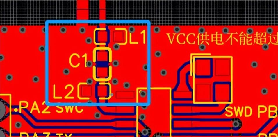
2. For a two-layer board, it is recommended that the line width of the matching circuit be 0.5mm, and the copper spacing for the matching circuit be 0.152mm (6mil), following a 50-ohm routing.3. The matching circuit should be surrounded by GND vias to ensure the effectiveness of the matching circuit.4. The crystal oscillator layout should be as close to the chip as possible for accurate clocking, and the traces should be as wide as possible.
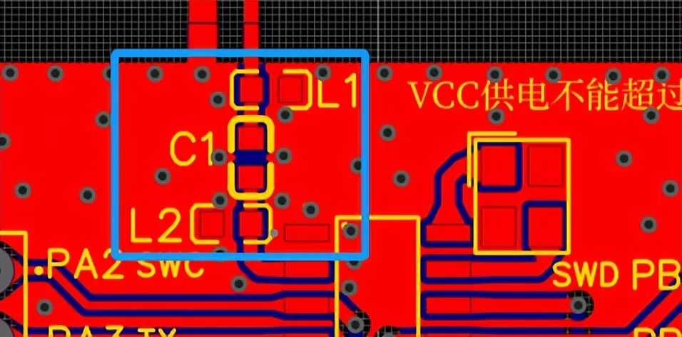
5. When using an onboard antenna, a row of GND vias must be placed in the copper separation area.6. The matching circuit area must not have traces or other components; keep this area clear, especially from high voltage and high current lines, as they have a significant impact.7. For circuits and components with high current and high voltage, it is recommended to use separate copper GND, isolating it from the RF circuit, and connect them with a 0-ohm resistor.8. For products requiring a communication distance of over 200 meters, it is recommended to use a two-stage PA, which means two amplification circuits to increase transmission power; the required 12V voltage can be achieved using a boost chip.2. Design Recommendations for 433.92HZ Application Circuits
1. XL4456 FCC/ETSI Certified Application Circuit
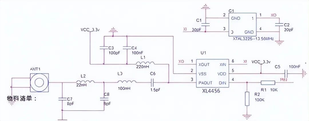
Grounding: Use as many vias as possible on the metal base plate to reduce parasitic inductance.
(1) Power bypass: To ensure the components work well, it is recommended to use a 0.1μF capacitor for filtering at the power lead, with the capacitor placed close to the component.
(2) When using a button battery for transmission, do not place the battery and PCB together; reduce the contact area between the battery and PCB.
(3) For transmission, add a PA circuit and a transistor amplification circuit to increase transmission power.
2. XL520 Standard Receiving Circuit
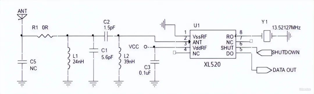
Note: In the above image, the antenna matching network components L1, C1, C2, and L2 are parameter values used during testing with an RF signal source. R1 and C5 are reserved for the matching network, facilitating RF matching adjustments based on the actual board. In practical use, a capacitor or inductor may be soldered at R1, and one of the components C5, L1, or C1 should be soldered. C2 and L2 should remain unchanged. Thus, in practical applications, the number of components in the antenna matching network remains four. Specific soldering parameters should be determined based on the actual board debugging situation.
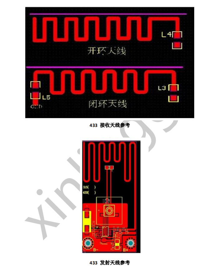
3. 433MHZ Antenna Design
1. The antenna must strictly follow the reference design.
2. The surrounding enclosure cannot be a sealed metal case; the area near the antenna must be made of plastic material (and should not have coatings containing metallic particles).
3. The antenna should be kept away from the output stage (especially when the output stage is class D) and the magnetic steel of the speaker (if there is a speaker nearby, use a magnetically shielded speaker if possible).
4. The distance between the antenna and other conductors must be greater than 15mm, and it should be as close to the enclosure as possible.
5. The RF routing must have a complete reference ground and follow 50-ohm routing. Consider using RF cables and dedicated PCBs for antenna placement.
6. The routing of the antenna and audio preamp as well as the MIC should be kept as far apart as possible to prevent RF interference with audio. The differential routing of audio should be as parallel and equal in length as possible, and no ground line should be placed between the two lines.
7. RF routing should not pass under the module, as the bottom of the module is generally a GND layer. If the RF line runs on the main top layer and then passes under the module, it will be very close to the GND of the module’s bottom, which greatly affects the signal.
8. Additionally, RF routing vias also affect the signal and should be avoided as much as possible.
9. The antenna area must not have components or other routing.
10. For S-shaped antenna routing, the spacing between lines should be three times the line width (for example, if the line width is W=0.8mm, the spacing should be 2.4mm).