In 2017, Google updated their TPU series. Google referred to this generation of TPU as a “domain-specific supercomputer for training neural networks.” It is evident that compared to TPU v1, which focused on inference scenarios, TPU v2 shifted its design focus towards training-related scenarios. Looking back at history, around 2017, groundbreaking work in deep learning emerged like mushrooms after rain. It was that year that Google published the revolutionary paper “Attention Is All You Need” at NIPS (now NeurIPS), which completely transformed the world of NLP and set the trend for the next decade. One can imagine that this paper was not only the result of the tireless efforts of the Google Brain research team but also the culmination of years of work in the field of deep learning. Now, let’s talk about TPU v2, the supercomputer behind Attention.。
Changes in TPU v2 Business Scenarios
Inference is the process of obtaining model outputs through a single forward pass based on the trained model structure and parameters. Compared to training, inference does not involve gradient and loss optimization; therefore, alongside the robustness of the neural network model, the model’s demand for data precision is relatively low. In contrast, the training process is significantly more complex than inference. Generally, the training process involves designing appropriate AI model structures, loss functions, and optimization algorithms, repeatedly performing forward calculations on the dataset in mini-batches, calculating losses, and backpropagating gradients to update the model, minimizing the loss function to achieve model convergence. The most critical step in the training process is the calculation of gradients and backpropagation, during which common tools in engineering, such as optimizers and learning rate schedulers, also need to be calculated, making the precision of data calculations extremely important. If an issue arises at any computation node, it could lead to problems such as gradient explosion or gradient vanishing, preventing the model from converging.
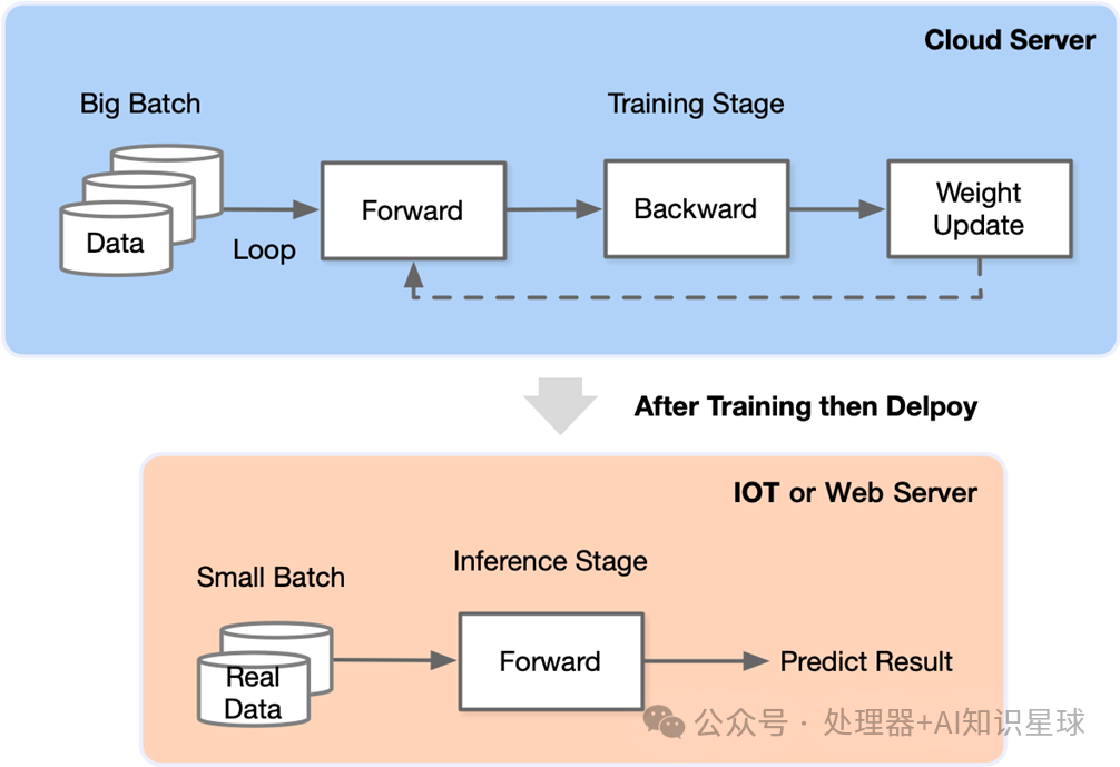
The following diagram illustrates a simple representation of model training (top) and inference (bottom). We can see that in the training scenario, the model and data need to continuously cycle through the process of “forward propagation
arr backward propagation
arr weight update” until the weights converge. The prepared model is then deployed in a production environment, where each time new data arrives, it only needs to perform a forward pass through the deployed model to obtain the model output and put it into production.
Challenges in Training Scenarios
So, what are the specific challenges in training scenarios?
-
More challenging data parallelism: In the inference phase, each inference task is independent, allowing DSA chip clusters to scale horizontally. However, in training scenarios, a model needs to iterate millions of times, and all parameters of the model must be adjusted in each iteration, requiring coordination for parallel computation across clusters.
-
Higher computational complexity: Backpropagation requires calculating the partial derivatives of every weight parameter and input at each stage of the model, including higher precision activation values and matrix multiplication calculations of transposed weight matrices \(W^TW^TW\).
-
Greater memory requirements: The data for weight updates comes from temporary variables during forward and backward propagation. Temporary variables need to be retained at each layer of the model, increasing the load on existing resources. In large models, temporary variables, including activation values and optimizer values at each layer, can inflate the model size to 8-9 times its original size.
-
Higher programmability: Rapid changes in training algorithms and models may render designs obsolete quickly, necessitating training chips to have higher programmability to adapt to the ever-evolving model architectures.
-
High precision data formats: Integer INT8 can be used for inference, but during training, it is essential to capture gradient information adequately, typically requiring mixed precision computations such as FP16, BF16, and FP32 to ensure model convergence.
TPU v2 vs. TPU v1
In the face of numerous challenges, Google’s engineers made some subtle improvements based on the first generation TPU to adapt to training scenarios. What specific changes were made?
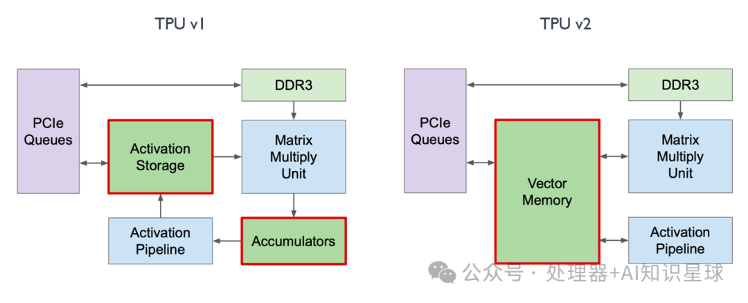
Change 1: Vector Memory
In TPU v1, we can see that it has two storage areas:
-
Accumulator responsible for storing matrix multiplication results
-
Activation Storage responsible for storing activation function outputs
In inference scenarios, dedicated storage modules are very helpful for computation and storage as they are more domain-specific. However, during training, to enhance programmability, as shown in the diagram below, TPU v2 swapped the positions of the Accumulators and Activation Pipeline, merging them into Vector Memory, making it more akin to L1 Cache in traditional architectures, thereby enhancing programmability.
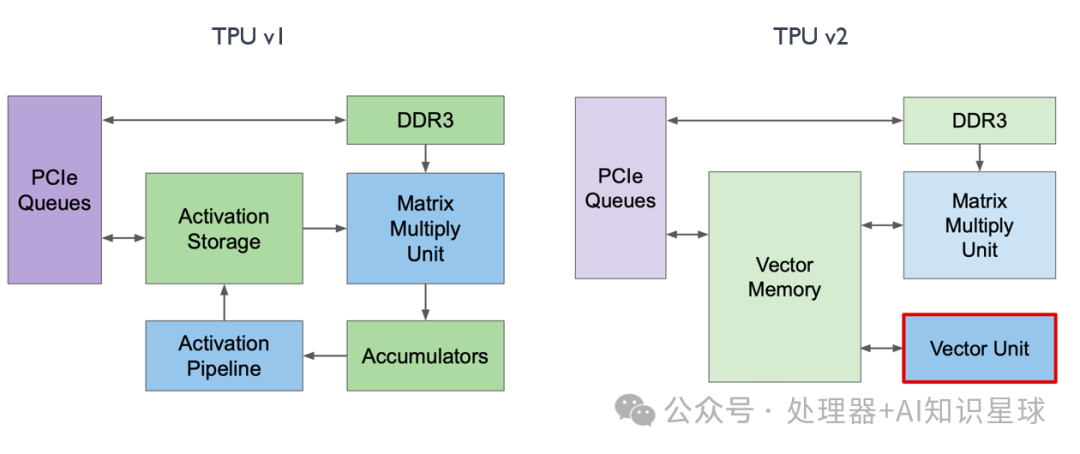
Change 2: Vector Unit
In TPU v1, the Activation Pipeline was specifically designed for activation function scenarios, i.e., after convolution, there is a Batch Normalization followed by a special activation function ALU computation. However, this specialized ALU computation could not meet the needs of training scenarios. Therefore, as shown in the diagram below, the former Activation Pipeline in TPU v2 has transformed into a Vector Unit, specifically designed to handle a series of vector activation functions.
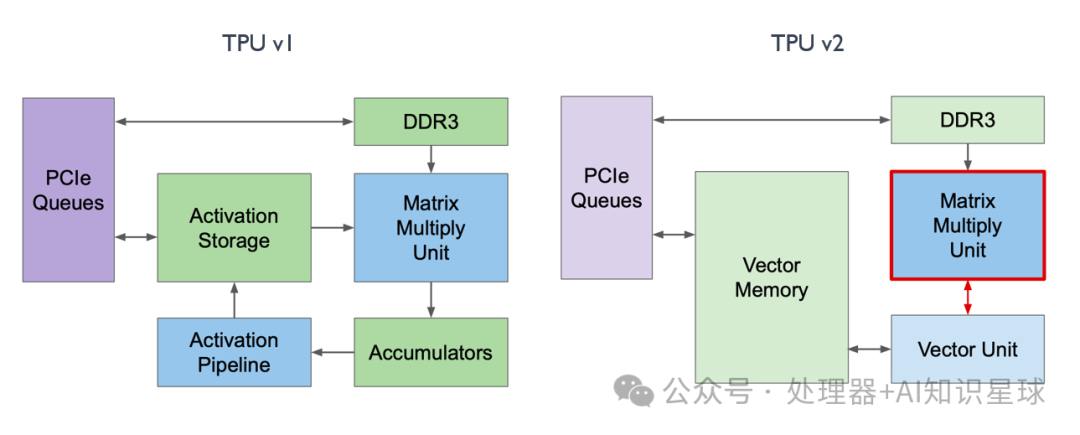
Change 3: MXU
In TPU v1, the MXU was connected to Vector Memory, while in TPU v2, Google connected the MXU to the Vector Unit, with all data outputs and computations being distributed by the Vector Unit. This way, all matrix-related computations of the MXU became co-processors of the Vector Unit, making it more user-friendly for compilers and programmers.
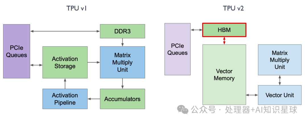
Change 4: DDR3
In TPU v1, DDR3 memory was used to directly load some weights needed for computation in inference scenarios. However, during training, many intermediate variables and weights are generated, and the write-back speed of DDR3 cannot meet the demand. Therefore, in the training process of TPU v2, as shown in the diagram below, we placed DDR3 alongside Vector Memory and replaced DDR3 with HBM, resulting in a 20-fold increase in read and write speeds.
TPU Computing Core
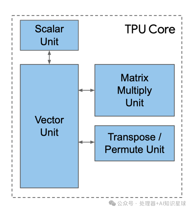
Scalar Unit
The above image is a simple illustration of the TPU core. We can see that the scalar unit is the starting point for processing computations. It fetches complete VLIW (Very Long Instruction Word) from the instruction memory, executes scalar operations, and passes the instructions to the vector and matrix units for further processing. VLIW consists of two scalar slots, four vector slots (two for vector load/store), two matrix slots (one for push and one for pop), one miscellaneous slot (a simple example is a delay instruction), and six immediates.
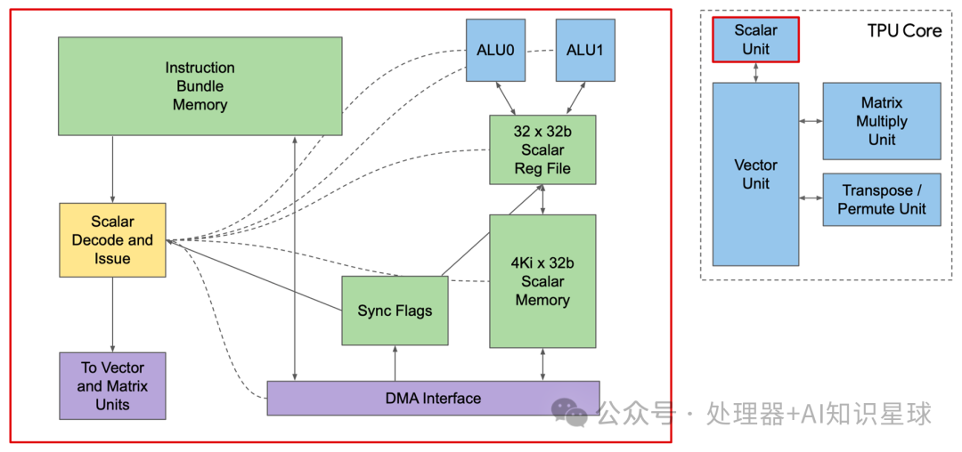
Now, let’s look at where the instructions are obtained. The Core Sequencer no longer fetches instructions from the CPU but retrieves VLIW instructions from Instruction Mem, using 4K 32-bit scalar memory to perform scalar operations, with 32 32-bit scalar registers, while sending vector instructions to the VPU. The 322-bit wide VLIM can send 8 operations, two scalars, two vector ALUs, vector load, vector store, and a pair of queued data from matrix multiplication.
Vector Unit
As shown in the right side of the diagram below, the Vector Unit is connected to the Scalar Unit. The left image shows one of the Vector Lanes, and the entire Vector Unit contains 128 such vector lanes. Each lane has an additional 8-way execution dimension, known as sub-lanes. Each sub-lane is equipped with a dual-issue 32-bit ALU and connected to a 32-depth register file. This design allows the vector computing unit to operate on 8 groups of 128-width vectors simultaneously in each clock cycle, and the sub-lane design enhances the ratio of vector to matrix computations, making it particularly suitable for batch normalization operations.
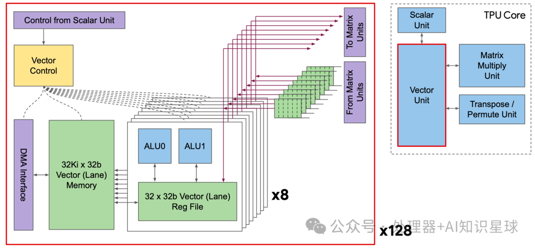
Matrix Multiplication Unit (MXU)
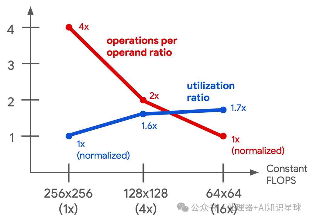
MXU has always been the core of TPU. TPU v2 opted for a 128 \times 128 MXU instead of the 256 \times 256 MXU used in TPU v1, primarily due to considerations of utilization and area efficiency. In the diagram below, Google’s simulator indicates that the utilization of four 128 \times 128 MXUs in convolution models ranges from 37% to 48%, significantly higher than that of a single 256 \times 256 MXU (22% to 30%), while occupying the same chip area. This is because some convolution calculations are inherently smaller than 256 \times 256, leading to idle portions of the MXU. This means that using multiple smaller MXUs can achieve higher computational efficiency within the same area. Although sixteen 64 \times 64 MXUs have slightly higher utilization (38% to 52%), they require more area because the smaller MXU area is limited by I/O and control lines rather than multipliers. Therefore, the 256 \times 256 MXU achieves a better balance between bandwidth, area, and utilization, making it the optimal choice for TPU v2.
In addition to becoming smaller, this generation of MXU has the following main features:
-
Numerical and precision: Multiplication operations use the bfloat16 format, which has the same exponent range as float32 but fewer mantissa bits. Accumulation uses 32-bit floating-point numbers.
-
Energy efficiency: Compared to IEEE 16-bit floating-point numbers, bfloat16 offers approximately 1.5 times the energy efficiency advantage.
-
Adoption and ease of use: Compared to fp16, bfloat16 is easier to use for deep learning as it does not require loss scaling. Due to this ease of use, along with energy efficiency and area efficiency, bfloat16 has been widely adopted in the industry and is one of the most important building blocks in deep learning.
Transpose/Reduction/Permutation Core (TRP Unit)
This core is used for special computation operations on 128 \times 128 matrices (such as Transpose, Reduction, Permute), allowing matrix data to be rearranged, enhancing programming ease. These steps are frequently encountered in matrix-related scenarios during training, especially in backpropagation, which is why TPU v2 has been specially optimized for this part.
Chip Interconnection Methods
When building modern supercomputers, the interconnection between chips becomes crucial. TPUv1 is a single-chip system used as a co-processor for inference. Training Google’s production models on a single chip would take months. However, TPU v2 is different. In the diagram below, we can see that Google designed an Interconnect module on the board for high-bandwidth scaling, enhancing the interconnection capabilities between TPU v2 chips, and based on this, built the TPU v2 Supercomputer (“Pod”).
This Interconnect module specifically refers to the Interconnect Router in the lower right corner of the diagram below.
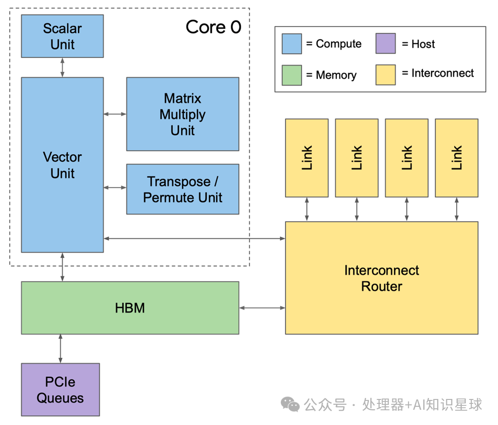
This module enables 2D toroidal connections, forming a Pod supercomputer. Each chip has four custom inter-chip interconnect (ICI) links, each running in TPU v2, with a bandwidth of 496 Gbit/s in each direction. ICI allows chips to connect directly, enabling the construction of a supercomputer using only a small portion of each chip. Direct connections simplify rack-level deployment, but in multi-rack systems, racks must be adjacent.
TPUv2 Pod uses a 16×16 two-dimensional ring network (256 chips), with a bidirectional bandwidth of 32 links x 496 Gbit/s = 15.9 Terabits/s.
In contrast, a single Infiniband switch (for CPU clusters) connecting 64 hosts (assuming each host has four DSA chips) has 64 ports, using “only” 100 Gbit/s links, with a maximum bidirectional bandwidth of 6.4 Terabits/s. TPUv2 Pod provides 2.5 times the bidirectional bandwidth of traditional cluster switches while eliminating the costs of Infiniband network cards, Infiniband switches, and latency costs associated with communication through CPU hosts, significantly enhancing overall computational efficiency.
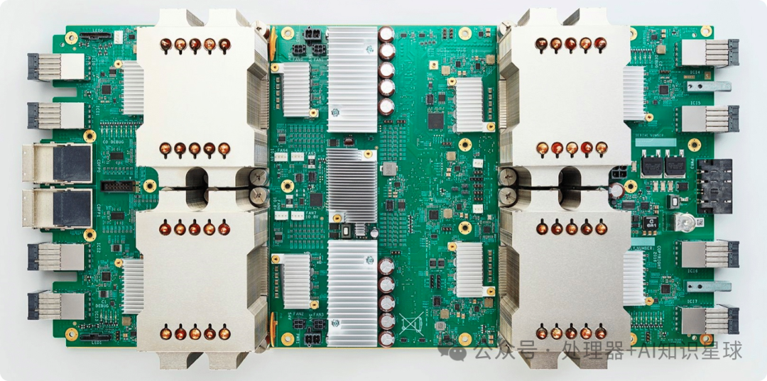
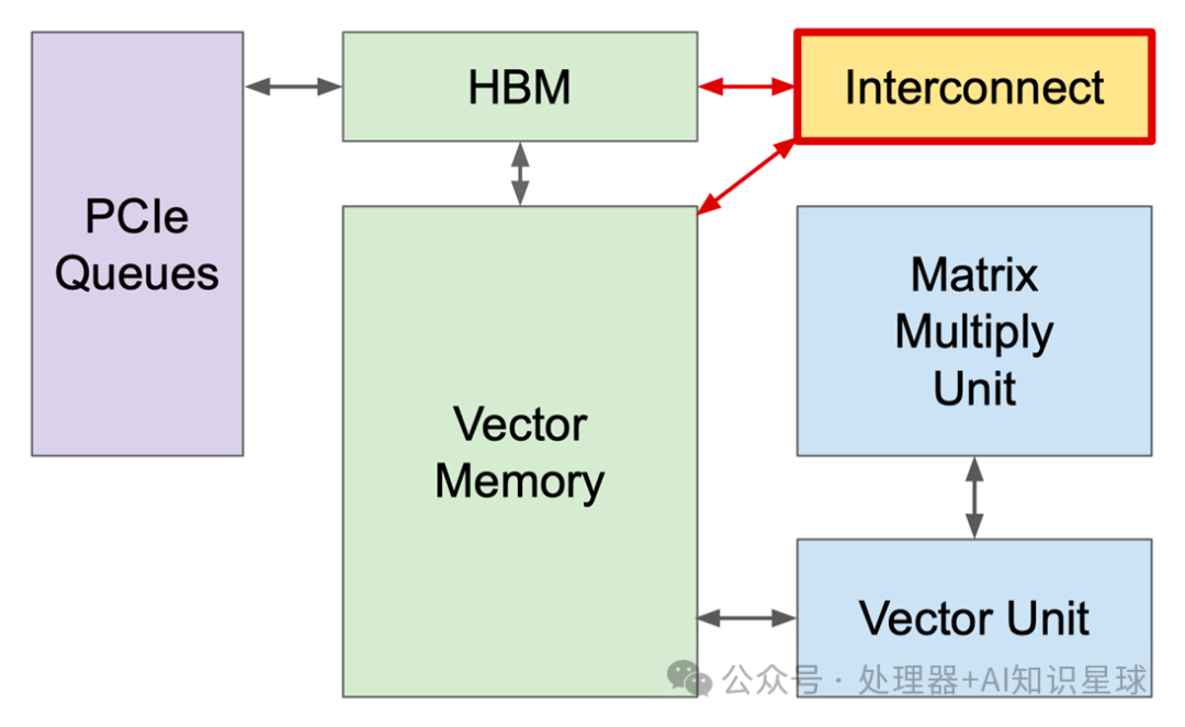
The above content revolves around a TPU module. In fact, the first image in this article shows that the TPU v2 module consists of multiple chips, and the interaction between these chips is facilitated by the interconnect module discussed above. As shown in the diagram below, an interconnect module is responsible for interacting with multiple TPU chips and storage to maximize computational efficiency.
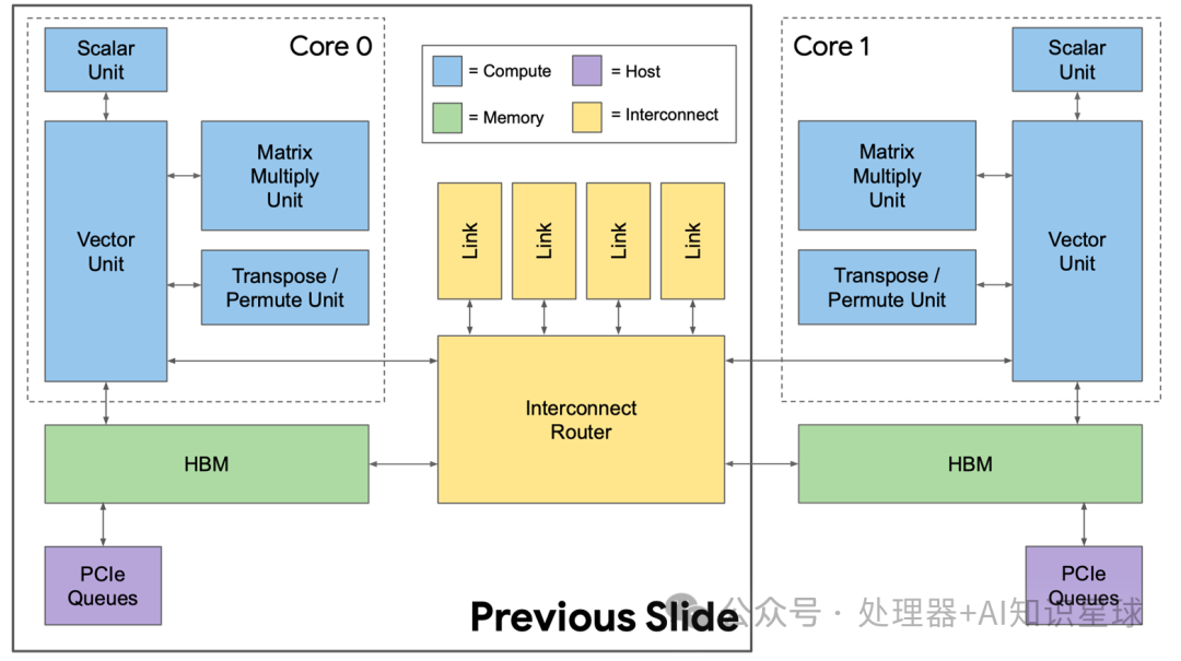
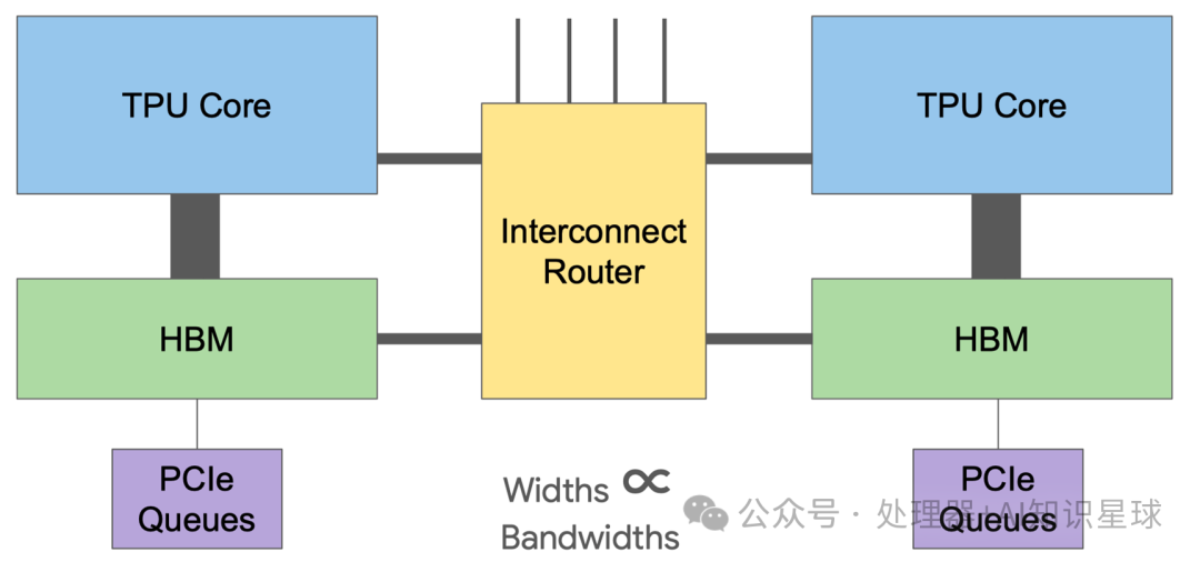
The overall architecture diagram is shown below, where the thickness of the lines represents the bandwidth. The TPU core and HBM storage have the largest bandwidth, followed by the TPU core, HBM, and Interconnect Router bandwidth.
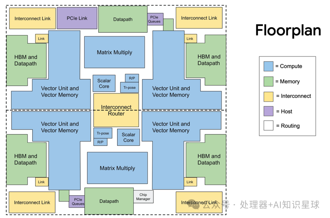
Chip Architecture Layout
The following is the layout diagram of TPU v2. We can see that most areas are occupied by blue computing cores, while the memory system and interconnect occupy the remaining significant portion. Two TPU cores are positioned one above the other, with the interconnect router located in the central hole providing interconnection between the cores, and the two MXUs located at the top center and bottom center providing the core pulsing array computing capability, while the remaining space is filled with wiring.
Summary and Thoughts
-
Google TPU v2 is a domain-specific supercomputer designed for training neural networks. Unlike TPU v1, which focuses on inference, TPU v2 is specially optimized for training scenarios.
-
TPU v2 improves programmability, computational complexity handling, and memory requirements during the training process through enhancements in key components such as Vector Memory, Vector Unit, MXU, and DDR3.
-
The matrix multiplication unit (MXU) used in TPU v2 employs the BF16 format for multiplication operations, providing high energy efficiency and user-friendly deep learning performance.
-
TPU v2 achieves large-scale Pod supercomputers through efficient inter-chip interconnection technologies, such as 2D toroidal connections and high-bandwidth Interconnect Routers, significantly enhancing overall computational efficiency.
Content organized from Bilibili expert ZOMI, welcome to follow!
Related Reading:
History of Google TPU
Google TPU v1 – Pulsing Array