Bluetooth has always been a standard feature for smart devices, whether it be smartphones, laptops, or tablets. With the development of mobile internet, a large number of smart wearable devices have emerged, and the development of these applications requires not only mobile software support but also support from wireless sensing technology. Bluetooth remains the preferred communication method for wireless connections.
Bluetooth technology is a crucial component in this ecosystem. It demands sensitivity in communication, miniaturization, low power consumption, and importantly, low cost.
The emergence of Bluetooth 4.0 addresses these issues, incorporating Bluetooth Smart (low power) functionality with the following features:
1) Low energy consumption
2) Low cost
3) Standard button batteries can power devices for several years
4) Multi-vendor interoperability
5) Enhanced range
In hardware design, antenna design is quite critical. A common low-cost design method is the PCB onboard antenna design. But how should the PCB onboard antenna be designed in practice to achieve good transmission and reception performance? Below are four Bluetooth antenna design methods for reference:
Bluetooth Antenna Design – Inverted-F Antenna:
The antenna body of the inverted-F antenna can be either linear or planar. When using a dielectric material with a higher dielectric constant, the size of the Bluetooth antenna can be reduced. As a type of onboard antenna, the inverted-F antenna design is low-cost but increases in volume, making it one of the most common designs in practice. The antenna is generally placed on the top layer of the PCB, and the ground plane is laid on the top layer and located near the antenna, but no ground should be placed around the antenna, which should be a clear area. As shown in the figure below:
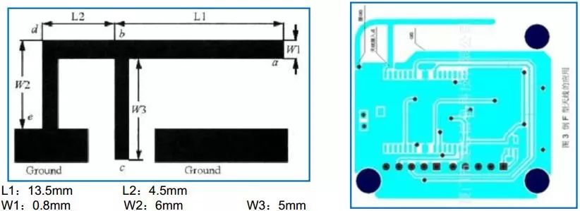
Figure 1: Inverted-F Antenna Design Schematic
Bluetooth Antenna Design – Meandered Antenna:
The length of the meandered antenna is relatively difficult to determine. It is generally slightly longer than a quarter wavelength, and its length is determined by its geometric topology and the ground plane. The meandered antenna is generally PCB packaged, i.e., an onboard antenna. Similar to the inverted-F, the antenna is generally placed on the top layer of the PCB, and the ground plane is laid on the top layer and located near the antenna, but no ground should be placed around the antenna, which should be a clear area. As shown in Figures 2 and 3:
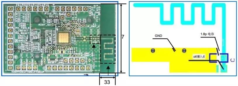
Figure 2: Meandered Antenna Design Schematic 1
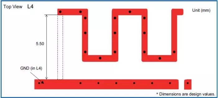
Figure 3: Meandered Antenna Design Schematic 2
Note: Antenna length calculation formula:
Antenna length (meters) = (300/f) * 0.25 * 0.96
Where f represents frequency (MHz), and 0.96 is the wavelength shortening rate
The length of a Bluetooth antenna is approximately 300/2.4G * 0.25 * 0.96, which is about 31mm.
Bluetooth Antenna Design – Ceramic Antenna:
Ceramic antennas are another type of miniaturized antenna suitable for Bluetooth devices. Ceramic antennas can be categorized into block ceramic antennas and multilayer ceramic antennas. Due to ceramics having a higher dielectric constant than PCB circuit boards, using ceramic antennas can effectively reduce antenna size. In terms of dielectric loss, ceramic materials also have lower dielectric loss than PCB circuit boards, making them very suitable for low-power Bluetooth modules. In PCB design, it is sufficient to have a clear area around the antenna and it is especially important not to place copper around it. As shown in the figure below:
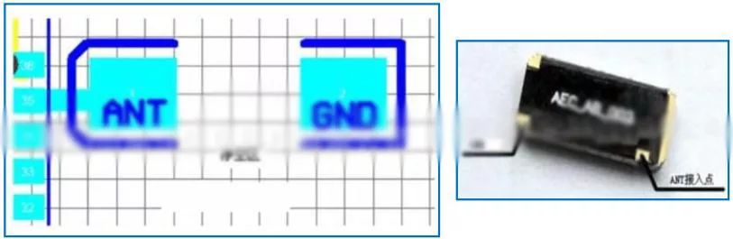
Figure 4: Ceramic Antenna Design Schematic
Bluetooth Antenna Design – 2.4G Rod Antenna:
The 2.4G rod Bluetooth antenna is larger but has a stronger transmission distance than other antennas. In PCB design, the area around the antenna must also be clear, just like the previous three antenna designs. As shown in the figure below:
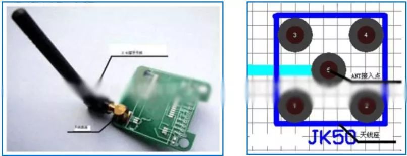
Figure 5: 2.4G Rod Antenna Design Schematic
Other Related Considerations for Bluetooth Antenna Design:
1) The antenna signal (frequencies above 400MHz) is susceptible to attenuation, so the distance between the antenna and nearby ground should be at least three times the line width.
2) For microstrip and stripline, the characteristic impedance is related to the thickness of the board layers, line width, vias, and the dielectric constant of the board material.
3) Vias can introduce parasitic inductance, which can cause significant attenuation for high-frequency signals, so try to avoid vias when routing RF lines.

Source: Shiqiang; RFsister Editing整理
Reprint Statement: This article aims to provide industry information reading for the RF technology circle. If there are inaccuracies or infringement issues, please contact us for processing! Respect knowledge, respect originality!
Submission email: [email protected]
Reply with the keyword【Public Course】 to obtain the following activity materials:
“MIMO Technology Principles and Measurement”, “MIMO OTA Test Cases and Case Analysis”
“Mobile Terminal (Phone) MIMO OTA Testing Technology”
“Global Wireless Product Certification Knowledge” and “Analysis of Overseas Market Access Rules and Processes”
NB-IoT Technical Materials |“High-Speed PCB Design Techniques Comprehensive Analysis” | “RFID Development and Application”
“Full Process Analysis of Mobile Phone RF Development” | “CST Antenna Simulation and Design”
“Full Process of Onboard Antenna Design and Development” | “Terminal Small Antenna Design”
Huawei P9, iPhone X Teardown Analysis Report (including high-definition images, test data)
Spectrum, Oscilloscope, and Network Distribution Demonstration Materials