1. Introduction
In previous articles, we introduced some basic principles of SDRAM. This article will introduce the SDRAM controller under the FMC of STM32F429.
2. Introduction to the SDRAM Controller of STM32F429
According to the general module driver initialization process, it mainly involves the clock path: clock source to clock division configuration, enabling clocks for each module, etc. Then there is the corresponding pin configuration: function multiplexing, pin speed, etc. Finally, there is the configuration of the module itself. Therefore, the following introduction will follow the above thought process.
2.1 Clock
The clock comes from the HCLK divided by 2 or 3 (as described in the manual P1666), configured through the register FMC_SDCR1 for SDCLK.

And the source of HCLK can be configured according to the clock tree, with a maximum of 180MHz
There is an 8MHz HSE external crystal on the development board.
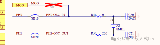
Thus, the HSE is processed through the PLL to obtain a 180MHz HCLK, and finally, the clock for SDRAM is either 90MHz or 60MHz.
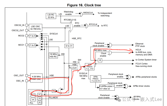
When configuring the clock to 180MHz, there are some points to note, which will be detailed in the later articles regarding the driver implementation.
Additionally, the clock for the FMC itself needs to be enabled, configuring the RCC_AHB3ENR for FMCEN
Of course, the corresponding port clock for the pins Px must also be enabled.
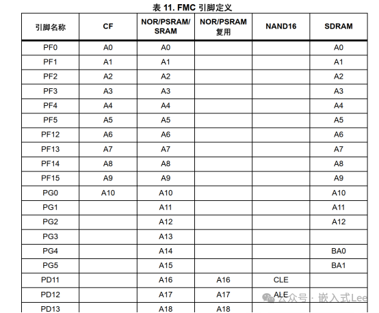
2.2 Signals/Pins
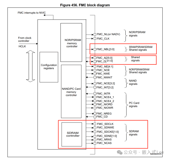
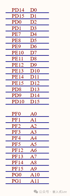
Address lines A, up to 13 lines
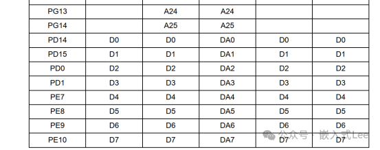
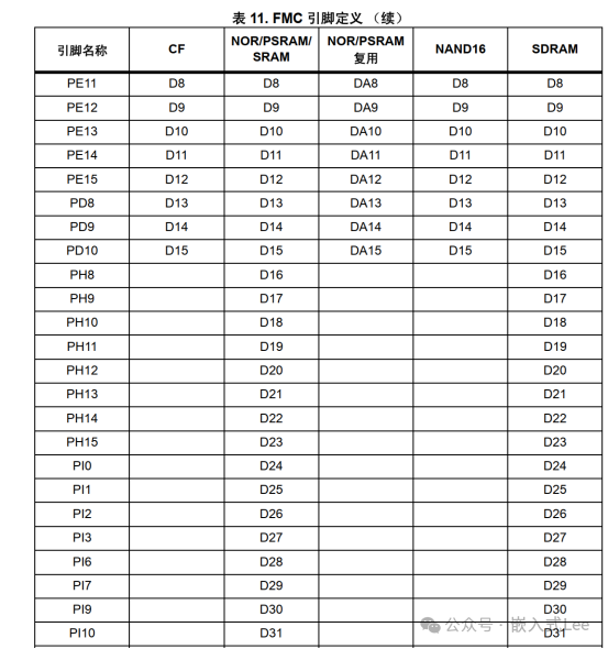
Data lines D, up to 32 lines
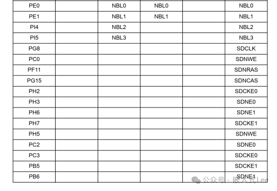
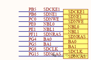
And control lines (10 signals, with SDCKE and SDNE having two, corresponding to two chip selects for two BANK address spaces, while other signals are multiplexed for multiple chips)
As shown in the figure, the signals BA0 and BA1 are not reflected.
The meanings of each signal are as follows:
Among them, SDCKE and SDNE are the clock enable and chip select signals, respectively, with two available, allowing for two chip selects corresponding to two BANK address spaces, namely SDRAM BANK1 and SDRAM BANK2. Note that the BANK here refers to the internal address space of the STM32F429, not the storage bank within the SDRAM chip itself. Therefore, it can be expanded through different chip selects, which is a series connection method, where all signals except SDCKE and SDNE are multiplexed, actually corresponding to different address spaces, with two independent BANK spaces controlled independently within the controller, also corresponding to different control and timing registers.
NBL is the byte MASK, for 8 bit address bus only NBL0 is needed, for 16 bits, both NBL0 and NBL1 are needed, and for 32 bits, all 4 are needed. Here, if multiple SDRAM chips are used in parallel, the expanded bus width is considered as a single chip with a wider bus, where only the data lines are expanded, and all other signals are shared.
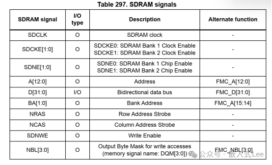
All signals change on the falling edge of FMC_SDCLK because data is transmitted on the rising edge.
The corresponding FMC pins can be seen in the data sheet, with the SDRAM pins all having AF12 function multiplexing.
Some signals such as SDNWE, SDCKE0/1, and SDNE0/1 can be mapped to different pins.
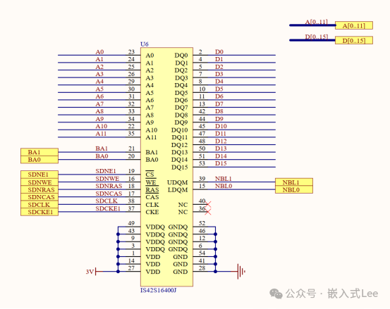
The schematic of the development board is as follows, with SDCK1 and SDNE1 corresponding to the SDRAM BANK2 address space.
It connects to an 8MB SDRAM with a 16-bit bus width. 4 banks, 12 row lines, and 8 column lines, meaning the row size (PAGE size) is 2^8 x 16 bits.
4 banks x 2^12 x 2^8 x 16 bits = 8MB.
Here is a brief introduction to each signal:
A: Address lines, used to provide row and column addresses(row and column addresses are provided in time), 12 bits for row addresses, so a maximum of 12 lines are needed.
D: Data lines, here it is 16 bits wide.
NBL0/1 : Since the data width is 16 bits, which is 2 bytes, two MASK signals are needed to mask off any unnecessary bytes.
BA0/1: Internal 4 banks of the SDRAM chip, used to address the internal 4 banks of the SDRAM chip.
SDNE1: Chip select signal, here using SDRAM BANK1.
SDNWE: Read/write signal
SDNRAS: Row address signal, indicating that the current A is transmitting a row address
SDNCAS: Column address signal, indicating that the current A is transmitting a column address
SDCLK: Clock
SDCKE1: Clock enable, here using SDRAM BANK2
2.3 Basic Features
The SDRAM controller belongs to FMC. It supports SDRAM and Mobile LPSDR SDRAM.
-
Two SDRAM BANKs, configured independently. That is, SDRAM BANK1/BANK2 corresponds to FMC BANK5 and BANK6.
-
Supports 8/16/32 bit buses. Byte masking is done through NBL signals, for SDRAMs with a bus width less than 32 bits, the controller automatically stitches them together when accessing memory, so the software is unaware of this, allowing for arbitrary 8/16/32 bit memory access, and the controller will automatically map it to the actual read/write in the SDRAM (which may involve fetching from FIFO or actual multiple reads/writes).
-
13 bit row address, 11 bit column address, 4 internal banks
For bus widths of 8/16/32, the maximum capacities are as follows:
4x16Mx32bit(256 MB), 4x16Mx16bit (128 MB), 4x16Mx8bit (64 MB)
Where 4 indicates 4 banks
Where 16M is calculated as follows:
16M=2^13 x 2^11=2^24=16M
The size corresponding to a row address corresponds to the PAGE size, which is 2^ column bits = 2^11 x bus width = 2K*width.
Thus, for 8 bit buses, the PAGE is 2KB, for 16 bits it is 4KB, and for 32 bits it is 8KB.
-
Supports word, half-word, and byte access
-
The clock is HCLK/2 or HCLK/3
-
Automatic row and column address boundary management
-
Multi-bank ping-pong operations
-
Programmable timing parameters
-
Auto-Refresh, with configurable refresh rate, the controller automatically sends refresh commands at specified intervals.
-
Self-refresh mode, with no clock, the SDRAM refreshes itself internally.
-
Power-down mode, the SDRAM controller automatically exits power-down, sends auto-refresh commands, and then re-enters power-down.
-
SDRAM initialization sequence is executed by software
-
CAS can be configured to 1, 2, or 3
-
Cacheable Read FIFO depth of 6 lines x 32-bit (6 x 14-bit address tag)
2.4 REMAP
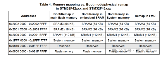
FMC SDRAM bank 1 can be REMAPped to address 0.
Accessing through the ICode bus improves performance, and it can also be accessed through the original address space.
Configured through the register SYSCFG_MEMRMP with the MEM_MODE bits, which are used to configure the type of memory accessible at address 0x00000000, allowing for physical remapping through software.
After reset, these bits take the value selected by the BOOT pins (FMC cannot be selected by BOOT, it can only be configured by software, so it cannot boot from FMC).
When booting from the main flash, the BOOT pins are set to 10[ (BOOT1, BOOT0) = (1,0)], the value of this register is 0x00.
Software modifies these bits to override the configuration of the BOOT pins.
00: Main Flash memory mapped to 0x0000 0000
01: System Flash memory mapped to 0x0000 0000
10: FSMC Bank1 (NOR/PSRAM 1 and 2) mapped to 0x0000 0000
11: Embedded SRAM (SRAM1) /FMC SDRAM bank 1 mapped to 0x0000 0000
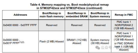
2.5 Address SWAP of SDRAM BANK
The register SYSCFG_MEMRMP with the SWP_FMC configures whether the address space of SDRAM banks and NAND Bank 2/PCCARD, i.e., FMC Bank 3/4, is swapped, which also affects the swapping of FMC Bank 1/2, but here we only care about SDRAM.
00: No SWAP
01: SWAP
10: Reserved
11: Reserved
If not swapped, the addresses of SDRAM bank1/2 are 0xC0000000 and 0xD0000000,
If swapped, the addresses are 0x80000000 and 0x90000000.
Here, our address is 0x90000000, indicating that swapping is needed and we are using SDRAM bank2
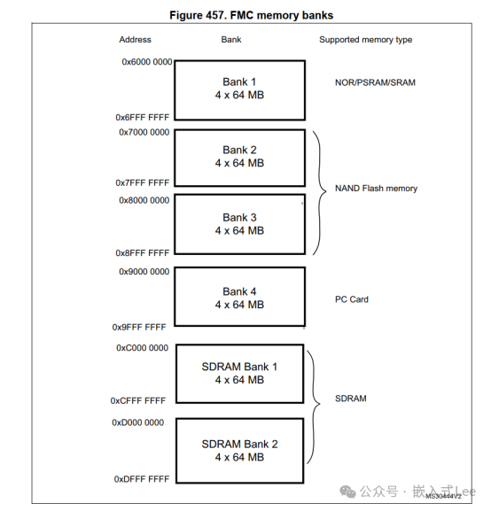
SDRAM corresponds to FMC BANK5 and BANK6.

2.6 Read FIFO
Read FIFO is enabled only when Burst is used.
Cacheable Read FIFO with 6 x32-bit depth (6 x14-bit address tag) for SDRAM controller.

2.7 Maximum Space
2 BANKs, each BANK has a maximum space of 256MB, and the maximum AHB address is 28 bits.
Different base addresses correspond to different BANKs.
2.8 Write Protection
Writing to the SDCR register configured with WP for SDRAM will generate AHB errors.
Accessing beyond the SDRAM address range will also generate AHB errors.

2.9 Address Space
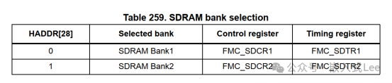
SDRAM has two BANKs, and HADDR[28] determines which SDRAM BANK is accessed.
Address 0x80000000/0xC0000000 bit28=0 corresponds to BANK1
Address 0x90000000/0xD0000000 bit28=1 corresponds to BANK2
Each BANK has a maximum of 256MB.
The maximum row address is 13-bit, configurable to 11, 12, 13
The maximum column address is 11-bit, configurable to 8, 9, 10, 11
Supports a maximum of 4 internal BANKs for DRAM, and can be configured to 2 or 4.
Bus width supports 8, 16, 32.
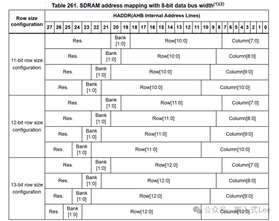
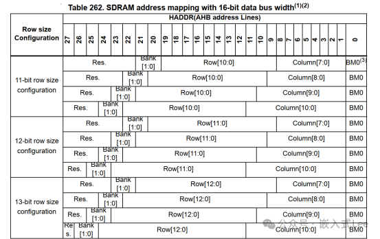
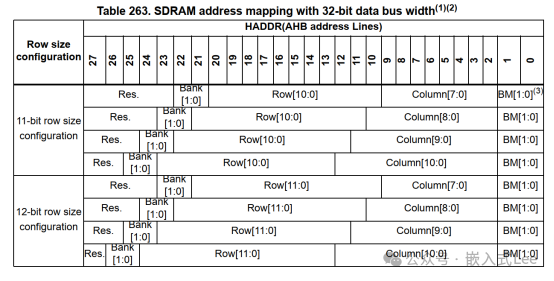
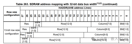
The internal HADDR address corresponds to the bank-row-column address of SDRAM as follows:
HADDR is in bytes, but the bank-row-column address corresponds to the bus width, so
When the bus width is 8bits, HADDR[0] corresponds to column[0]
When the bus width is 16bits, HADDR[1] corresponds to column[0]
When the bus width is 32bits, HADDR[2] corresponds to column[0]
Regardless of the bus width, FMC_A[0] is always connected to the SDRAM chip’s A[0], and the mapping of HADDR is done internally by the controller.
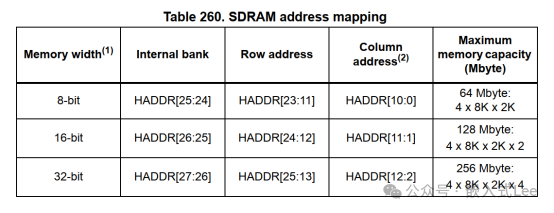
8-bit bus width: 12 configurations
16-bit bus width: 12 configurations, BM0 is used for byte mask, BM0 is an internal signal of the controller, not a signal on the pins, FMC_A0 connects to the SDRAM’s A0 without offset, this address offset is handled internally by the controller.
32-bit bus width: 12 configurations, BM[1:0] is used for byte mask
AutoPrecharge is not supported, FMC_A[10] must connect to A[10], during AutoPrecharge, A10 is always driven low.
3. Initialization
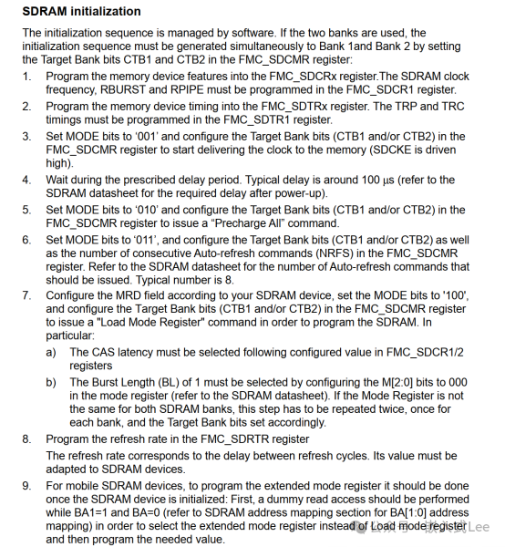
There are two sdram banks, and the CTB1, CTB2 of FMC_SDCMR determines whether to operate on sdram bank1 or sdram bank2.
1.The control registers of the two sdram banks are independent, and the configuration of FMC_SDCR1 or FMC_SDCR2
2.Configure timing parameters for the two banks separately using FMC_SDTR1 and FMC_SDTR2. TRP and TRC are configured by FMC_SDTR1
3.Set the MODE bits to “001”, configure CTB1 or CTB2 in the FMC_SDDMR register, and start sending clock to the memory (SDCKE is driven high).
4.Wait for the power-on delay according to the SDRAM manual.
5.Execute Precharge All, setting the MODE bits to “011”, and continuously send auto-refresh commands (NRFS) as needed, the number of which should refer to the SDRAM manual, generally 8.
6.Set the MODE bits to “100”, execute the load mode register command, and configure the mode register’s MRD, configuring CAS, and M[2:0] to configure BL=1
7.Configure the refresh rate using the FMC_SDRTR register.
8.For mobile SDRAM, the extended mode register also needs to be configured.
Note that for loading the mode register, self-refresh, the two BANKs share common parameters, determined by FMC_SDTR1 ‘s TMRD, TRAS, TXSR parameters.
For details, refer to the later driver implementation and check the register configuration process against the code.
4. Read and Write Operations
4.1 Write
Writing to memory, the controller automatically switches to single or Burst write for the SDRAM.
The SDRAM controller tracks the active row of each bank to enable continuous write access to different banks (multi-bank ping-pong access), so the software only needs to access any address, and the hardware will handle it automatically.
Before writing, the write protection bit WP of FMC_SDCRx must be cleared.
Write waveform
The hardware will automatically check the subsequent operation of a write operation
If the subsequent operation is still on the same row, or another active row, it can continue directly;
Otherwise, it will automatically precharge the current row, then activate a new row for the new write operation.
4.2 Read
Reading and writing have similar characteristics.
Additionally, reading has a Cacheable read FIFO (6 lines x 32 bits).
Used to store data pre-read during CAS delay and RPIPE delay.
The anticipated data Number of anticipated data = CAS latency + 1 + RPIPE delay / 2
Must set the RBURST bit in the FMC_SDCR1 register to predict the next read access, otherwise, if the RBURST bit is not set, the FIFO will not be used.
For example:
• CAS latency = 3, RPIPE delay = 0: 4 data (not committed) are stored in the FIFO.
• CAS latency = 3, RPIPE delay = 2: 5 data (not committed) are stored in the FIFO
The read FIFO has a feature where each line has a 14-bit address tag to identify its content:
11 bits are used for column address, 2 bits are used to select the internal bank and active row, and 1 bit is used to select the SDRAM device (supporting two SDRAM BANKs).
When the AHB master requests the content at address 0, if it is not available, the controller will send a command to read from SDRAM, it does not just read one WORD when you request one WORD, because it anticipates that you will need continuous reads and will read multiple data at once into the FIFO. As for how much to read at once, it is determined by the number of anticipated data.
When you next read the data at address 4, the controller has already read it into the FIFO, so you only need to read from the FIFO.
At this point, if it is a continuous operation and on the same row, there is no need to send a new row. The controller can continue to read subsequent column addresses, and there is no delay at this point, with one clock reading one column.
At this point, the AHB only needs to read from the FIFO, and the controller automatically reads data from SDRAM into the FIFO, allowing for a pipeline flow, achieving high efficiency.
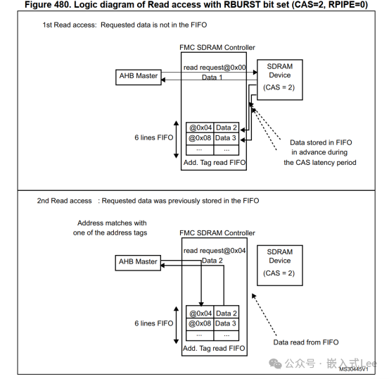
During write access or precharge commands, the read FIFO is refreshed and ready to fill with new data.
After the first read request, if the current access does not reach the row boundary, the SDRAM controller anticipates the next read access during the CAS wait time and RPIPE delay (if configured) by incrementing the memory address.
The following conditions must be met:
1.In the FMC_SDCR1 register, the RBURST control bit must be set to 1.
2.The address management depends on the next AHB request:
a)The next AHB request is sequential (AHB Burst).
In this case, the SDRAM controller increments the address.
b)The next AHB request is non-sequential.
If the new read request is to the same row or another active row, the new address is passed to memory, and the host will stall during the CAS delay period, waiting for new data from memory. If the new read request is not to an active row, the SDRAM controller generates a precharge command, activates a new row, and starts the read command.
RURST set to 0, the FIFO is not used.
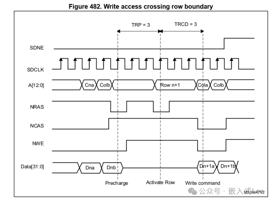
4.3 Row and Bank Boundary Management
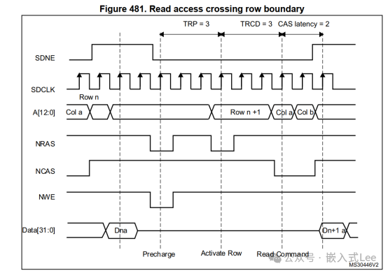
When read or write access crosses a row boundary, if the next read or write operation is sequential and the current access is at a row boundary, the SDRAM controller performs the following actions:
1.Precharge the active row, i.e., close the current row.
2.Activate a new row.
3.Execute read/write commands.
At row boundaries, regardless of the column size, the data bus width supports automatic activation of the next row.
If necessary, the SDRAM controller inserts additional clock cycles between commands, with relevant parameters configured in FMC_SDTRx.
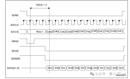
Match the TRP parameter between Precharge and Activate commands (only when the next access is to a different row within the same bank);
Match the TRCD parameter between Active and Read commands.
tRP is the interval between Precharge and sending the row address.
TRCD and CAS latency have been introduced earlier.
As shown in the write comparison, there is no CAS latency time, and the column address is written directly after the column address, while reading requires waiting for CAS delay. After all, reading has to wait for the SDRAM to have preparation time. Writing can directly place data into the SDRAM cache without waiting. However, reading from the cache does not necessarily have data, and it has to wait for the SDRAM’s logic to determine or even read data from the storage array into the cache, so it has to wait.
If the next access is sequential and the current access crosses the bank boundary, the SDRAM controller activates the first row in the next bank and starts a new read/write command. There are two possible scenarios:
-
If the current bank is not the last bank, the active row in the new bank must be precharged. At the bank boundary, all row/column and data bus width configurations support automatic activation of the next row.
-
For 13-bit row addresses, 11-bit column addresses, 4 internal banks, and 32-bit SDRAM memory, if the current bank is the last one, and the selected SDRAM device is connected to BANK1, the SDRAM controller continues to read from the second SDRAM device (assuming it has been initialized):
SDRAM controller activates the first row (after precharging the active row, if the first internal bank already has an active row, it activates the first row and starts a new read/write command.
If the first row is already activated, the SDRAM controller will only start the read/write command.
At the bank boundary, if the current bank is the last bank, only when addressing 13-bit rows, 11-bit columns, 4 internal banks, and 32-bit data bus SDRAM devices, will it support automatic activation of the next row. Otherwise, the SDRAM address range will be incorrect, resulting in AHB errors.
4.4 Refresh Cycle
Auto-refresh commands are used to refresh the contents of the SDRAM device, where the term Auto indicates that the SDRAM controller automatically sends refresh commands, not by software or the SDRAM itself.
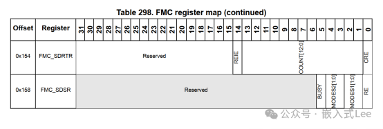
The SDRAM controller periodically issues auto-refresh commands. An internal counter loads the COUNT value in the register FMC_SDRR. This value defines the number of clock cycles between refresh cycles (refresh rate). When this counter reaches zero, an internal pulse is generated, and then a refresh command is sent, although it may not be able to send the refresh command at that time due to other operations in progress, requiring some judgment.
If memory access is in progress, the auto-refresh request will be delayed. However, if both memory access and auto-refresh requests are generated simultaneously, the auto-refresh request takes priority.
If a memory access occurs during an auto-refresh operation, the request is buffered and processed after the auto-refresh is completed.
If a new auto-refresh request occurs while the previous auto-refresh request has not been serviced, the RE (refresh error) bit is set in the status register. If interrupts are enabled (REIE=’1′), an interrupt will be generated.
If the SDRAM line is not in an idle state (with rows not closed), the SDRAM controller will generate a PALL (Precharge ALL) command before the auto-refresh.
If the auto-refresh command is generated by the FMC_SDCMR command mode register (mode bit = “011”), a PALL command must be issued first (mode bit = “010”). That is, in manual mode.
4.5 Low Power Mode
There are two low power modes:
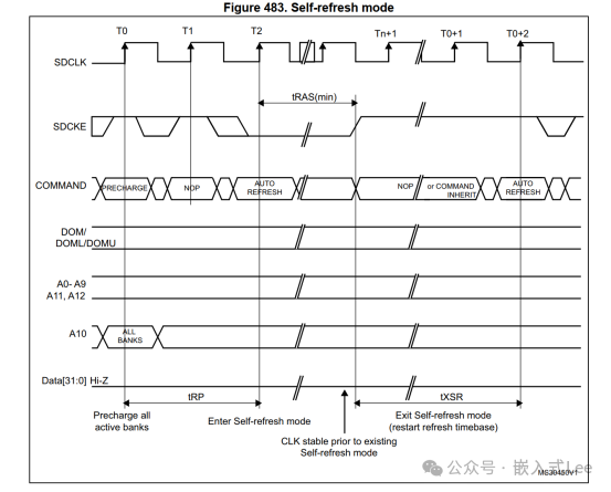
Self-refresh mode
Refresh is performed by the SDRAM chip itself to retain data without an external clock.
Note that it is the SDRAM chip that refreshes itself, not the SDRAM controller and software issuing refresh commands, and the clock is stopped at this time.
Power-down mode
Refresh is performed by the SDRAM controller. At this time, the controller needs to control the exit from power-down to perform refresh and then re-enter power-down.
This is done by the SDRAM controller.
Self-refresh Mode
By setting the mode bits to “101” and configuring in the FMC_SDCRM register (CTB1 and/or CTB2) to select which SDRAM BANK this mode is for.
The SDRAM clock stops running after the TRAS delay, and the internal refresh timer only stops counting when one of the following conditions is met:
1.Self-refresh commands are issued to both devices.
2.One of the devices is not activated (the SDRAM bank is not initialized).
Before entering self-refresh mode, the SDRAM controller automatically issues a PALL command.
If the write data FIFO is not empty, all data will be sent to memory before activating self-refresh mode, and the BUSY status flag remains set.
In self-refresh mode, all SDRAM device inputs become irrelevant except for keeping SDCKE low.
SDRAM devices must remain in self-refresh mode for at least the minimum time of TRAS, and can remain in self-refresh mode indefinitely thereafter. To ensure this minimum time, the busy status flag remains high during the TRAS delay after self-refresh activation.
Once an SDRAM device is selected, the SDRAM controller generates a series of commands to exit self-refresh mode. After memory access, the selected device remains in normal mode.
To exit self-refresh, the MODE bits must be set to “000” (normal mode), and configure CTB1 and CTB2 in the FMC_SDCMR register to determine which SDRAM BANK.
As shown in the figure:
1.At time T0, execute PALL first.
2.Then wait for tRP time.
3.At time T2, send the AUTO REFRESH command.
4.Then within tRAS time, the SDRAM chip enters self-refresh mode.
5.Within tXSR time, exit self-refresh mode.
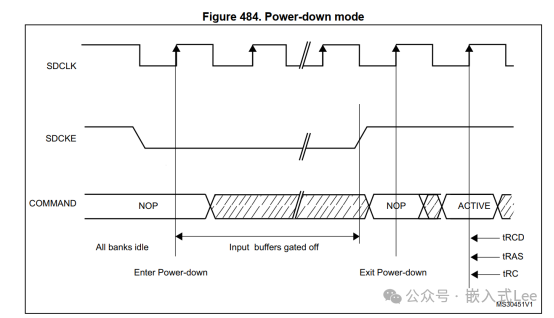
Power-down Mode
By setting the mode bits to ‘110’, configure CTB1 and CTB2 in the FMC_SDCMR register to determine which SDRAM BANK this mode is for.
If the write data FIFO is not empty, all data will be sent to memory before activating this mode.
Once an SDRAM device is selected, the SDRAM controller will exit this mode. After memory access, the selected SDRAM device remains in normal mode.
In this mode, all SDRAM device inputs and output buffers are disabled except for keeping SDCKE low.
SDRAM devices cannot remain in this mode for more than the refresh cycle, nor can they perform auto-refresh cycles themselves. Therefore, the SDRAM controller performs refresh operations by:
1.Exiting this mode, driving SDCKE high.
2.If a row is active in power-down mode, generate a PALL command; otherwise, no need.
3.Generate an auto-refresh command.
4.Drive SDCKE low again to return to Power-Down mode.
To exit Power-Down mode, the mode bits must be set to “000” (normal mode), and configure CTB1 and CTB2 in the FMC_SDCMR register to determine which SDRAM BANK.
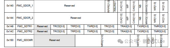
4.6 Registers
The registers are quite simple.
Each of BANK1 and BANK2 has a control register and a timing register.
The control register configures ROW, COLUMN, bus width, etc., while the timing register configures timing parameters.
However, some parameters are based on Bank1, refer to the register description for specifics.
There is a command register to control sending different commands to enter different modes.
There is also a refresh timer register to control the refresh interval.
And a status register to check refresh error status, busy status, and the mode the bank is in.
5. Conclusion
In summary, this article introduced the SDRAM controller of STM32F429, preparing for the subsequent driver writing. The key points to understand include the address space and more.