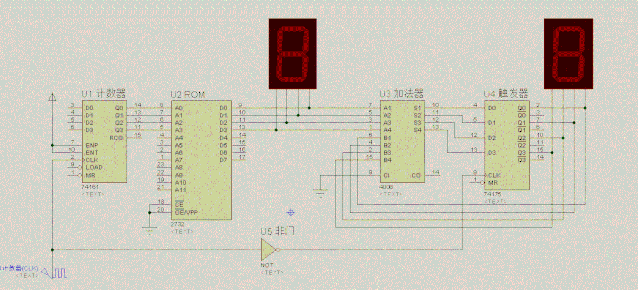
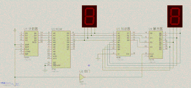
1. Appearance of the Homemade Computer
For a long time, I always struggled to understand some basic concepts and principles: What is hardware? How does hardware operate internally? What is software? Where is software? How does software run on hardware? How does hardware execute software?

|
Von Neumann Architecture |
Homemade Computer |
|
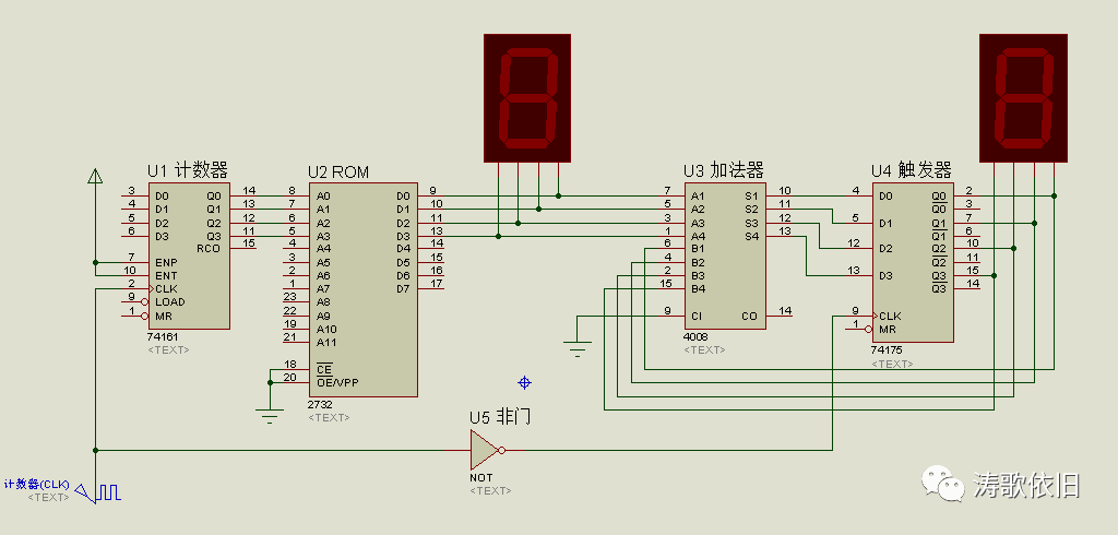
CPU Arithmetic Unit |
U3 Adder |
|
CPU Controller |
U1 Counter U4 Trigger U5 NOT Gate Clock Signal |
|
Memory |
U2 Memory |
|
Input Device |
Not Involved (Because the input has been pre-stored in U2) |
|
Output Device |
Digital Display |
2. Components of the Homemade Computer

It is easy to analyze the logical relationship:
|
S |
R |
Q |
Q’ |
|
1 |
0 |
1 |
0 |
|
0 |
1 |
0 |
1 |
|
0 |
0 |
Hold |
Hold |
|
1 |
1 |
0 |
0 |
-
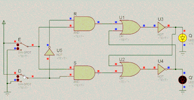
When S=0, R=0, the OR gate has no contribution, so it will not affect the circuit. At this time, Q and Q’ are opposites, one must be 0 and the other must be 1.
-
When S=1, R=1 (this input is not wrong), both Q and Q’ are 0, and we are not interested in this situation, so we can ignore it, hence we agree that S and R cannot both be 1 at the same time.
-
When ignoring the input combination of S=1, R=1, Q and Q’ are always opposites.
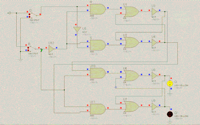
2. D Latch
Let’s look at the D latch circuit. It can use multiple devices to ensure that both inputs of the RS latch cannot be 1. In the following diagram, the outputs of R and S can never both be 1:
-
When E=0, regardless of how D changes, after passing through the two AND gates R and S, the outputs of R and S are always 0, so Q and Q’ always hold their state. -
When E=1, the outputs of R and S depend entirely on D, obviously Q=D.
-
The enable terminals of the upper and lower D latches are opposite, so regardless of whether the control switch E is 0 or 1, one of the upper and lower D latches must be invalid, preventing the D data from being saved to the Q terminal.
-
When E changes from 1 to 0, the lower D latch becomes invalid, so it cannot save the D data to the Q terminal.
-
When E changes from 0 to 1, the lower D latch becomes active, and the upper D latch becomes invalid, but the output of U4 has already captured the data from the D terminal, so while the lower D latch is active, the output data from U4 is saved to the Q terminal. Therefore, overall, when E changes from 0 to 1, it can save the D data to the Q terminal. This latching occurs only at the moment the signal transitions from 0 to 1, hence it is called a rising edge-triggered latch.
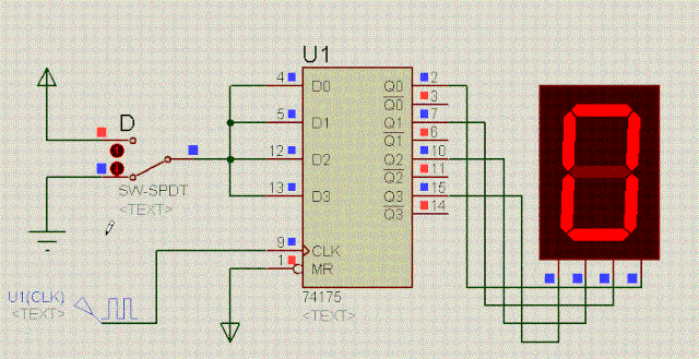
However, this D trigger is a bit complex. Let’s abstract it and directly use a packaged D trigger, as shown in the following diagram, which can be seen that it only saves D to Q when E transitions from 0 to 1.

Using a switch to provide a rising edge requires manually toggling the switch, which is very cumbersome. Can we create an automatic rising edge? Of course, we can.
We introduce a clock signal that continuously toggles between 0 and 1, thereby generating rising edges. The clock signal is simple, as shown in the animation:

Think about why the CPU needs a clock to function? This question is interesting and easy to answer from two perspectives:
-
The theoretical model of computers is the Turing machine, and the Turing machine is a finite state machine that requires a clock signal to drive state changes. -
Data in computers needs to be saved and updated in a sequential manner. Using the aforementioned trigger as an example, a rising edge signal is required to trigger it, hence the need for a clock signal.

|
n-th Second |
U1 |
U2 |
U3 |
U4 |
U4U3U2U1 |
|
0 |
0 |
0 |
0 |
0 |
0 |
|
1 |
1 |
0 |
0 |
0 |
1 |
|
2 |
0 |
1 |
0 |
0 |
2 |
|
3 |
1 |
1 |
0 |
0 |
3 |
|
4 |
0 |
0 |
1 |
0 |
4 |
|
5 |
1 |
0 |
1 |
0 |
5 |
|
6 |
0 |
1 |
1 |
0 |
6 |
|
7 |
1 |
1 |
1 |
0 |
7 |
|
8 |
0 |
0 |
0 |
1 |
8 |
|
9 |
1 |
0 |
0 |
1 |
9 |
|
10 |
0 |
1 |
0 |
1 |
A |
|
11 |
1 |
1 |
0 |
1 |
B |
|
12 |
0 |
0 |
1 |
1 |
C |
|
13 |
1 |
0 |
1 |
1 |
D |
|
14 |
0 |
1 |
1 |
1 |
E |
|
15 |
1 |
1 |
1 |
1 |
F |

000000000000000100000010000000110000010000000101
000000000000000100000010000000110000010000000101
This program is not intuitive, so for easier reading, let’s split it:
000000000000000100000010000000110000010000000101
|
U2 Input Terminal A3A2A1A0 |
U2 Output Terminal D3D2D1D0 Its specific content is related to the program we wrote |
|
0000 |
0000 |
|
0001 |
0001 |
|
0010 |
0010 |
|
0011 |
0011 |
|
0100 |
0100 |
|
0101 |
0101 |
The U1 counter on the left side of memory U2 counts from 0 to F, so when the counter reaches 3, the input terminal of U2 is exactly 3, and the data stored in U2 at this point is exactly 3.
Let’s understand the execution flow of the computer circuit by comparing it with the animation above:
|
Clock Signal |
U1 Output |
U2 Output |
U3 Output |
U4 Output
|
|
0 |
0 |
0 |
0 |
0 |
|
Rising Edge |
1 |
1 |
1 |
0 |
|
Falling Edge |
1 |
1 |
1 |
1 |
|
Rising Edge |
2 |
2 |
3 |
1 |
|
Falling Edge |
2 |
2 |
3 |
3 |
|
Rising Edge |
3 |
3 |
6 |
3 |
|
Falling Edge |
3 |
3 |
6 |
6 |
|
Rising Edge |
4 |
4 |
A |
6 |
|
Falling Edge |
4 |
4 |
A |
A |
|
Rising Edge |
5 |
5 |
F |
A |
|
Falling Edge |
5 |
5 |
F |
F |

00000000000000100000010000001000
3. Programming the Homemade Computer
The program written in 0s and 1s is called a machine language program, which runs directly on hardware. Compared to toggling circuit switches, this is already a significant improvement. However, if we keep writing programs in 0s and 1s without making any mistakes, who can endure it?
A long string of 0s and 1s is too difficult to understand; it is the language of the machine world, while humans have their own language. These two languages are not compatible, so we need to explore better ways to write programs that make it easier for humans. What to do?
Let’s look back at the machine language for 1+2+3+4+5:
000000000000000100000010000000110000010000000101
How can we reduce the difficulty for humans to write programs? We can consider writing it like this:
ORG 0000HDB 00HDB 01HDB 02HDB 03HDB 04HDB 05HEND
This language is called assembly language, and it looks much more comfortable. Now the problem is that we need a tool to convert assembly language into machine language, and this conversion tool is called an assembler, as shown in the following diagram:

Now programming has become much easier: first, write the program in assembly language, then use the assembler tool to convert the assembly language program into a machine language program.
If we want to calculate 2+4+8, we no longer have to deal with the torturous machine language of 0s and 1s; we can directly write the assembly program in assembly language as follows:
ORG 0000HDB 00HDB 02HDB 04HDB 08HEND
After conversion by the assembler tool, the above assembly language program becomes a machine language program, which is exactly the language needed by the hardware circuit, as shown below:
00000000000000100000010000001000
Then, our homemade computer executes this machine language program and gets the result as 14. However, using assembly language is still a bit awkward and not easy to understand.
Therefore, we need to abstract it further; the more abstract, the closer we get to the essence of things. To reduce programming difficulty, we optimize the programming method again, using high-level languages as follows:
int a=1+2+3+4+5;printf("%d", a);
However, the circuit does not recognize high-level languages; it only recognizes high and low levels, i.e., 1 and 0, so we also need tools to convert high-level languages. The relationship is shown below:

From the table below, we can see the comparison of machine language, assembly language, and high-level language. Clearly, programming in high-level language is easier and more intuitive:
|
Purpose |
Machine Language |
Assembly Language |
High-Level Language |
|
Calculation 1+2+3+4+5 |
000000000000000100000010000000110000010000000101 |
ORG 0000H DB 00H DB 01H DB 02H DB 03H DB 04H DB 05H END |
int a=1+2+3+4+5; printf(“%d”, a); |
|
Calculation 2+4+8 |
00000000000000100000010000001000 |
ORG 0000H DB 00H DB 02H DB 04H DB 08H END |
int a=2+4+8; printf(“%d”, a); |
-
The above assembly language is very simple and does not involve instructions, only the positions where data is stored. Some friends may think that the above assembly language instructions are pseudo-instructions, but it doesn’t matter; we still understand it as assembly language without side effects. Moreover, the machine code generated after conversion by the assembler can indeed run on the computer we made. -
The above high-level language, after conversion by general compilers and assemblers, cannot run on our homemade computer; it must go through a special compiler. We do not need to further understand this special compiler, as it is merely a conversion tool.
Okay, that’s it for now. This article will come to a close. For friends who want to understand computer principles, if you can complete the experiments in this article by yourself, it will surely deepen your understanding of computer principles. Keep it up!
More Exciting Content:
[Editorial Message] Professor Li Xiaoming from Peking University: Thoughts from the “Year of Improving Classroom Teaching”…
[Table of Contents] Computer Education, Issue 12, 2021
Notice for the 2021 China Higher Education Computer Education Conference (Sixth Round)
[Table of Contents] Computer Education, Issue 11, 2021
[Table of Contents] Computer Education, Issue 10, 2021
[Table of Contents] Computer Education, Issue 9, 2021
[Table of Contents] Computer Education, Issue 8, 2021
Professor Chen Daoqu from Nanjing University: Which is more important, teaching students to ask questions or teaching students to answer questions?
[Table of Contents] Computer Education, Issue 7, 2021
[Table of Contents] Computer Education, Issue 6, 2021
[Series of Ten Words]: Trends in Computer Discipline Development and Their Impact on Computer Education
Professor Li Xiaoming from Peking University: From Interesting Mathematics to Interesting Algorithms to Interesting Programming—A Path for Non-Major Learners to Experience Computational Thinking?
Several Thoughts on Building a First-Class Computer Discipline
Professor Liu Yunhao from Tsinghua University Answers AI Two Thousand Questions
Professor Zhan Dechen from Harbin Institute of Technology: A New Model to Ensure Teaching Quality in Colleges—Synchronous and Asynchronous Blended Teaching
[Principal Interview] Accelerating the Advancement of Computer Science Education—An Interview with Professor Zhou Aoying, Vice President of East China Normal University
New Engineering and Big Data Major Development
Learning from Others—Compilation of Research Articles on Computer Education at Home and Abroad