“ This article focuses on the ST7789V2 color TFT-LCD controller, introducing its parameters, functional components, pin definitions, control timing, and common commands. It details the hardware connection between the ESP32-S3 and this chip, program design, and displays the visual effects, providing a reference for related embedded display projects.”
01
—
Introduction
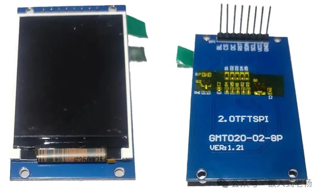
ST7789V2 is a color TFT-LCD controller/driver launched by Sitronix, designed for small size, high-resolution SPI screens. The core parameters are as follows:
·Resolution: 240×320 (backward compatible with 240×240 and other cropping modes);
·Interface: 4-wire SPI (SCK, MOSI, CS, DC), clock up to 62.5 MHz; some modules support 2-data-lane high-speed mode;
·Pixel Format: Supports RGB888 (18-bit, 3 bytes/pixel), RGB666 (18-bit, 3 bytes/pixel), and RGB565 (16-bit, 2 bytes/pixel);
·Display Type: IPS full-view, brightness 200-500 cd/m², color 262K;
·Operating Voltage: 3.3 V single power supply, backlight can be PWM dimmed;
·Typical Sizes: 1.54″, 1.9″, 2.0″, 2.2″, 2.8″, etc., module size starting from 31×34 mm.
Commonly used in smartwatches, portable instruments, IoT panels, and embedded teaching projects.
02
—
ST7789V2 Chip Introduction
1. Functional Block Diagram
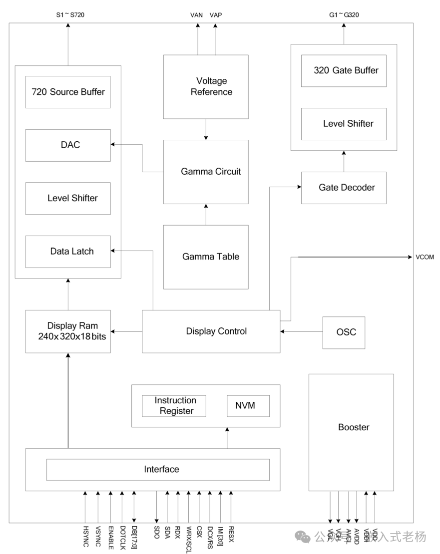
·Interface: Responsible for connecting with external controllers (such as MCU), receiving image data, commands, and synchronization signals (HSYNC, VSYNC, etc.), supporting parallel/serial communication (such as 8-bit parallel, SPI, corresponding to DB [7:0], SDA/SCL pins).
·Instruction Register and NVM: Instruction Register temporarily stores external commands (such as display mode, Gamma correction configuration); NVM (non-volatile memory) can solidify initialization parameters (such as default Gamma curve, screen offset), automatically loaded on power-up.
·Display Control: The core “dispatch center” of the chip, coordinating image caching, Gamma correction, timing synchronization, and driving source and gate signal links to work together.
·Display RAM: Capacity of 240×320×18 bits, temporarily stores image data to be displayed, matching screen resolution and color depth, serving as a data “transit station”.
·Source Driver Link: Includes Data Latch, Level Shifter, DAC, 720 Source Buffer, converting digital image data into analog voltages to drive the LCD screen source (S1~S720).
·Gamma Correction Module: Gamma Table stores correction curve parameters, Gamma Circuit compensates for the LCD screen “voltage-brightness” non-linearity based on parameters, optimizing display effects.
·Gate Driver Link: Includes Gate Decoder, Level Shifter, 320 Gate Buffer, generating scanning signals to drive the LCD screen gate (G1~G320), controlling pixel row selection.
·Power Management: Voltage Reference provides precise voltage reference (such as Gamma correction, DAC conversion); Booster generates gate drive and bias voltages (such as VGH, VGL), meeting the high voltage requirements of the LCD screen.
·Oscillator: Generates the internal working clock of the chip, synchronizing display control and data transmission timing.
The MCU writes the 240×320×18 bit image into the Display RAM at once, and the ST7789V refreshes the RAM data at a frequency of over 60 Hz, displaying the complete image on the TFT panel through 720 sources and 320 gates line by line.
2.Pin Definitions
|
Pin Group |
Pin Name |
Function Description |
|
Interface Control |
HSYNC |
Line synchronization signal, used to indicate the start of the “line” of image data, synchronizing line data transmission with the external controller |
|
VSYNC |
Field synchronization signal, indicating the start of a complete “frame” of image data, controlling the screen refresh timing |
|
|
ENABLE (or TE) |
Enable signal / tearing effect alignment signal, used to control the chip enable or synchronize screen output |
|
|
DotClock |
Pixel clock, defining the rhythm of image data transmission, ensuring data is aligned with clock edges |
|
|
DB[7:0] |
8-bit parallel data bus, used for transmitting image pixel data, command parameters (also supports serial mode adaptation) |
|
|
SPI Interface |
SDO |
Data output pin in SPI mode (if bidirectional communication is supported, can return status / read ID, etc.) |
|
SDA (or MOSI) |
Master input / slave output data pin in SPI mode, used to receive image / command data sent by the external controller |
|
|
SCL (or SCK) |
Clock pin in SPI mode, synchronizing SPI data transmission timing |
|
|
Control Commands |
D/CX (or DC) |
Data / command selection pin, high level indicates “data” transmission (such as pixels), low level indicates “command” transmission |
|
CSX (or CS) |
Chip select pin, low level enables chip communication, used to select ST7789V when multiple devices are connected in parallel |
|
|
RESET |
Reset pin, low level triggers hardware reset of the chip, used to initialize display state |
|
|
Power Related |
VDD |
Core logic power supply of the chip (usually 1.8V/3.3V, as specified in the manual) |
|
VDDIOT |
IO port power supply, providing working voltage for interface pins (such as DB [7:0], SPI pins) |
|
|
AVDD |
Analog circuit power supply, powering DAC, Gamma correction, reference voltage module, ensuring the accuracy of analog signals |
|
|
VGH |
Gate high voltage, generated by the Booster, used to turn on the row pixels of the TFT screen (Gate drive) |
|
|
VGL |
Gate low voltage, generated by the Booster, used to turn off the row pixels of the TFT screen (Gate cutoff) |
|
|
VCOM |
Common electrode voltage, providing reference bias for TFT screen pixels, stabilizing display grayscale |
|
|
Output Drive |
S1~S720 |
Source drive output, connecting to the TFT screen column electrodes, outputting analog voltages after Gamma correction and DAC conversion |
|
G1~G320 |
Gate drive output, connecting to the TFT screen row electrodes, outputting row selection scanning signals (in conjunction with source control pixels) |
|
|
Other Auxiliary |
OSC (or external crystal) |
Oscillator pin, can connect an external crystal / clock input, providing the internal working timing reference for the chip |
|
NVM Related Pins |
(Some packages may not have exposed pins, built-in non-volatile storage for solidifying initialization parameters) |
3.Control Timing
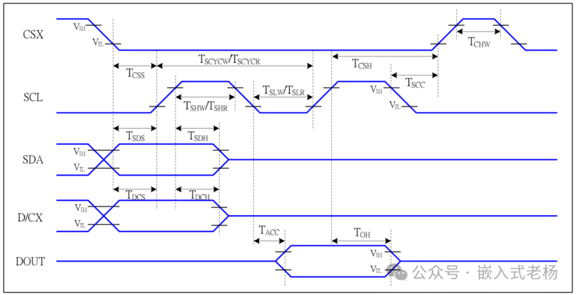
The above is the working timing diagram of the ST7789V four-wire SPI, which differs slightly from the standard SPI signal names (the standard SPI interface typically includes 4 signals: clock signal (SCK), master output slave input signal (MOSI), master input slave output signal (MISO), and chip select signal (CS)).
In the ST7789V four-wire SPI, SCL (corresponding to SCK in standard SPI, i.e., clock signal), SDA (corresponding to MOSI in standard SPI, used for the master to send data to the slave), CSX (corresponding to CS in standard SPI, chip select signal, active low), and additionally, there is the D/CX signal. The D/CX signal is used to distinguish whether the transmission is data or command, with a high level indicating data transmission (such as pixel data) and a low level indicating command transmission. This is a unique signal for the ST7789V, which does not exist in standard SPI.
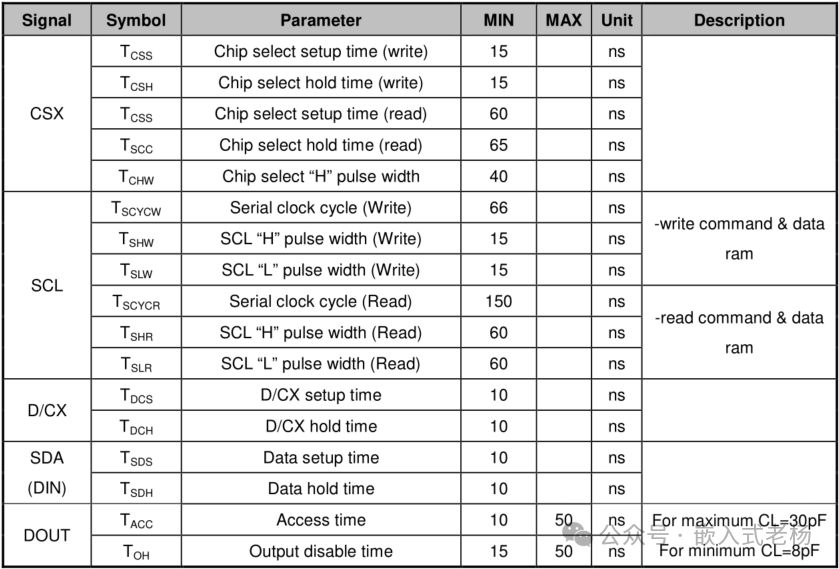
The working frequency f = 1/T, where T is the clock period. For write operations, the minimum clock period is TSCYCW, with a minimum value of 66ns. According to the frequency calculation formula, the maximum working frequency fmax = 1/66×10−9Hz ≈ 15.15MHz. This means that under the conditions that meet the timing parameter requirements specified by the ST7789V, the maximum working frequency of its four-wire SPI working timing is approximately 15.15MHz.
4. Common Command Codes
|
Function Category |
Command Code |
Name/Function |
Remarks |
|
System Control |
0x01 |
SWRESET |
Software reset, requires waiting for 120 ms |
|
0x10 |
SLEEP IN |
Enter sleep mode, screen turns off |
|
|
0x11 |
SLEEP OUT |
Wake up, requires waiting for 120 ms |
|
|
0x28 |
DISPOFF |
Turn off display (backlight not turned off) |
|
|
0x29 |
DISPON |
Turn on display |
|
|
Scan Direction |
0x36 |
MADCTL |
MX/MY/MV/RGB/BGR bit combination |
|
Pixel Format |
0x3A |
COLMOD |
Determines the width of each pixel data |
|
Window Setting |
0x2A |
CASET |
Column address (X start and end) |
|
0x2B |
RASET |
Row address (Y start and end) |
|
|
Data Write |
0x2C |
RAMWR |
Send color data |
|
Gamma/Power |
0xB0~0xC6, 0xE0~0xE1 |
See data sheet for details |
Factory recommended values can be used directly |
Control Steps Under Different Operating Modes
Initialization Mode:
-
Send software reset command
<span><span>0x01</span></span>, wait for the chip reset to complete (usually takes a few milliseconds). -
Send exit sleep mode command
<span><span>0x11</span></span>, wait for the chip to initialize (may take a few hundred milliseconds). -
Set display direction, such as sending command
<span><span>0x36</span></span>, parameter set to<span><span>0x00</span></span>(default direction). -
Set color mode, send command
<span><span>0x3A</span></span>, parameter set to<span><span>0x05</span></span>(RGB565 mode). -
Perform Gamma curve settings, for example, send
<span><span>0xB0</span></span>and corresponding Gamma parameter values to optimize display color and brightness. -
Send display on command
<span><span>0x29</span></span>, light up the screen.
Display Content Update Mode:
-
Use
<span><span>0x2A</span></span>command to set the column address range to be updated, first send the command code, then send the high 8 bits and low 8 bits address values. -
Use
<span><span>0x2B</span></span>command to set the row address range to be updated, similarly first send the command code, then send the high 8 bits and low 8 bits address values. -
Send write display data command
<span><span>0x2C</span></span>, then according to the set row and column address area, sequentially write the color data of the pixels (in RGB565 mode, each pixel data is 16 bits).
Change Display Direction Mode:
-
Send set display direction command
<span><span>0x36</span></span>, set parameters as needed, for example, to rotate the screen 90°, set the parameter to<span><span>0x60</span></span>. -
(Optional) If the row and column address range needs to be readjusted to adapt to the new direction after changing the display direction, you can use
<span><span>0x2A</span></span>and<span><span>0x2B</span></span>commands to set the new row and column address range. -
If there are residual or abnormal displays, you can choose to rewrite the display data, using
<span><span>0x2C</span></span>command to update the screen content.
Energy Saving Mode (Sleep Mode):
-
Send enter sleep mode command
<span><span>0x10</span></span>, at this time the chip reduces power consumption, the screen display stops updating, entering low power state.
Restore Normal Display Mode (Wake from Sleep Mode):
-
Send exit sleep mode command
<span><span>0x11</span></span>, wait for the chip to recover from sleep mode (requires some time for initialization). -
Check the display status, if the display direction, color mode, and other parameters change, you can resend the corresponding commands for settings, such as
<span><span>0x36</span></span>(set display direction),<span><span>0x3A</span></span>(set color mode), etc. -
Send display on command
<span><span>0x29</span></span>, restore screen display function.
03
—
Hardware Connection
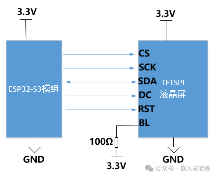
The ESP32-S3 and ST7789V2 TFT-SPI screen only require 8 wires: 3V3 for VCC and BL, GND for common ground, GPIO9-SCK, GPIO10 for SPI clock/data, GPIO46-CS, GPIO11-DC, GPIO12-RST for chip select, command, and reset, with 3.3 V levels directly compatible, sharing ground. The hardware wiring physical diagram is shown below: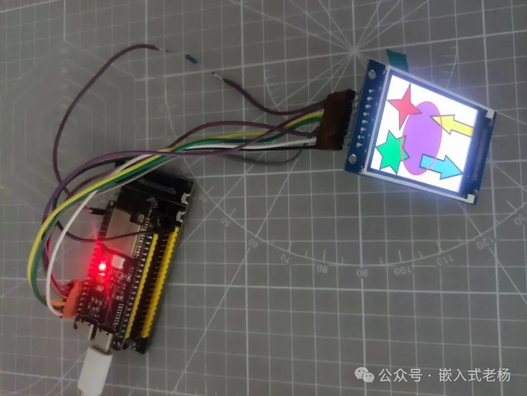
04
—
Program Design
1.GPIO Initialization
The TFTSPI LCD screen interface and GPIO connection relationship are as follows:
GPIO46 - CS;GPIO9 - SCK;GPIO10 - SDA;GPIO11 - DC;GPIO12 - RST.Among them, CS, SCK, DC, and RST are set to normal output mode, and SDA is set to input/output mode. Internal pull-up and pull-down are enabled, and the initial level is set to high.
tftspi.c
void IO_init(void){ gpio_config_t gpio_init_struct = {0};
/* CS */ gpio_init_struct.intr_type = GPIO_INTR_DISABLE; /* Disable pin interrupt */ gpio_init_struct.mode = GPIO_MODE_OUTPUT; /* Output mode */ gpio_init_struct.pull_up_en = GPIO_PULLUP_ENABLE; /* Enable pull-up */ gpio_init_struct.pull_down_en = GPIO_PULLDOWN_ENABLE; /* Enable pull-down */ gpio_init_struct.pin_bit_mask = 1ull << CS_GPIO_PIN; /* Set the pin bit mask */ gpio_config(&gpio_init_struct); /* Configure GPIO */ SPI_CS_1; /* Initialize set to 1 */ /* SCK */ gpio_init_struct.intr_type = GPIO_INTR_DISABLE; /* Disable pin interrupt */ gpio_init_struct.mode = GPIO_MODE_OUTPUT; /* Output mode */ gpio_init_struct.pull_up_en = GPIO_PULLUP_ENABLE; /* Enable pull-up */ gpio_init_struct.pull_down_en = GPIO_PULLDOWN_ENABLE; /* Enable pull-down */ gpio_init_struct.pin_bit_mask = 1ull << SCK_GPIO_PIN; /* Set the pin bit mask */ gpio_config(&gpio_init_struct); /* Configure GPIO */ SPI_SCK_1; /* Initialize set to 1 */ /* SDA */ gpio_init_struct.intr_type = GPIO_INTR_DISABLE; /* Disable pin interrupt */ gpio_init_struct.mode = GPIO_MODE_INPUT_OUTPUT; /* Input/output mode */ gpio_init_struct.pull_up_en = GPIO_PULLUP_ENABLE; /* Enable pull-up */ gpio_init_struct.pull_down_en = GPIO_PULLDOWN_ENABLE; /* Enable pull-down */ gpio_init_struct.pin_bit_mask = 1ull << SDA_GPIO_PIN; /* Set the pin bit mask */ gpio_config(&gpio_init_struct); /* Configure GPIO */ SPI_SDA_1; /* Initialize set to 1 */ /* DC */ gpio_init_struct.intr_type = GPIO_INTR_DISABLE; /* Disable pin interrupt */ gpio_init_struct.mode = GPIO_MODE_OUTPUT; /* Output mode */ gpio_init_struct.pull_up_en = GPIO_PULLUP_ENABLE; /* Enable pull-up */ gpio_init_struct.pull_down_en = GPIO_PULLDOWN_ENABLE; /* Enable pull-down */ gpio_init_struct.pin_bit_mask = 1ull << DC_GPIO_PIN; /* Set the pin bit mask */ gpio_config(&gpio_init_struct); /* Configure GPIO */ SPI_DC_1; /* Initialize set to 1 */ /* RST */ gpio_init_struct.intr_type = GPIO_INTR_DISABLE; /* Disable pin interrupt */ gpio_init_struct.mode = GPIO_MODE_OUTPUT; /* Output mode */ gpio_init_struct.pull_up_en = GPIO_PULLUP_ENABLE; /* Enable pull-up */ gpio_init_struct.pull_down_en = GPIO_PULLDOWN_ENABLE; /* Enable pull-down */ gpio_init_struct.pin_bit_mask = 1ull << RST_GPIO_PIN; /* Set the pin bit mask */ gpio_config(&gpio_init_struct); /* Configure GPIO */ SPI_RST_1; /* Initialize set to 1 */}2.LED Initialization
This case modifies the initialization process provided by the official, with the main differences in pixel format and row/column address range. The specific process is as follows:
-
Hardware reset: pull down the RST pin for 1000 ms, then pull it high and hold for 1000 ms.
-
Exit sleep: send 0x11 and delay 120 ms to fully wake the chip.
-
Set column address range: 0x2A gives 0x00 0x00 0x00 0xEF, locking X = 0~239.
-
Set row address range: 0x2B gives 0x00 0x28 0x01 0x17, locking Y = 40~279.
-
Configure Porch parameters: 0xB2 continuously writes 0x0C 0x0C 0x00 0x33 0x33, setting front and back shoulder blank.
-
Turn off display inversion: send 0x20 to maintain normal polarity.
-
Set Gate control: 0xB7 writes 0x56 to adjust VGH/VGL.
-
Set VCOMS: 0xBB writes 0x18 to set common voltage.
-
Set LCM control: 0xC0 writes 0x2C to configure source/gate drive.
-
Enable VDV/VRH: 0xC2 writes 0x01 to turn on voltage regulation.
-
Set VRH voltage: 0xC3 writes 0x1f to set reference level.
-
Set VDV voltage: 0xC4 writes 0x20 to set VCOM amplitude.
-
Set frame rate: 0xC6 writes 0x0f to achieve approximately 60 Hz.
-
Set power control: 0xD0 writes 0xA6 0xA1 to turn on AVDD/AVEE.
-
Configure positive Gamma: 0xE0 continuously writes 15 bytes of curve table.
-
Configure negative Gamma: 0xE1 continuously writes 15 bytes of curve table.
-
Set memory access direction: 0x36 writes 0x00 to maintain default scanning order.
-
Set pixel format: 0x3A writes 0x66 to enable RGB666 (18-bit).
-
Open dual-line SPI: 0xE7 writes 0x00 to enable 2-data-lane mode.
-
Turn on display inversion: send 0x21.
-
Turn on display: send 0x29 to truly light up the screen.
-
Start memory writing: send 0x2C to complete initialization, waiting for image data.
ftfspi.c
void OLED_init(void)                ////ST7789V2  {    SPI_SCK_0;    SPI_RST_0;    vTaskDelay(1000);    SPI_RST_1;    vTaskDelay(1000);    TFT_SEND_CMD(0x11);             //Sleep Out    vTaskDelay(120);               //DELAY120ms     //--------------------------------ST7789V2Frame rate setting----------------------------------//     TFT_SEND_CMD(0x2a);         //Column address set    TFT_SEND_DATA(0x00);         //start column    TFT_SEND_DATA(0x00);        TFT_SEND_DATA(0x00);        //end column    TFT_SEND_DATA(0xef);
    TFT_SEND_CMD(0x2b);         //Row address set    TFT_SEND_DATA(0x00);         //start row    TFT_SEND_DATA(0x28);     TFT_SEND_DATA(0x01);        //end row    TFT_SEND_DATA(0x17);
    TFT_SEND_CMD(0xb2);         //Porch control    TFT_SEND_DATA(0x0c);     TFT_SEND_DATA(0x0c);     TFT_SEND_DATA(0x00);     TFT_SEND_DATA(0x33);     TFT_SEND_DATA(0x33);
    TFT_SEND_CMD(0x20);         //Display Inversion Off
    TFT_SEND_CMD(0xb7);         //Gate control    TFT_SEND_DATA(0x56);           //35//---------------------------------ST7789V2 Power setting--------------------------------------//     TFT_SEND_CMD(0xbb); //VCOMS Setting    TFT_SEND_DATA(0x18);  //1f
    TFT_SEND_CMD(0xc0);         //LCM Control    TFT_SEND_DATA(0x2c);
    TFT_SEND_CMD(0xc2);         //VDV and VRH Command Enable    TFT_SEND_DATA(0x01);
    TFT_SEND_CMD(0xc3); //VRH Set    TFT_SEND_DATA(0x1f); //12
    TFT_SEND_CMD(0xc4);             //VDV Setting    TFT_SEND_DATA(0x20);
    TFT_SEND_CMD(0xc6);             //FR Control 2    TFT_SEND_DATA(0x0f); //TFT_SEND_CMD(0xca); //TFT_SEND_DATA(0x0f); //TFT_SEND_CMD(0xc8); //TFT_SEND_DATA(0x08); //TFT_SEND_CMD(0x55); //TFT_SEND_DATA(0x90);     TFT_SEND_CMD(0xd0);  //Power Control 1    TFT_SEND_DATA(0xa6);   //a4    TFT_SEND_DATA(0xa1); //--------------------------------ST7789V2 gamma setting---------------------------------------//
    TFT_SEND_CMD(0xe0);     TFT_SEND_DATA(0xd0);     TFT_SEND_DATA(0x0d);     TFT_SEND_DATA(0x14);     TFT_SEND_DATA(0x0b);     TFT_SEND_DATA(0x0b);     TFT_SEND_DATA(0x07);     TFT_SEND_DATA(0x3a);      TFT_SEND_DATA(0x44);     TFT_SEND_DATA(0x50);     TFT_SEND_DATA(0x08);     TFT_SEND_DATA(0x13);     TFT_SEND_DATA(0x13);     TFT_SEND_DATA(0x2d);     TFT_SEND_DATA(0x32);
    TFT_SEND_CMD(0xe1);                 //Negative Voltage Gamma Contro    TFT_SEND_DATA(0xd0);     TFT_SEND_DATA(0x0d);     TFT_SEND_DATA(0x14);     TFT_SEND_DATA(0x0b);     TFT_SEND_DATA(0x0b);     TFT_SEND_DATA(0x07);     TFT_SEND_DATA(0x3a);     TFT_SEND_DATA(0x44);     TFT_SEND_DATA(0x50);     TFT_SEND_DATA(0x08);     TFT_SEND_DATA(0x13);     TFT_SEND_DATA(0x13);     TFT_SEND_DATA(0x2d);     TFT_SEND_DATA(0x32);
    TFT_SEND_CMD(0x36);             //Memory data access control    TFT_SEND_DATA(0x00);
    TFT_SEND_CMD(0x3A);             //Interface pixel format    //TFT_SEND_DATA(0x55);            //65K        TFT_SEND_DATA(0x66);            //262K  RGB 6 6 6
    TFT_SEND_CMD(0xe7);             //SPI2 enable    Enable dual-line SPI (Dual-SPI) mode    TFT_SEND_DATA(0x00);

TFT_SEND_CMD(0x21); //Display inversion on TFT_SEND_CMD(0x29); //Display on TFT_SEND_CMD(0x2C); //Memory write }3.Color Test
tftspi.c
/* Red, Orange, Yellow, Green, Cyan, Blue, Purple, Black, White */  void OLED_Color_test(void)  {    unsigned int ROW,column;      TFT_SEND_CMD(0x2a);         //Column address set    TFT_SEND_DATA(0x00);         //start column    TFT_SEND_DATA(0x00);     TFT_SEND_DATA(0x00);        //end column    TFT_SEND_DATA(0xEF);
    TFT_SEND_CMD(0x2b);         //Row address set    TFT_SEND_DATA(0x00);         //start row    TFT_SEND_DATA(0x00);     TFT_SEND_DATA(0x00);        //end row    TFT_SEND_DATA(0x23);      TFT_SEND_CMD(0x2C);            //Memory write    for(ROW=0;ROW<35;ROW++)             //ROW loop    {         for(column=0;column<OLED_COLUMN_NUMBER ;column++)    //column loop        {          TFT_SEND_DATA(RED>>16);          TFT_SEND_DATA(RED>>8);          TFT_SEND_DATA(RED);        }    }    ……  //The above is red, other colors follow the same method}
4.Image Display
tftspi.c
void Picture_display(const unsigned char *ptr_pic)  {    unsigned int ROW,column;    TFT_SEND_CMD(0x2a);         //Column address set    TFT_SEND_DATA(0x00);         //start column    TFT_SEND_DATA(0x00);     TFT_SEND_DATA(0x00);        //end column    TFT_SEND_DATA(0xEF);    //0xEF
    TFT_SEND_CMD(0x2b);         //Row address set    TFT_SEND_DATA(0x00);         //start row    TFT_SEND_DATA(0x00);     TFT_SEND_DATA(0x01);        //end row    TFT_SEND_DATA(0x3F);    TFT_SEND_CMD(0x2C);            //Memory write
for(ROW=0;ROW<OLED_LINE_NUMBER;ROW++) //ROW loop OLED_LINE_NUMBER { for(column=0;column<OLED_COLUMN_NUMBER;column++) //column loop OLED_COLUMN_NUMBER { TFT_SEND_DATA(*ptr_pic++); TFT_SEND_DATA(*ptr_pic++); TFT_SEND_DATA(*ptr_pic++); } } }5.Text Display
tftspi.c
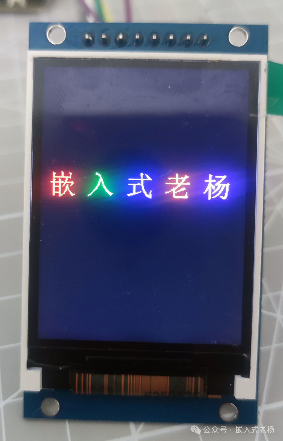
void display_char32_32(unsigned int x, unsigned int y, unsigned long color, const unsigned char *point){    unsigned int row, col, k;    unsigned char tmp, mask;
    /* 1. Set window to 32×32 */    TFT_SEND_CMD(0x2A);         /* Column address set */    TFT_SEND_DATA(x >> 8);    TFT_SEND_DATA(x);    TFT_SEND_DATA((x + 31) >> 8);    TFT_SEND_DATA(x + 31);
    TFT_SEND_CMD(0x2B);         /* Row address set */    TFT_SEND_DATA(y >> 8);    TFT_SEND_DATA(y);    TFT_SEND_DATA((y + 31) >> 8);    TFT_SEND_DATA(y + 31);
    TFT_SEND_CMD(0x2C);         /* Memory write */
    /* 2. Output 128 bytes row by row */    for (row = 0; row < 32; row++)          /* 32 rows */    {        for (col = 0; col < 4; col++)       /* 4 bytes per row */        {            tmp = *point++;                 /* Get 1 byte */            /* 3. From bit0 to bit7 corresponds to 8 pixels from left to right */            for (k = 0; k < 8; k++)            {                if (tmp & (1 << k))                {                    TFT_SEND_DATA(color >> 16);   /* R */                    TFT_SEND_DATA(color >> 8);    /* G */                    TFT_SEND_DATA(color);         /* B */                }                else                {                    TFT_SEND_DATA(0);             /* Background color = Black */                    TFT_SEND_DATA(0);                    TFT_SEND_DATA(0);                }            }        }    }}
05
—
Display Effects
1. Color Display
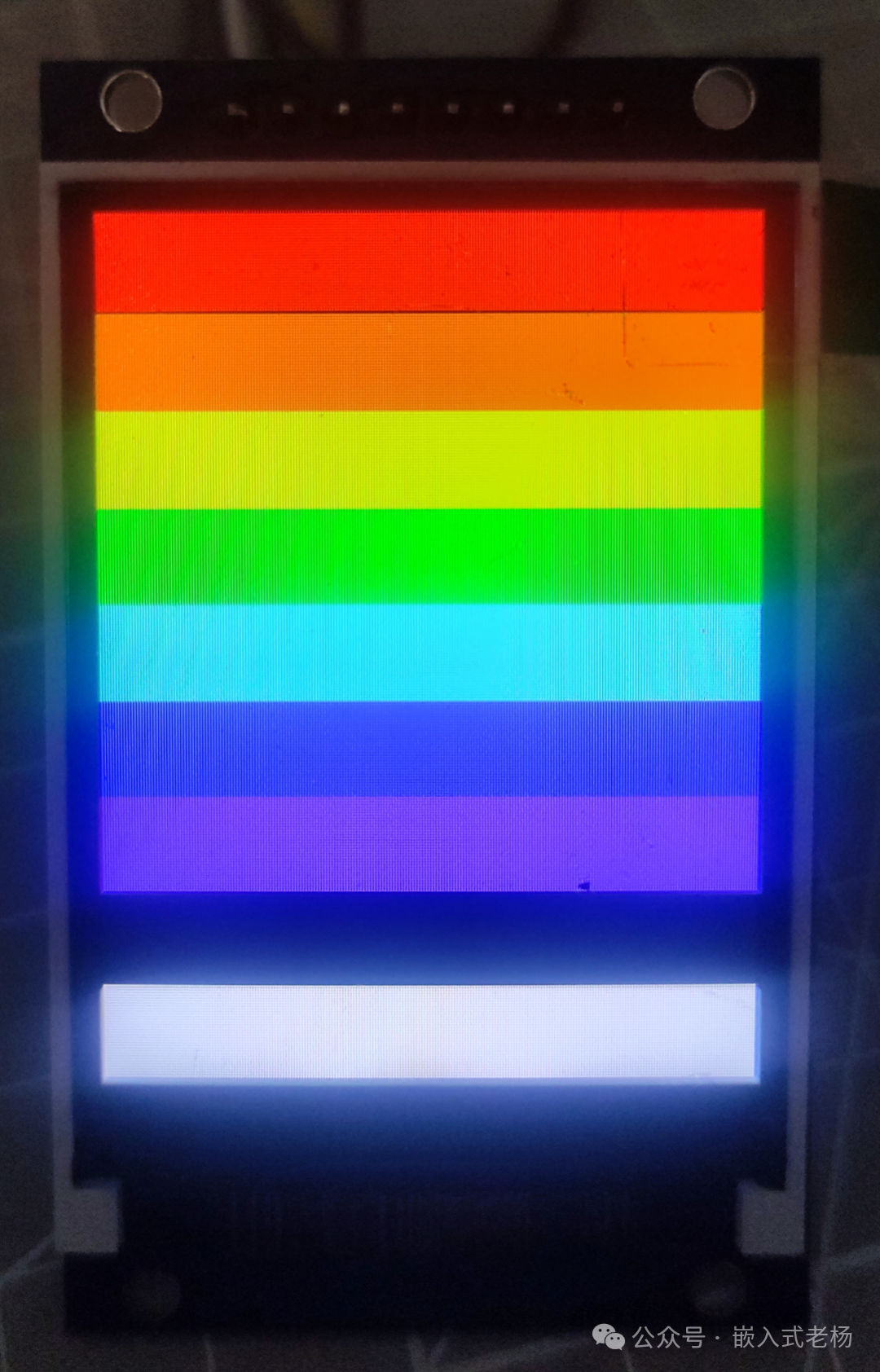
2. Text Display
3. Image Display
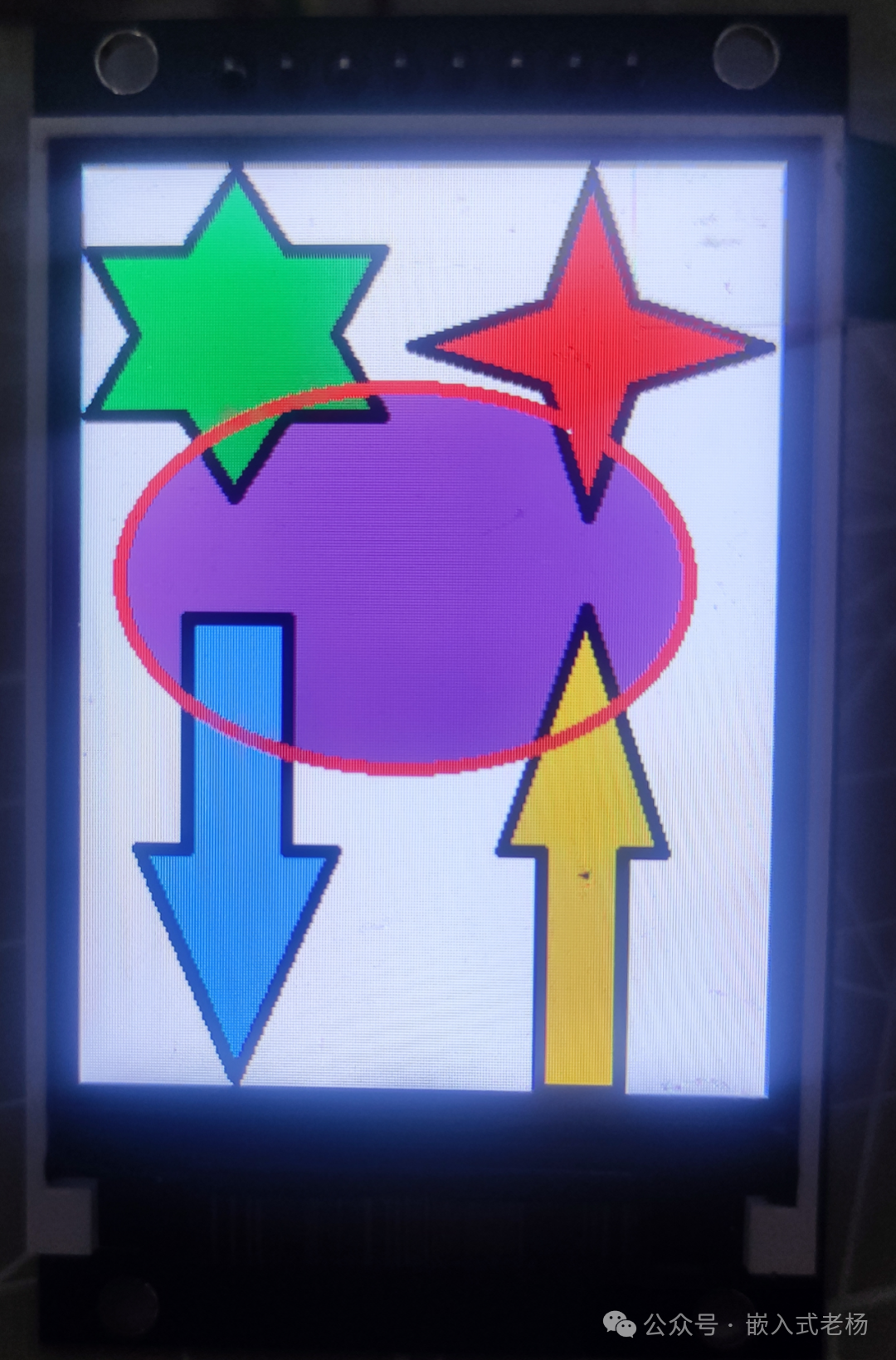
06
—
Code Link
Project code link:
https://gitee.com/ylm1101111/esp32_tftspi_lcd.git
This article’s case uses the following software and hardware:
1. SOC Model: ESP32-S3-N16R8;
2. Software Development Environment: ESP-IDF 5.3.1, VSCode IDE (VSCodeUserSetup-x64-1.102.1 version);
3. ESP32 Project Version: IDF version or Arduino version (FreeRTOS);
4. Program Download: Type C USB (USB to serial) interface;
5. This software and hardware case is for personal learning only and may not be used for commercial purposes.
References for this article:
“ESP32-S3 Technical Reference Manual Version 1.7”;
“ESP32-S3 Series Chip Technical Specification Version 2.0”.