Recently, I analyzed Yushu Technology’s L1 LiDAR: “Snow Ridge · Disassembly and Principle Analysis of Yushu Technology’s L1 LiDAR“.
Among them, the chips on the circuit board lack silkscreen printing, making it difficult to understand their specific functions.
Therefore, I asked experts from the chip company to perform a decap on the main chips to gain further insights into the chip information. This article shares the relevant results for reference.
This time, 13 chips were decapped, but unfortunately, only one had a clear model, while the others lacked obvious model markings. Thus, I can only speculate on the chip functions based on the photos, and I welcome corrections from relevant chip experts.
01
Chip Decap
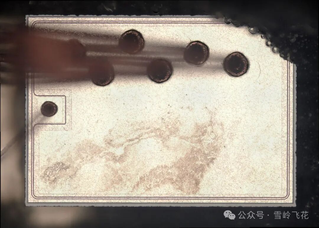
Chip decap (Decap) is also known as chip unsealing or chip cap removal. It refers to the process of partially treating a fully packaged chip (e.g., chemical etching, mechanical, laser, plasma, etc.) to remove the covering structure, exposing the internal die, bond pads, bond wires, and even leads, preparing for subsequent failure analysis, functional analysis, electrical testing, etc.
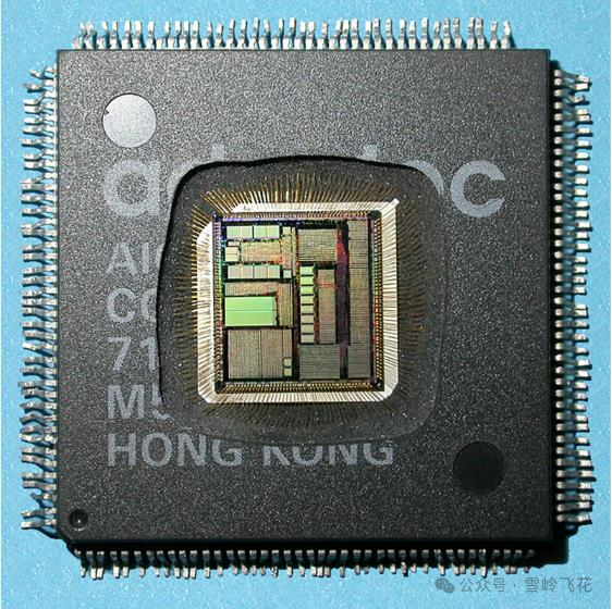
Image Source: Internet
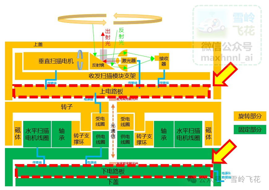
The main analysis focuses on two primary circuit boards of the Yushu LiDAR L1: the “upper circuit board” and the “lower circuit board”:
Follow and star eefocus for updates.
Scan to reply“Chip,Trial” to receive reports and join the community.

02
Lower Circuit Board
Overview of the decapped chips and their main functions on the lower circuit board:
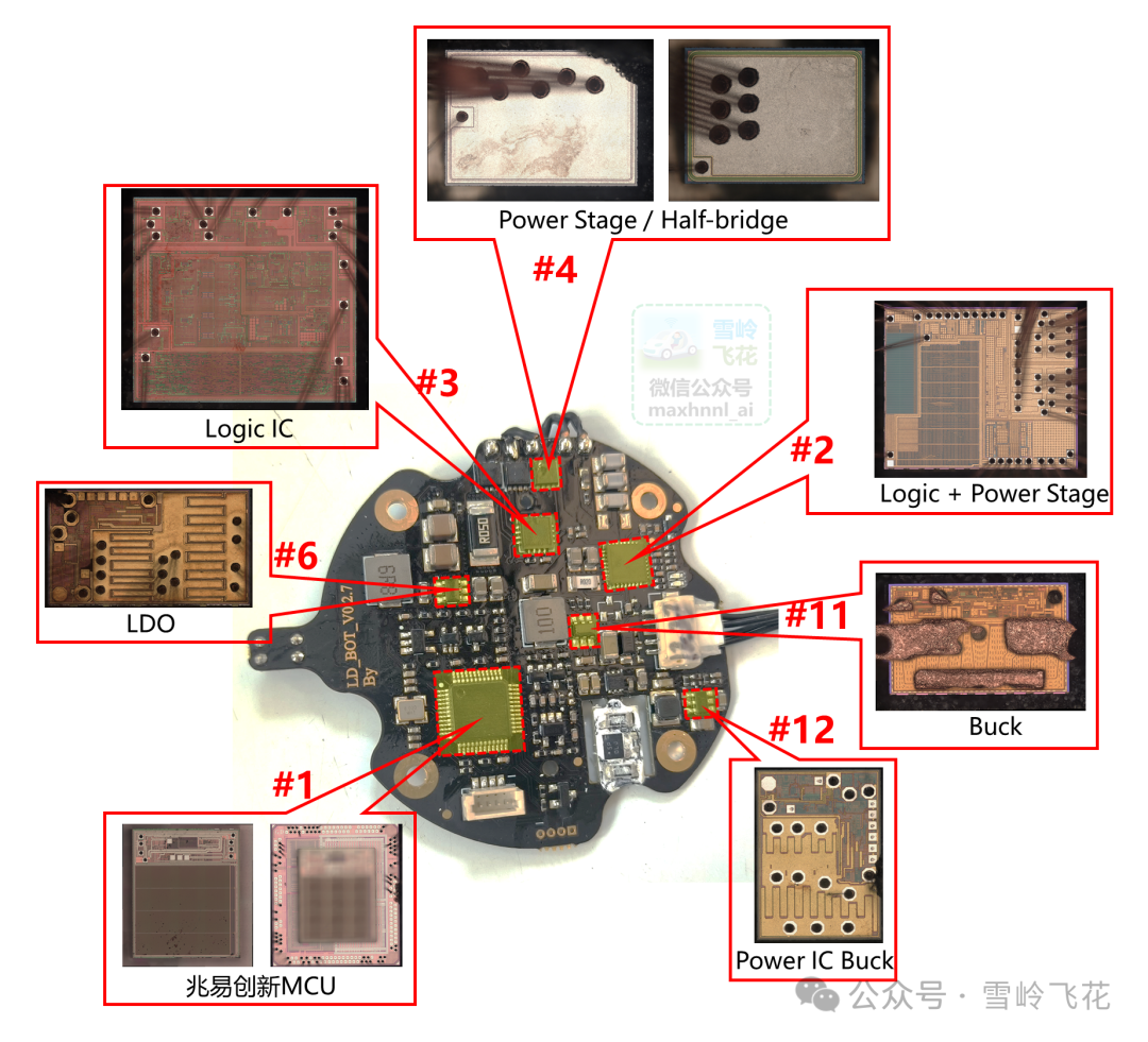
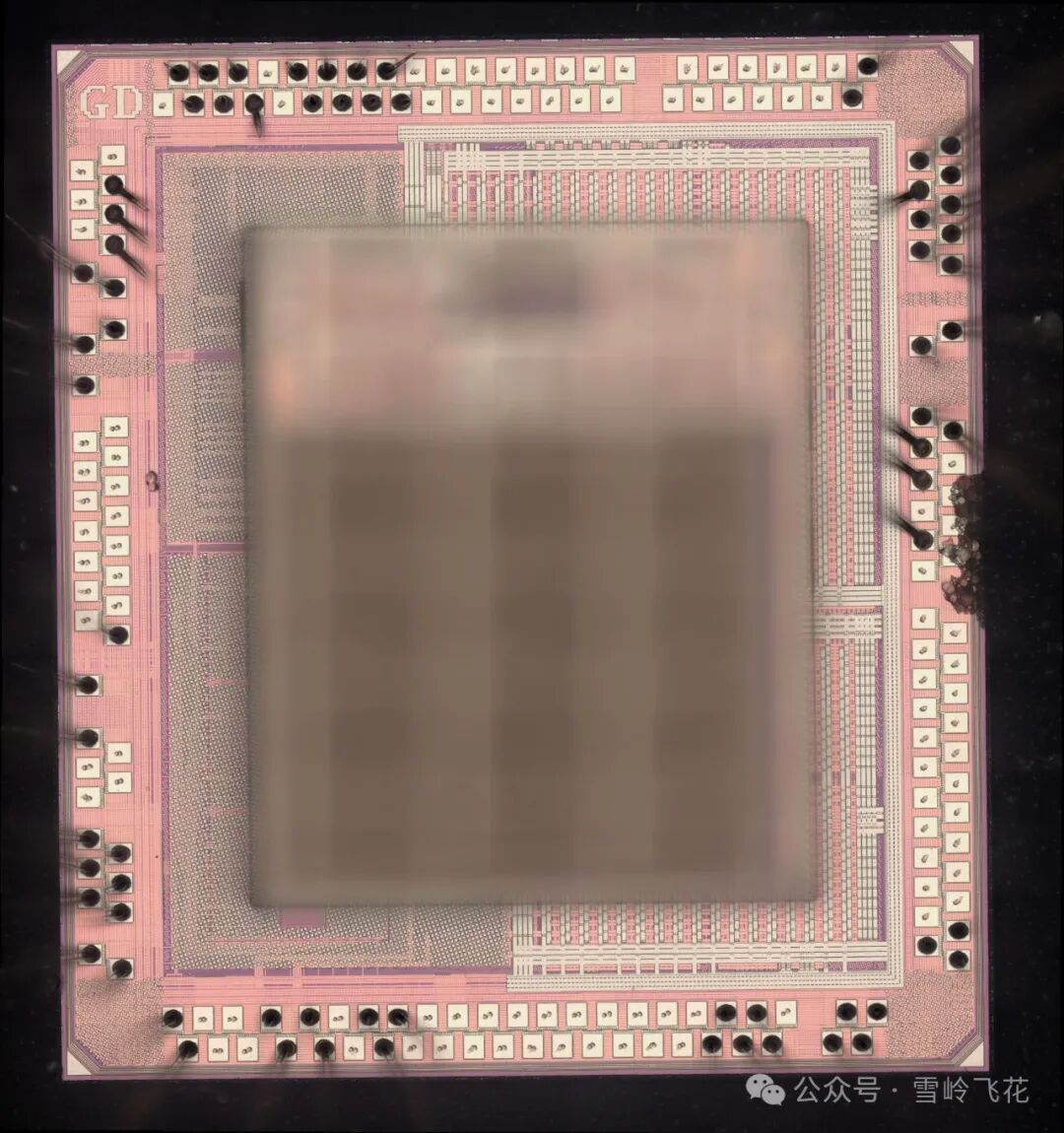
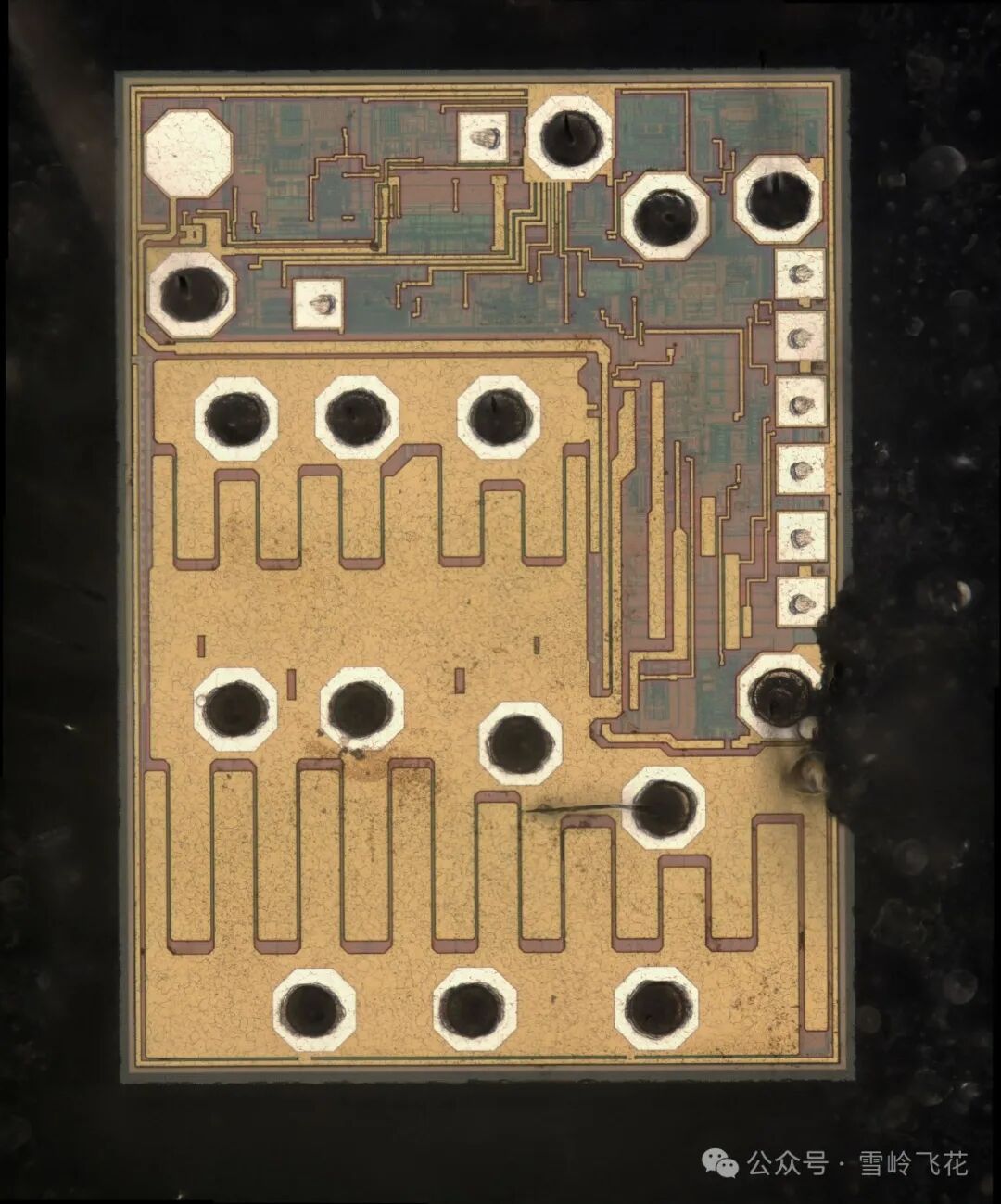
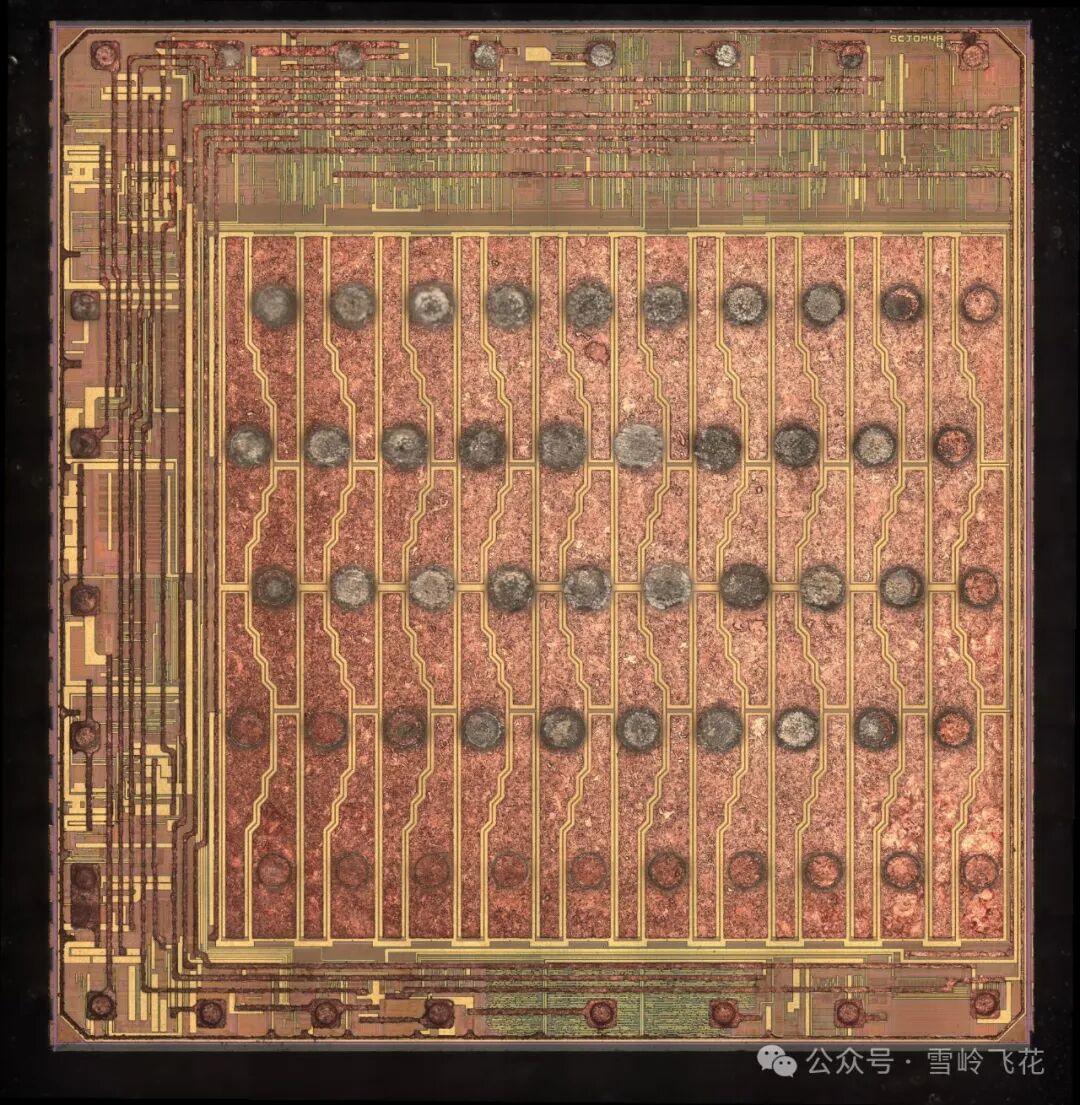
1. Chip #1
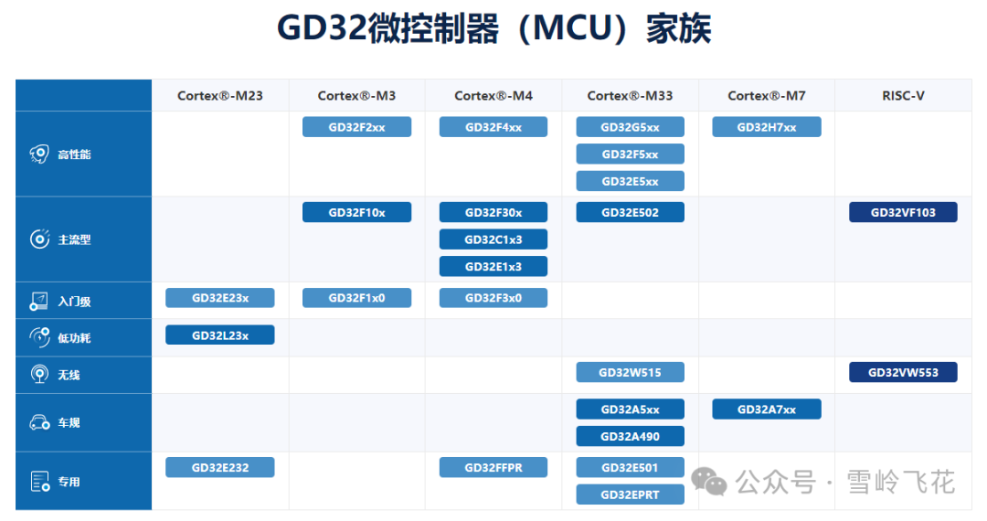
Chip #1 is a processor from GigaDevice, integrating the MCU and memory together.
The MCU part (the middle part is not clearly photographed due to focus issues):
Memory part:
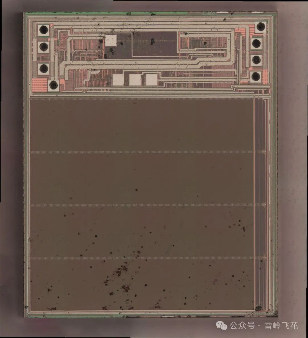
Below is the GD32 series MCU from GigaDevice, this chip should be one of their products:
2. Power Management
Chips #6, #11, and #12 are Buck and LDO, primarily for power management.
1) Chip #6
Speculated to be an LDO:
2) Chip #11
Speculated to be a Buck:
3) Chip #12
Speculated to be another Buck:
3. Motor Control
Chips #6, #11, and #12 are Buck and LDO, primarily for power management.
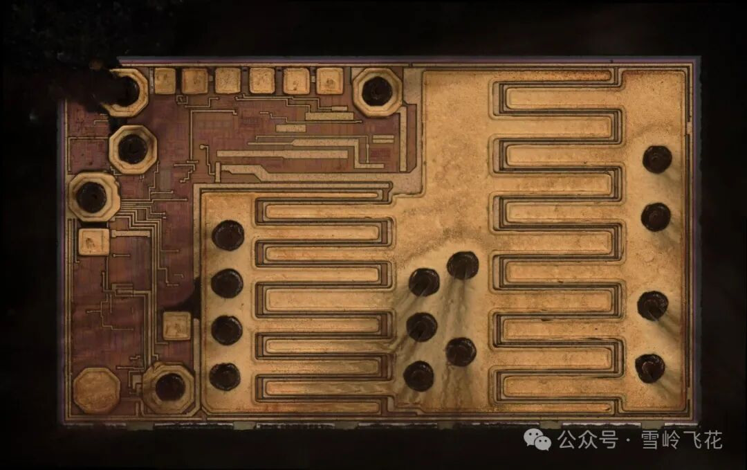
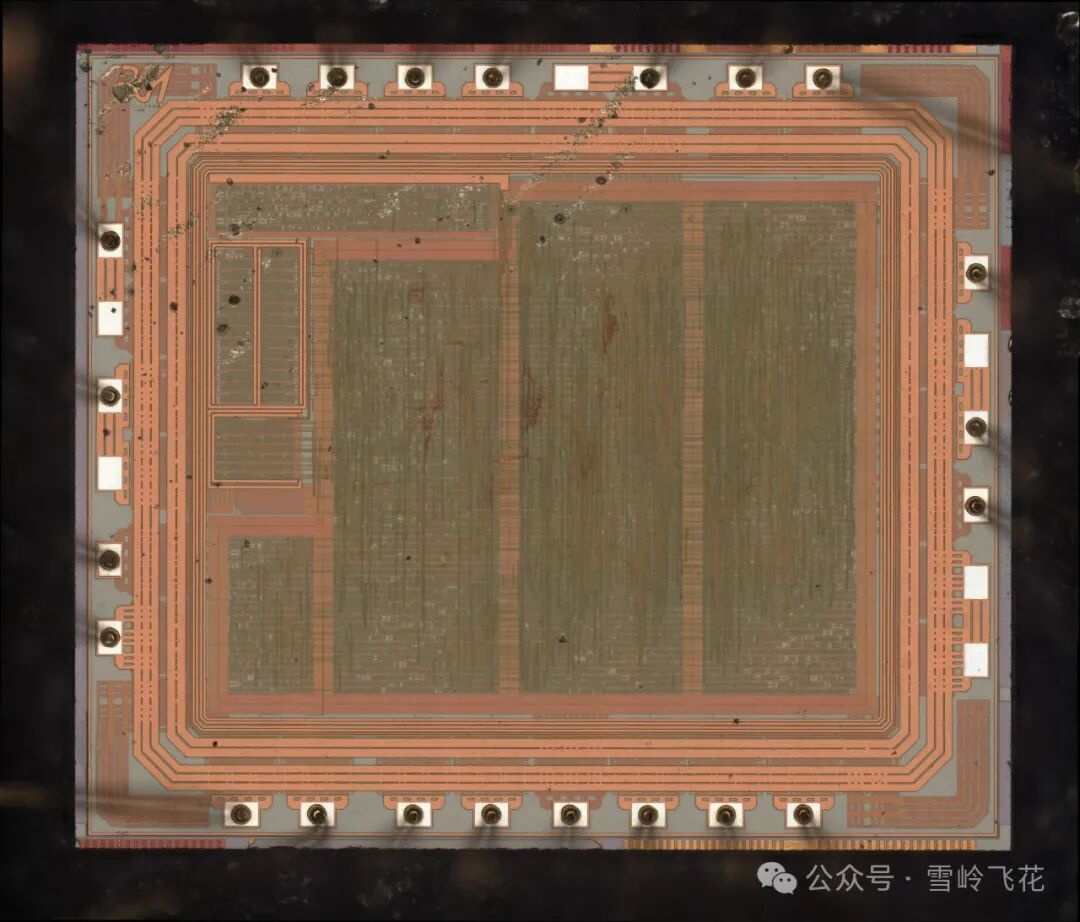
1) Chip #2
Speculated to be related to motor control logic circuits and Power Stage, mainly used for motor control and drive.
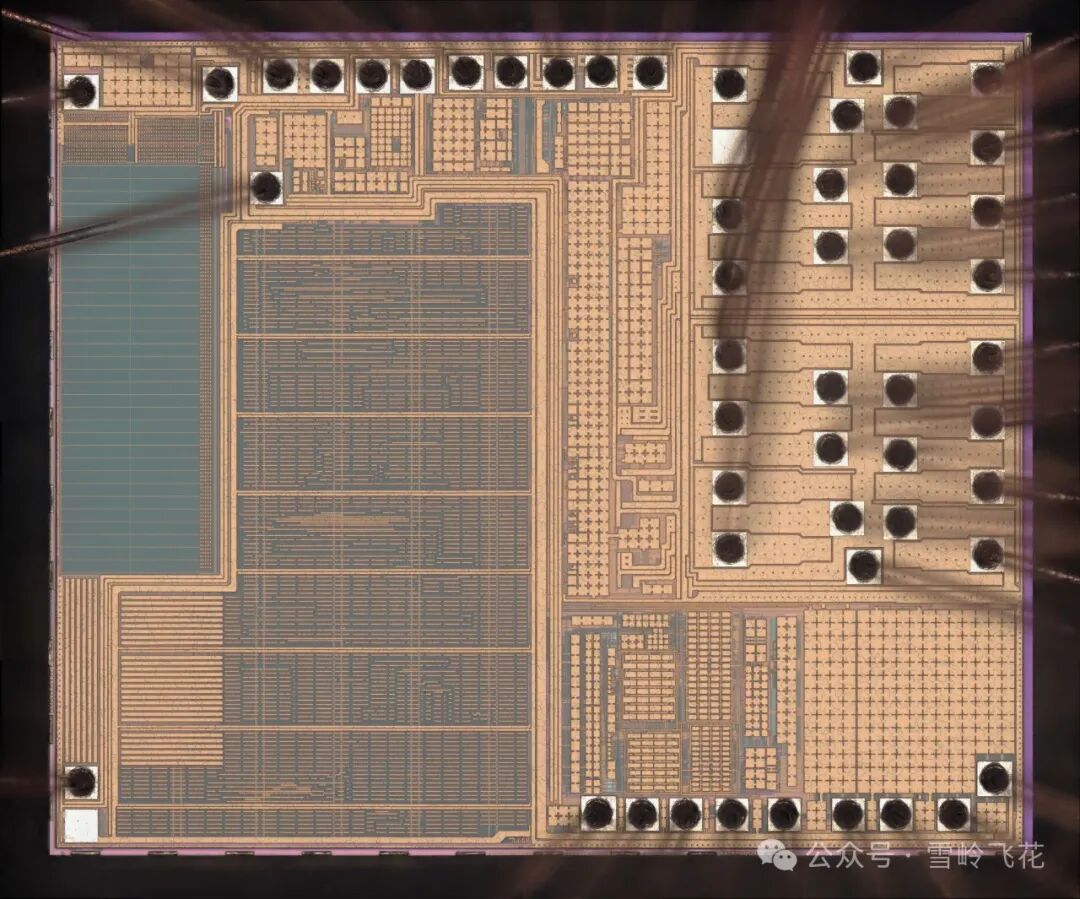
2) Chip #3
This is a logic chip, speculated to be related to motor control.
Follow and star eefocus for updates.
Scan to reply “Trial” to join the board trial group and participate in activities.
3) Chip #4
Speculated to be a half-bridge chip for motor driving:
03
Upper Circuit Board
Overview of the decapped chips and their main functions on the upper circuit board:
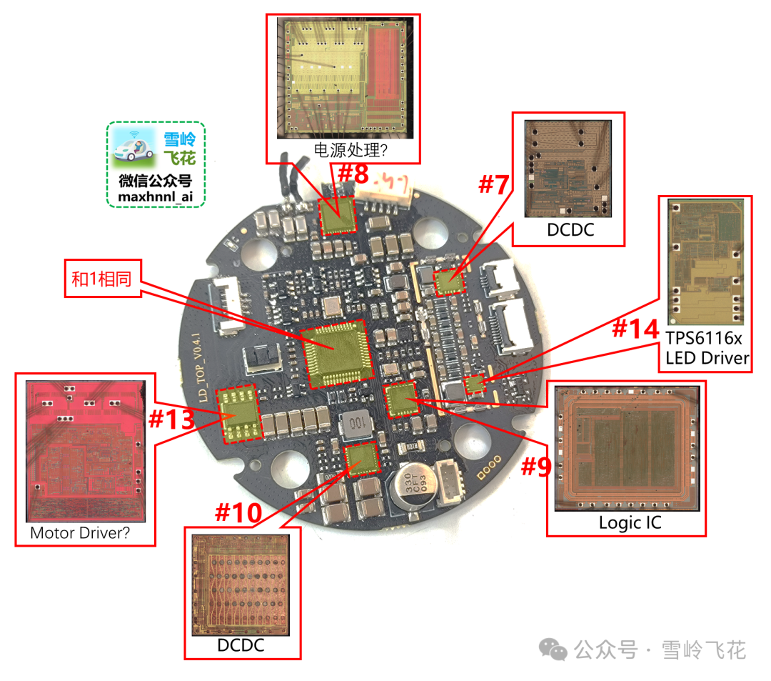
The main chip located in the center is the same as chip #1 on the lower circuit board, which is from GigaDevice.
1. Power Management
Chips #7, #8, and #10 are speculated to be for power management.
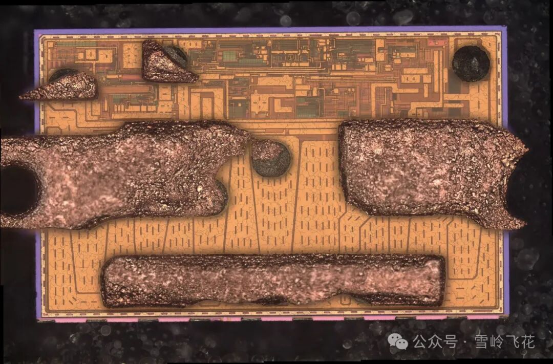
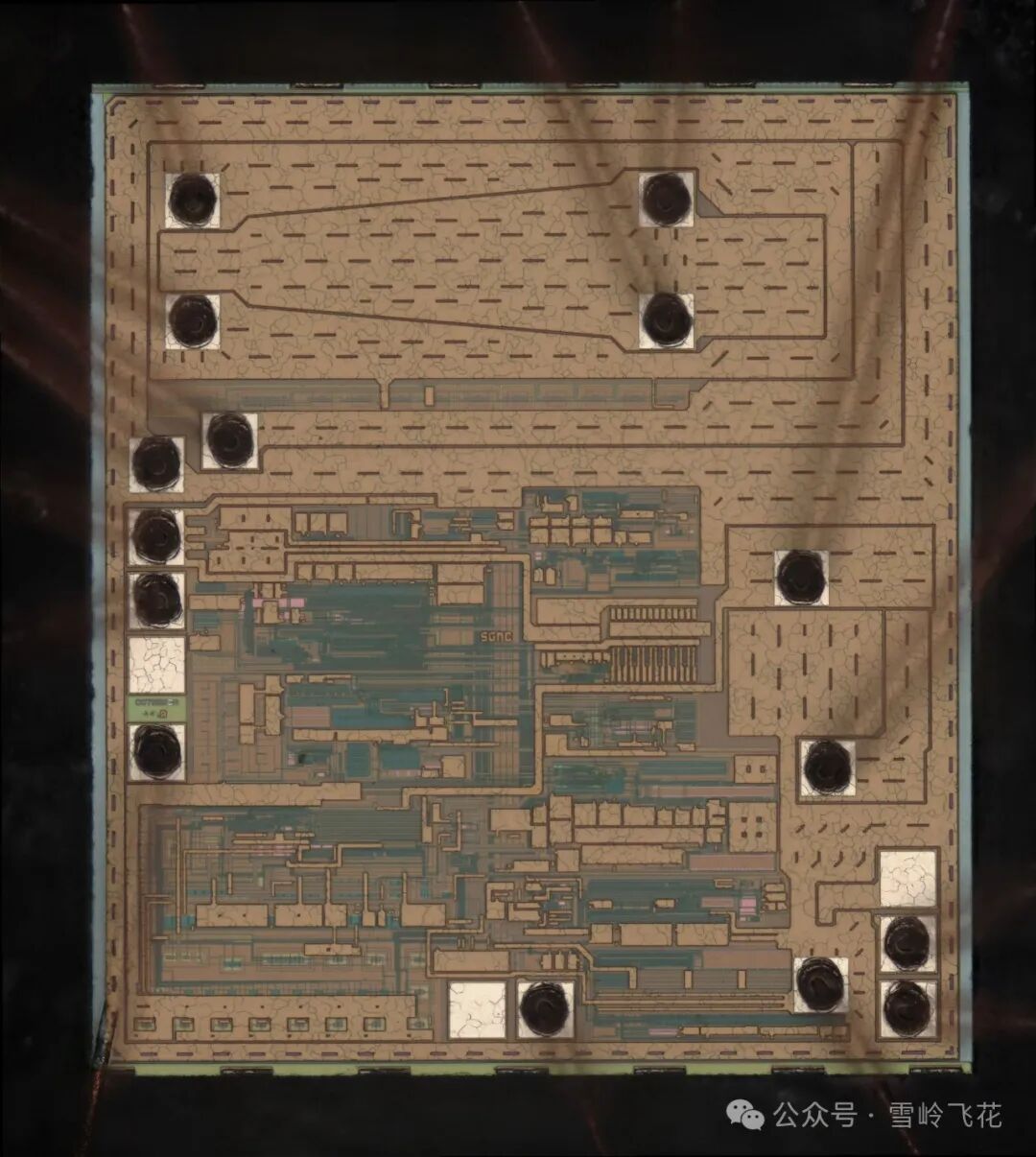
1) Chip #7
This is a QFN16 packaged chip, which should be a DCDC:
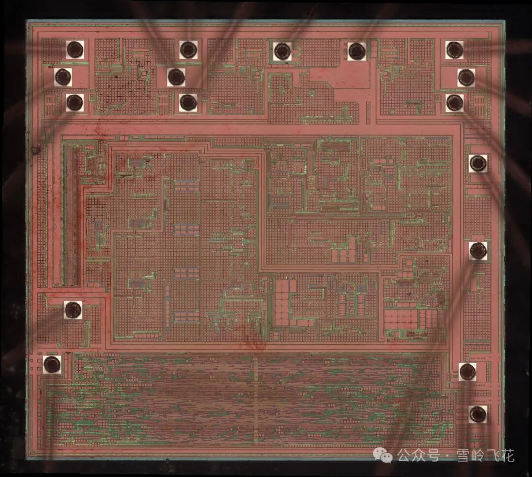
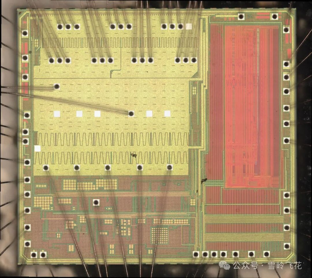
2) Chip #8
This is a QFN32 packaged chip, containing analog and logic circuits.
3) Chip #10
This is another DCDC:
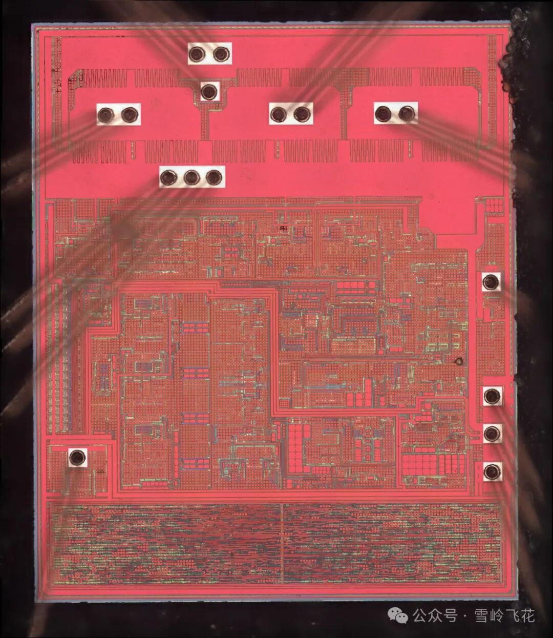
2. Chip #9
This is a logic chip, speculated to assist in processing laser transmission and reception signals.
3. Chip #13
Also contains logic and analog circuits, speculated to be for driving and controlling a small motor for vertical rotation.
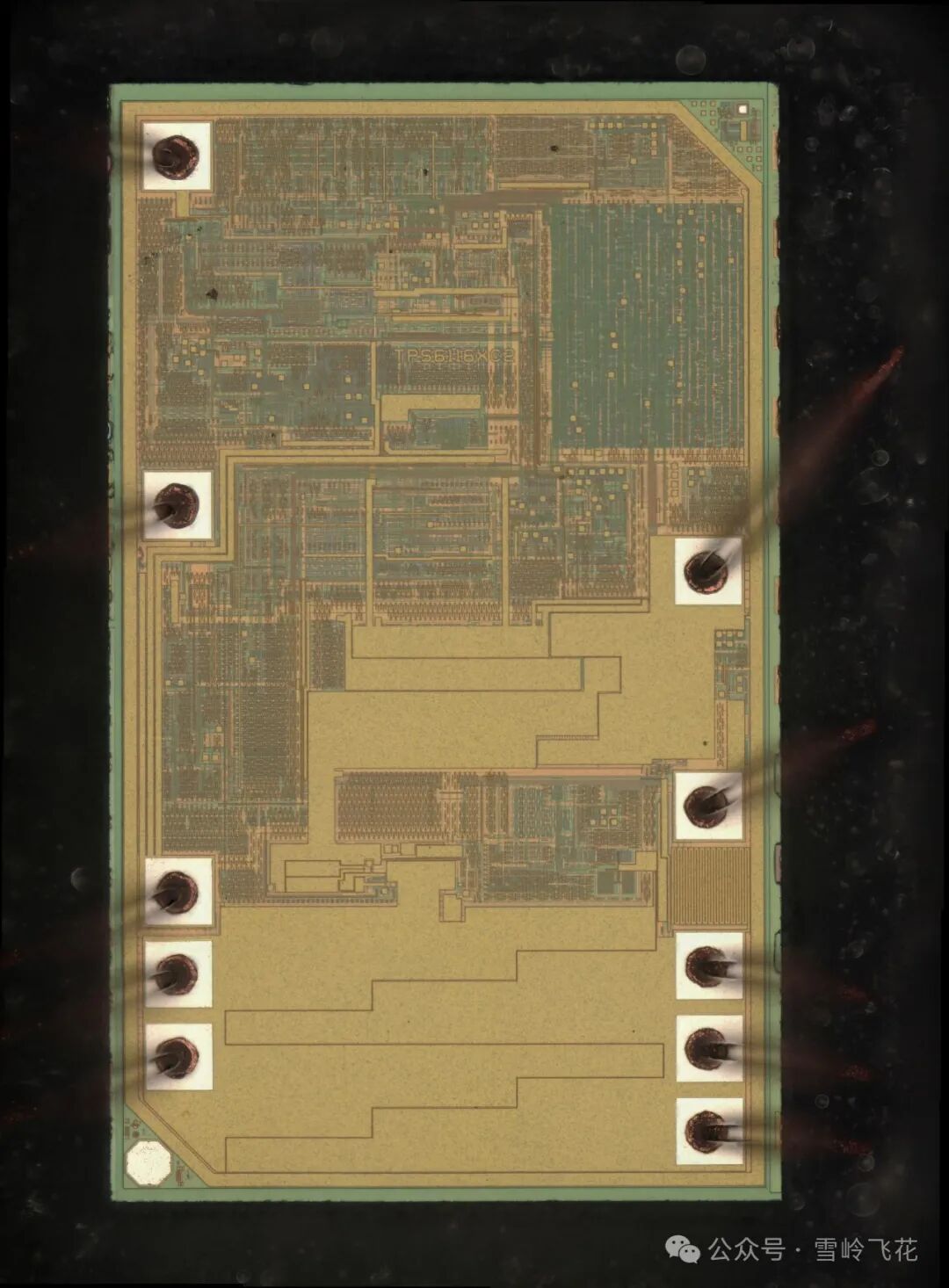
4. Chip #14
Chip #14 is the only chip with a visible model, which is “TPS6116xC2”. This is an LED Driver from TI, used for driving lasers.
Typical application diagram of TPS6116x:
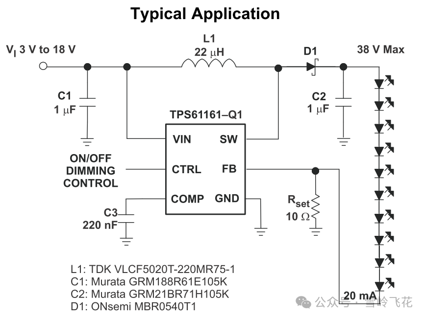
Image Source: TI
END
Feel free to leave comments and engage in discussions!


Industry Community