

1. What is QSPI?
The SPI protocol actually includes three types of protocol interfaces: Standard SPI, Dual SPI, and Queued SPI, corresponding to 3-wire, 4-wire, and 6-wire configurations respectively.
(1) Typically, when we refer to SPI, we mean Standard SPI, which has 4 signal lines: CLK, CS, MOSI, and MISO. The data line operates in full duplex.
(2) Dual SPI is specifically for SPI Flash and not for all SPI peripherals. For SPI Flash, full duplex is not commonly used, so the usage of MOSI and MISO is extended to operate in half duplex, effectively doubling the data transfer rate. In other words, for Dual SPI Flash, a command byte can be sent to enter dual mode, making MOSI become SIO0 (serial IO 0) and MISO become SIO1 (serial IO 1), allowing 2 bits of data to be transmitted in one clock cycle, thus doubling the data transfer.
(3) Similarly, it can be extended for SPI Flash, where Quad SPI Flash adds two more I/O lines (SIO2, SIO3) to transmit 4 bits of data in one clock cycle.
QSPI is short for Queued SPI.
2. Interface Issues
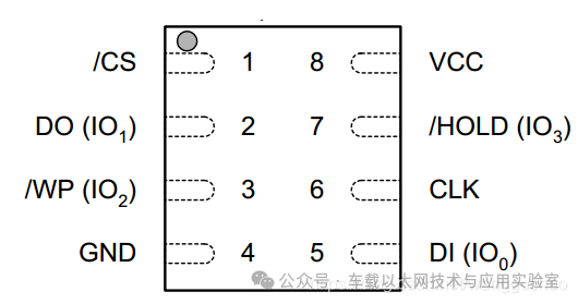
The above image is a schematic diagram of the pin interface of a certain SPI FLASH, which supports SPI communication, as well as DSPI or QSPI communication.
This chip has a total of 8 useful pins, with the function definitions of each pin as follows:
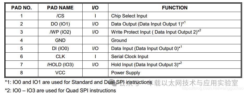
The detailed description of each pin is as follows:
1. Chip Select (/CS)
The Chip Select (/CS) signal is used to enable or disable the operation of the device. When CS is high, it indicates that the device is not selected, and the serial data output lines (DO or IO0, IO1, IO2, IO3) are in a high-impedance state. When CS is low, it indicates that the device is selected, allowing the FPGA to send data to or receive data from the QSPI Flash.
2. Serial Data Input Signal DI and Serial Output Signal DO
In the standard SPI protocol, data on the serial input signal DI is stored in the QSPI Flash on the rising edge of the serial clock signal (SCLK), and data from the QSPI Flash is serialized and output through the unidirectional DO pin on the falling edge of the serial clock signal (SCLK). In Dual SPI and Quad SPI, both DI and DO are bidirectional signals (they can act as both input and output).
3. Write Protect (/WP)
The Write Protect signal prevents erroneous data from being written to the status register of the QSPI Flash. The WP signal is active low, but when the QE bit of status register 2 is set to 1, the WP signal loses its write protection function and becomes a bidirectional data transmission signal for Quad SPI.
4. HOLD (/HOLD)
The HOLD signal is used to pause operations of the QSPI Flash. When the HOLD signal is low and CS is also low, the serial output signal DO will be in a high-impedance state, and the serial input signal DI and the serial clock signal SCLK will be ignored by the QSPI Flash. Once HOLD is pulled high, the read/write operations of the QSPI Flash can continue. When multiple SPI devices share the same SPI bus with the same signals, HOLD can be used to switch the direction of the signals. Similar to the WP signal, when the QE bit of status register 2 is set to 1, the HOLD signal loses its hold function and also becomes a bidirectional data transmission signal for Quad SPI.
5. Serial Clock Line
The serial clock line is used to provide the clock for serial input/output operations.
3. Usage of QSPI
3.1 Operating Modes
This interface can operate in the following three modes:
① Indirect Mode: All operations are executed using the QSPI registers.
② Status Polling Mode: Periodically read the external Flash status register, and an interrupt is generated when the flag is set to 1 (e.g., when erase or programming is complete).
③ Memory-Mapped Mode: The external Flash is mapped to the microcontroller’s address space, allowing the system to treat it as internal memory.
When using dual flash mode, two Quad-SPI Flash devices can be accessed simultaneously, effectively doubling throughput and capacity.
QSPI functional block diagram, dual flash mode disabled:
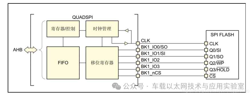
QSPI uses 6 signals to connect to Flash, which are four data lines BK1_IO0~BK1_IO3, one clock output CLK, and one chip select output (active low) BK1_nCS. Their functions are described as follows:
-
BK1_nCS: Chip select output (active low), suitable for FLASH 1. If QSPI always operates in dual flash mode, it can also be used for FLASH 2 device selection signal line. QSPI communication starts with the BK1_nCS line pulled low and ends with it pulled high.
-
CLK: Clock output, suitable for both memories, used for synchronizing communication data. It is generated by the communication host and determines the communication rate. Different devices support different maximum clock frequencies; for example, the maximum QSPI clock frequency for STM32 is fpclk/2, and the communication rate between two devices is limited by the slower device.
-
BK1_IO0: In dual/quad line mode, it is a bidirectional IO; in single line mode, it is a serial output, suitable for FLASH 1.
-
BK1_IO1: In dual/quad line mode, it is a bidirectional IO; in single line mode, it is a serial input, suitable for FLASH 1.
-
BK1_IO2: In quad line mode, it is a bidirectional IO, suitable for FLASH 1.
-
BK1_IO3: In quad line mode, it is a bidirectional IO, suitable for FLASH 1.
3.2 States
We can configure to choose which method to communicate with it. Before performing four-line read/write operations (QSPI), the QE (Quad Enable) bit in the register must be set to 1. Additionally, a four-line read operation requires waiting for 8 dummy clocks before reading data to speed up the reading process (for detailed information, please refer to the chip manual). Therefore, in addition to needing to add the state for four-line mode read/write data, a function to write the status register to enable the QE (Quad Enable) bit and a dummy wait for 8 clocks must also be added compared to single-line operations.
The states for four-line mode are as follows:
1. Idle State: Used to initialize the values of various registers.
2. Command Sending State: Used to send an 8-bit command code.
3. Address Sending State: Used to send a 24-bit address code.
4. Read Wait State (Single Line Mode): This state is entered when a read data operation is in progress, waiting for the data to be read.
5. Write Data State (Single Line Mode): In this state, the FPGA writes data into the QSPI Flash.
6. Write Status Register State: Used to set the QE (Quad Enable) bit in the status register to 1.
7. Dummy Clock State: Before reading data in four-line mode, it is necessary to wait for 8 dummy clocks.
8. Write Data State (Four Line Mode): In this state, the FPGA writes data into the QSPI Flash using four-line mode.
9. Read Wait State (Four Line Mode): In this state, it waits for the FPGA to complete reading data from the QSPI Flash using four-line mode.
10. End State: Indicates the end of an instruction operation and provides an end flag.
States 6-9 are additional states for four-line mode based on the single-line mode code.
3.3 Command Sequence
QSPI communicates with Flash through commands, where each command consists of five stages: instruction, address, alternate (multiplexed) bytes, dummy instruction, and data. Any stage can be skipped, but at least one of the instruction, address, alternate byte, or data stages must be included. nCS goes low before each command starts and goes high again after each command is completed. The timing of the read command in QSPI four-line mode is shown in the following diagram.
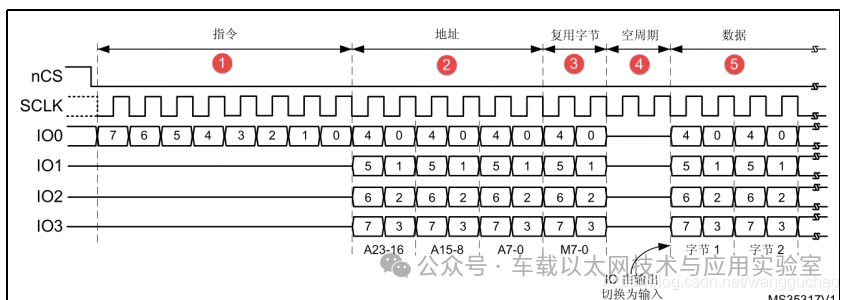
1) Instruction Stage
In this stage, an 8-bit instruction configured in the QSPI_CCR[7:0] register is sent to Flash, specifying the type of operation to be executed.
Although most Flash devices can only receive instructions one bit at a time through IO0/SO signal (single-line SPI mode), the instruction stage can choose to send 2 bits at once (in dual-line SPI mode through IO0/IO1) or 4 bits at once (in quad-line SPI mode through IO0/IO1/IO2/IO3). This can be configured through the IMODE[1:0] field in the QSPI_CCR[9:8] register. If IMODE = 00, the instruction stage is skipped, and the command sequence starts from the address stage (if present).
2) Address Stage
In the address stage, 1-4 bytes are sent to Flash, indicating the operation address. The number of address bytes to be sent is configured in the ADSIZE[1:0] field of the QSPI_CCR[13:12] register. In indirect mode and automatic polling mode, the address bytes to be sent are specified in the QSPI_AR register’s ADDRESS[31:0]; in memory-mapped mode, the address is given directly via AHB (from the core or DMA). The address stage can send 1 bit (in single-line SPI mode through SO), 2 bits (in dual-line SPI mode through IO0/IO1), or 4 bits (in quad-line SPI mode through IO0/IO1/IO2/IO3). This can be configured through the ADMODE[1:0] field in the QUADSPI_CCR[11:10] register. If ADMODE = 00, the address stage is skipped, and the command sequence directly proceeds to the next stage (if present).
3) Alternate Byte Stage
In the alternate byte stage, 1-4 bytes are sent to Flash, generally used to control the operation mode. The number of alternate bytes to be sent is configured in the ABSIZE[1:0] field of the QSPI_CCR[17:16] register. The bytes to be sent are specified in the QSPI_ABR register.
The alternate byte stage can send 1 bit (in single-line SPI mode through SO), 2 bits (in dual-line SPI mode through IO0/IO1), or 4 bits (in quad-line SPI mode through IO0/IO1/IO2/IO3). This can be configured through the ABMODE[1:0] field in the QSPI_CCR[15:14] register. If ABMODE = 00, the alternate byte stage is skipped, and the command sequence directly proceeds to the next stage (if present). There are cases where only a half-byte needs to be sent instead of a full byte during the alternate byte stage, such as when using dual-line mode and sending alternate bytes in two cycles. In this case, the firmware can use quad-line mode (ABMODE = 11) and send a byte, where the high 2 bits of ALTERNATE are set to “1” (IO3 remains high) and the low 2 bits are set to “0” (IO2 remains low). At this point, the high 2 bits of the half-byte are stored in bits 4:3 of ALTERNATE, and the low 2 bits are stored in bits 1 and 0. For example, if half-byte 2 (0010) is sent through IO0/IO1, ALTERNATE should be set to 0x8A (1000_1010).
4) Dummy Instruction Cycle Stage
In the dummy instruction cycle stage, no data is sent or received for a specified number of cycles (1-31), allowing time for the Flash to prepare data when using higher clock frequencies. The number of cycles specified in this stage is indicated in the DCYC[4:0] field of the QSPI_CCR[22:18] register. In SDR and DDR modes, the duration is specified as a certain number of full clock cycles. If DCYC is zero, the dummy instruction cycle stage is skipped, and the command sequence directly proceeds to the data stage (if present). The operation mode of the dummy instruction cycle stage is determined by DMODE. To ensure sufficient “turnaround” time for the data signal to switch from output mode to input mode, at least one dummy instruction cycle must be specified when receiving data from Flash in dual-line and quad-line modes.
5) Data Stage
In the data stage, any number of bytes can be received from or sent to Flash. In indirect mode and automatic polling mode, the number of bytes to be sent/received is specified in the QSPI_DLR register. In indirect write mode, the data sent to Flash must be written to the QSPI_DR register. In indirect read mode, the data received from Flash is obtained by reading the QSPI_DR register. In memory-mapped mode, the read data is sent back to Cortex or DMA directly via AHB. The data stage can send/receive 1 bit (in single-line SPI mode through SO), 2 bits (in dual-line SPI mode through IO0/IO1), or 4 bits (in quad-line SPI mode through IO0/IO1/IO2/IO3). This can be configured through the ABMODE[1:0] field in the QUADSPI_CCR[15:14] register. If DMODE = 00, the data stage is skipped, and the command sequence is completed immediately when nCS is pulled high. This configuration is only applicable for indirect write mode.

Disclaimer: We respect originality and emphasize sharing; the text and images are copyrighted by the original authors. The purpose of reprinting is to share more information and does not represent the position of this account. If your rights are infringed, please contact us promptly, and we will delete it as soon as possible. Thank you!
Original link:
https://blog.csdn.net/wangguchao/article/details/105593303