 Diamond: The Ultimate Material for Semiconductors
Since 2000, China has become the world’s largest producer of synthetic diamonds, with over 90% of the global production of diamond single crystals.
The chemical composition of diamond is carbon (C), which is a polymorph of the carbon element and is currently the hardest known natural material. Diamonds can be divided into natural diamonds and synthetic diamonds, with natural diamonds being a non-renewable resource that is scarce and expensive to mine; synthetic diamonds are mainly synthesized using two techniques: High-Temperature High-Pressure (HTHP) and Chemical Vapor Deposition (CVD).
In addition to traditional applications in industrial cutting and grinding materials, as well as decorative diamonds, diamond is also the ultimate material for semiconductors, possessing wide bandgap characteristics, high thermal conductivity, high electron mobility, high breakdown field strength, high thermal stability, and radiation resistance, which provide significant advantages in high-frequency and high-power devices.
Moreover, various countries have successively implemented related regulatory measures. As early as 2022, the United States first imposed an embargo on diamond for semiconductor use from China; Japan followed suit the same year, including semiconductor diamond design and manufacturing technology, diamond heteroepitaxial substrates, and other high-end diamond materials in export controls. In the second half of last year, China also decided to implement export controls on superhard diamond materials.
Beyond Silicon Carbide and Gallium Nitride, Diamond Empowers High-End Applications
Currently, third-generation compound semiconductor materials represented by silicon carbide and gallium nitride are widely used in high-voltage and high-current scenarios such as electric vehicles, rail vehicles, and 5G base stations. However, in certain specific high-power, high-frequency, high-temperature, high-radiation, ultraviolet detection, and high-precision sensor applications, the unique physical and chemical properties of diamond enable it to provide superior solutions.
Diamond is an excellent wide bandgap semiconductor material:
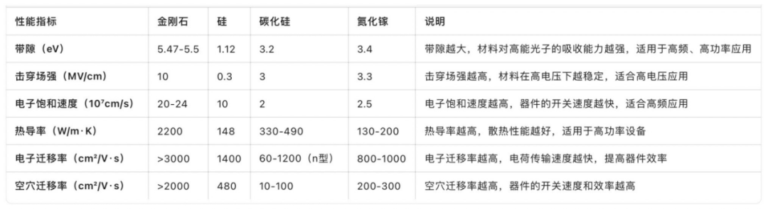
Comparison of key performance indicators of semiconductor materials: diamond, silicon, silicon carbide, and gallium nitride
Using diamond substrates, it is possible to develop high-temperature, high-frequency, high-power, radiation-resistant electronic devices, overcoming technical bottlenecks such as ‘self-heating’ and ‘avalanche breakdown’, particularly suited to the needs of applications in fields such as 5G communication, radar, aerospace, nuclear energy, optical communication, and optical detection.
The Industrialization Path of Diamond Semiconductors
Currently, the application of diamond in the semiconductor field is becoming a strategic high ground that major countries around the world are competing to layout. Experts predict that in the next 3-5 years, 4-inch diamond substrates are expected to achieve mass production.
-
Japan
Japan has laid out the entire industrial chain from diamond substrate research and development, device design, to equipment manufacturing, currently holding a leading position globally.
As early as 2021, Orbray in Tokyo developed mass production technology for 2-inch diamond wafers using heteroepitaxy and is expected to commercialize 4-inch wafers in the coming years.
In 2023, a team from Saga University in Japan successfully developed the world’s first power circuit using diamond semiconductors, focusing on space communication applications.
-
The United States
In 2023, the American startup Diamond Foundry created the world’s first single-crystal diamond wafer, with a diameter of 100 mm and weighing 110 carats.
In 2024, another startup, Diamond Quanta, announced significant breakthroughs in its proprietary new diamond semiconductor manufacturing and doping technology.
-
Europe
For example, the French company Diamfab aims to expand diamond wafer sizes to 4 inches by 2026. “Compared to traditional silicon-based semiconductors, diamond devices require a smaller wafer area and are less costly,” said Diamfab’s CEO, “Diamond devices are expected to compete with SiC on 4-inch wafers.”
-
China
China is also following closely, with a research team from Xi’an Jiaotong University achieving mass production of 2-inch heteroepitaxial single-crystal diamond self-supporting substrates in 2024, using microwave plasma chemical vapor deposition (MPCVD) technology. This project was awarded one of the top ten advancements in third-generation semiconductor technology in China for 2024.
Technical Challenges
Currently, the development of diamond electronic devices worldwide is limited by the constraints of large-size, high-quality single-crystal substrates.
In other words, the production equipment for large-size single-crystal diamonds and the preparation technology for high-quality single-crystal diamond substrates are key technologies that need to be overcome.
Specifically, the main technical challenges faced by semiconductor diamonds include:
-
Crystal Quality: The preparation of high-quality single-crystal diamond substrates is challenging, as defects in the crystal (such as dislocations, impurities, etc.) can affect the performance of semiconductor devices.
-
Size Limitations: Although methods like CVD can produce high-quality diamond films, the currently achievable substrate sizes are small, and the preparation of large-area, high-quality single-crystal diamond substrates still faces technical challenges.
-
Doping Technology: Achieving effective doping of diamond is one of the key technologies for its application in semiconductor devices. Currently, the doping technology for diamond is not mature enough; on one hand, it is difficult to precisely control doping concentration and uniformity; on the other hand, while boron doping can achieve n-type diamond, p-type doping remains a technical challenge, with no ideal doping elements or effective doping methods found, limiting the development of diamond-based bipolar devices.
-
Cost Issues: The preparation cost of diamond materials is relatively high, especially for high-quality single-crystal diamond substrates.
-
Processing Issues: Electronic devices have extremely high requirements for the surface flatness and dimensional accuracy of semiconductor materials. The high hardness of diamond significantly increases the difficulty of achieving such precision in processing, facing high costs and processing challenges in grinding, polishing, cutting, and shaping.
-
Compatibility with Existing Processes: The physical and chemical properties of diamond differ significantly from existing materials like silicon and silicon carbide, necessitating the development of new integration, packaging technologies, and processes.
While semiconductor diamonds possess many excellent physical and chemical properties, the numerous challenges they face need to be gradually overcome through continuous research and technological innovation.
At the same time, after China decided to implement export controls on gallium and germanium-related materials, for countries like the United States that rely on gallium nitride to develop the most advanced military radars, only breakthroughs in diamond semiconductors may hope to avoid China’s material advantages in the third-generation semiconductor field.