Siemens All Subjects + TIA Portal + EPLAN Electrical Drawing Video Recordings for Sale at Low Price!
Chuangkong Education Siemens All Subjects Course Introduction

1. What is MODBUS?
1. Basic Concept:
MODBUS is a soft communication protocol initially advocated by MODICON (now a brand of Schneider Electric). After practical applications by most companies, it has gradually been recognized and has become a standard communication protocol. As long as data communication or transmission follows this protocol, different systems can communicate. Currently, this protocol is widely used in RS232/RS485 communication processes.
There are two commonly used MODBUS communication protocols: one is MODBUS ASCII, and the other is MODBUS RTU. Generally, MODBUS ASCII is used for communication with a small amount of data and mainly text, while MODBUS RTU is used when the communication data volume is large and consists of binary values.
In practical applications, to solve a specific problem, people like to modify the MODBUS protocol to meet their needs (in fact, people often use their defined protocols for communication, which can solve problems but is not very standardized). A more common practice is to make minor modifications to the protocol while attaching the protocol format to the software manual or directly placing it in the help section, making it easier for users to communicate.
2. Brief Description of MODBUS Protocol:
The ACRXXXE series instruments use the MODBUS-RTU communication protocol. The MODBUS protocol defines the checksum, data sequence, etc., which are necessary for specific data exchange. The MODBUS protocol uses a master-slave response connection on a single communication line (half-duplex), meaning that signals are transmitted in opposite directions along a single communication line. First, the master computer’s signal addresses a unique terminal device (slave), and then the response signal from the terminal device is transmitted back to the master in the opposite direction.
The MODBUS protocol only allows communication between the master (PC, PLC, etc.) and the terminal device, and does not allow data exchange between independent terminal devices, so that each terminal device does not occupy the communication line during initialization and only responds to queries addressed to it.
3. Query-Response Cycle:
Query
The function code in the query message tells the selected slave device what function to execute. The data segment contains any additional information that the slave device needs to perform the function. For example, function code 03 requests the slave device to read holding registers and return their content. The data segment must contain the information to tell the slave device: from which register to start reading and how many registers to read. The error detection field provides a way for the slave device to verify whether the message content is correct.
Response
If the slave device generates a normal response, the function code in the response message is the same as the function code in the query message. The data segment includes the data collected by the slave device, such as register values or statuses. If an error occurs, the function code will be modified to indicate that the response message is erroneous, and the data segment will contain a code describing the error information. The error detection field allows the master device to confirm whether the message content is usable.
4. Transmission Method:
The transmission method refers to a series of independent data structures within a data frame and the finite rules used for data transmission. Below defines a transmission method compatible with the MODBUS protocol – RTU method.
Each byte’s bits:
· 1 start bit
· 8 data bits, with the least significant bit sent first
· No parity bit
· 1 stop bit
Error checking: CRC (Cyclic Redundancy Check)
5. Protocol
When a data frame reaches the terminal device, it enters the addressed device through a simple “port”. The device removes the “envelope” (data header) of the data frame, reads the data, and if there are no errors, it performs the requested task. Then, it adds its generated data back to the obtained “envelope” and returns the data frame to the sender. The returned response data contains the following content: slave address, executed command, requested data generated by executing the command, and a checksum. Any errors will not result in a successful response or will return an error indication frame.
6. Data Frame Format
|
Address |
Function |
Data |
Check |
|
8-Bits |
8-Bits |
N x 8-Bits |
16-Bits |
7. Address (Address) Field
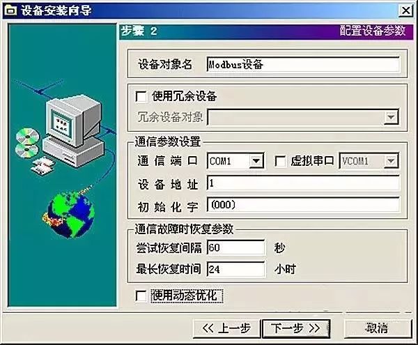
The address field is at the beginning of the frame, consisting of one byte (8-bit binary code), with a decimal range of 0-255. In our system, only addresses 1-247 are used, with other addresses reserved. These bits indicate the address of the terminal device specified by the user, which will receive data from the connected master. Each terminal device’s address must be unique, and only the addressed terminal will respond to queries containing that address. When the terminal sends back a response, the slave address data in the response tells the master which terminal is communicating with it.
8. Function (Function) Field
The function field code tells the addressed terminal what function to execute. The table below lists the function codes used by this series of instruments, along with their meanings and functions.
|
Code |
Meaning |
Action |
|
03 |
Read Data Register |
Obtain the current binary value of one or more registers |
|
16 |
Preset Multiple Registers |
Set binary values to a series of multiple registers (not open to ACRXXXE) |
9. Data (Data) Field
The data field contains the data required for the terminal to execute a specific function or the data collected when the terminal responds to a query. The content of this data may be numerical values, reference addresses, or setting values. For example, the function field code tells the terminal to read a register, and the data field needs to specify which register to start from and how many data to read. The embedded addresses and data vary according to type and content between the slave devices.
10. Error Check (Check) Field
This field allows the master and terminal to check for errors during the transmission process. Sometimes, due to electrical noise and other interference, a set of data may change on the line when transmitted from one device to another. Error checking ensures that the master or terminal does not respond to data that has changed during transmission, thus improving the system’s safety and efficiency. Error checking uses a 16-bit cyclic redundancy method (CRC16).
11. Error Detection Methods
Error checking (CRC) occupies two bytes and contains a 16-bit binary value. The CRC value is calculated by the transmitting device and then added to the data frame. The receiving device recalculates the CRC value when receiving data and compares it with the value in the received CRC field. If these two values are not equal, an error has occurred.
During the CRC calculation, a 16-bit register is first preset to all 1s, then each byte of the data frame is continuously XORed with the current value of the register. Only the 8 bits of each byte participate in generating the CRC; the start and stop bits and any parity bits used do not affect the CRC. When generating the CRC, each byte’s 8 bits are XORed with the content of the register, then the result is shifted to the low position, with the high position filled with “0”. The lowest bit (LSB) is shifted out and checked; if it is 1, the register will XOR with a preset fixed value (0A001H); if the lowest bit is 0, no action is taken.
The above processing is repeated until 8 shift operations are completed. After the last bit (the 8th bit) is shifted out, the next 8-bit byte is XORed with the current value of the register, and the same 8 shift XOR operations are performed. When all bytes in the data frame have been processed, the final value generated is the CRC value.
12. The process of generating a CRC is as follows:
1. Pre-set a 16-bit register to 0FFFFH (all 1s), called the CRC register.
2. XOR the 8 bits of the first byte in the data frame with the low byte of the CRC register, and store the result back in the CRC register.
3. Shift the CRC register to the right by one bit.
4. If the shifted-out bit is 1: XOR the CRC register with a preset fixed value (0A001H); if the shifted-out bit is 0: return to step 3.
5. Repeat steps 3 and 4 until 8 shifts are completed. Thus, one complete byte is processed.
6. Repeat steps 2 to 5 to process the next byte until all bytes have been processed.
7. The final value of the CRC register is the CRC value.
Additionally, there is a method of calculating CRC using a preset table, which is characterized by fast computation speed, but the table requires a large storage space. This method will not be elaborated here; please refer to relevant materials.
13. Detailed Communication Application Format
This section will use the format shown in the figure as much as possible (numbers are in hexadecimal).
|
Addr |
Fun |
Data start reg hi |
Data start reg lo |
Data #of regs hi |
Data #of regs lo |
CRC16 lo |
CRC16 hi |
|
01H |
03H |
00H |
00H |
00H |
03H |
05H |
CBH |
Addr: Slave Address
Fun: Function Code
Data start reg hi: Data Start Address High Byte
Data start reg lo: Data Start Address Low Byte
Data #of regs hi: Number of Data Registers High Byte
Data #of regs lo: Number of Data Registers Low Byte
CRC16 Hi: Cyclic Redundancy Check High Byte
CRC16 Lo: Cyclic Redundancy Check Low Byte
14. Read Data (Function Code 03)
l Query Data Frame
This function allows users to obtain data and system parameters collected and recorded by the device. There is no limit to the number of data requested by the master at one time, but it cannot exceed the defined address range.
The following example is to read 3 collected basic data (each address in the data frame occupies 2 bytes) UA, UB, UC from slave 01, where UA’s address is 0025H, UB’s address is 0026H, and UC’s address is 0027H.
|
Addr |
Fun |
Data start Addr hi |
Data start Addr lo |
Data#of regs hi |
Data #of regs lo |
CRC16 lo |
CRC16 hi |
|
01H |
03H |
00H |
25H |
00H |
03H |
14H |
00H |
l Response Data Frame
The response includes the slave address, function code, number of data, and CRC error check.
The following example is the response for reading UA, UB, UC (UA=082CH, UB=082AH, UC=082CH).
|
Addr |
Fun |
Byte count |
Data1 hi |
Data1 lo |
Data2 hi |
Data2 lo |
Data3 hi |
Data3 lo |
CRC16 lo |
CRC16 hi |
|
01H |
03H |
06H |
08H |
2CH |
08H |
2AH |
08H |
2CH |
94H |
4EH |
l Error Indication Code
If the address requested by the master does not exist, it will return an error indication code: FFH.
2. Features
Modbus has the following features:
1. Standard, open; users can use the Modbus protocol freely and safely without paying license fees or infringing intellectual property rights. Currently, there are over 400 manufacturers supporting Modbus, with over 600 products supporting Modbus.
2. Modbus can support multiple electrical interfaces, such as RS-232, RS-485, and can also be transmitted over various media, such as twisted pairs, fiber optics, wireless, etc.
3. The frame format of Modbus is simple, compact, and easy to understand. It is easy for users to use and simple for manufacturers to develop.
3. Function Code Definitions
1. ModBus Function Codes
|
01 |
READ COIL STATUS |
|
02 |
READ INPUT STATUS |
|
03 |
READ HOLDING REGISTER |
|
04 |
READ INPUT REGISTER |
|
05 |
WRITE SINGLE COIL |
|
06 |
WRITE SINGLE REGISTER |
|
15 |
WRITE MULTIPLE COIL |
|
16 |
WRITE MULTIPLE REGISTER |
4. Transmission Method
In the ModBus system, there are 2 transmission modes to choose from. These two transmission modes are equivalent to the ability of the slave PC to communicate. The choice should depend on the ModBus master used; each ModBus system can only use one mode, and mixing two modes is not allowed. One mode is ASCII (American Standard Information Exchange Code), and the other mode is RTU (Remote Terminal Unit).
Users can select the desired mode, including serial communication parameters (baud rate, parity method, etc.) when configuring each controller. All devices on a Modbus network must select the same transmission mode and serial port parameters. The selected ASCII or RTU method only applies to standard Modbus networks, defining each bit of the message segments transmitted continuously over these networks and determining how to package information into message fields and how to decode it. In other networks (like MAP and Modbus Plus), Modbus messages are converted into frames independent of serial transmission.
1. Transmission Mode Characteristics:
ASCII printable characters facilitate fault detection and are suitable for master computers and PCs programmed with high-level languages (such as Fortran). RTU is suitable for computers and PC hosts programmed in machine language.
Data transmitted in RTU mode are 8-bit binary characters. If converting to ASCII mode, each RTU character should first be divided into high and low parts, each containing 4 bits, then converted into hexadecimal equivalent values. The ASCII characters used to form messages are all hexadecimal characters. Although the characters used in ASCII mode are twice that of RTU mode, the decoding and processing of ASCII data are somewhat easier. Additionally, in RTU mode, message characters must be transmitted in a continuous data stream; in ASCII mode, there can be up to a 1-second interval between characters to accommodate slower machines.
The controller can be set to either of the two transmission modes (ASCII or RTU) in standard Modbus network communication.
2. ASCII Mode:
When the controller is set to communicate in ASCII mode on the Modbus network, each 8-bit byte of a message is transmitted as 2 ASCII characters. For example, the value 63H in ASCII mode needs to send two bytes, namely ASCII “6” (0110110) and ASCII “3” (0110011). The ASCII characters occupy either 7 or 8 bits, with the internationally used 7 bits being more common. The main advantage of this method is that the time interval for sending characters can reach 1 second without causing errors.
Code System
-
Hexadecimal, ASCII characters 0…9, A…F
-
Each ASCII character in the message consists of a hexadecimal character, with each byte’s bits
-
1 start bit
-
7 data bits, with the least significant bit sent first
-
1 parity bit; if no parity, there is no 1 stop bit (with parity), 2 bits (without parity) error detection field
-
LRC (Longitudinal Redundancy Check)
3. RTU Mode:
When the controller is set to communicate in RTU mode on the Modbus network, each 8-bit byte in the message is transmitted as its original value without processing. For example, 63H will be directly sent as 01100011 in RTU. The main advantage of this method is that there is no interval between data frame transmissions, resulting in a higher data density at the same baud rate compared to ASCII, allowing for faster transmission.
Code System
-
8-bit binary, hexadecimal numbers 0…9, A…F
-
Each 8-bit field in the message consists of one or two hexadecimal characters
-
Each byte’s bits: 1 start bit, 8 data bits, with the least significant bit sent first
-
1 parity bit; if no parity, there is no
-
1 stop bit (with parity), 2 bits (without parity)
5. Data Check Methods
1. CRC:
The CRC field consists of two bytes and contains a 16-bit binary value. It is calculated by the transmitting device and added to the message. The receiving device recalculates the received message’s CRC and compares it with the value in the received CRC field. If the two values are different, an error has occurred.
CRC is first loaded into a 16-bit register, all bits set to 1. Then a process is called to handle the continuous 8-bit bytes in the message with the current value in the register. Only the 8-bit data in each character is valid for the CRC; start bits, stop bits, and parity bits are invalid.
During the CRC generation process, each 8-bit character is XORed individually with the register content, and the result is shifted to the least significant bit, with the most significant bit filled with 0. The LSB is extracted and checked; if the LSB is 1, the register is XORed with a preset value; if the LSB is 0, no action is taken. This process is repeated until 8 shifts are completed. After the last bit (the 8th bit) is processed, the next 8-bit byte is XORed with the current value in the register. The final value generated is the CRC value after processing all bytes in the data frame.
When the CRC is added to the message, the low byte is added first, followed by the high byte.
The CRC-16 error check program is as follows: the message (here only involving data bits, not start bits, stop bits, and optional parity bits) is regarded as a continuous binary, with the most significant bit (MSB) sent first. The message is first multiplied by X^16 (left-shifted 16 bits), then divided by X^16 + X^15 + X^2 + 1. X^16 + X^15 + X^2 + 1 can be represented as the binary number 11000,0000,0000,0101. The integer quotient is ignored, and the 16-bit remainder is added to the message (MSB sent first), becoming 2 CRC check bytes. All 1s in the remainder are initialized to prevent all zeros from becoming a message received.
Devices accustomed to sending data in strings will preferentially send the most right bit of the character (LSB – least significant bit). In CRC generation, the first bit sent should be the most significant bit (MSB) of the dividend. Since no carry is used in the calculation, for ease of operation, the calculation of the CRC is set with the MSB on the right. The order of the polynomial must also be reversed to maintain consistency. The MSB of the polynomial is omitted, as it only affects the quotient and does not affect the remainder.
The steps to generate the CRC-16 check byte are as follows:
① Load a 16-bit register with all bits set to 1.
② XOR the high byte of this 16-bit register with the first 8-bit byte of the message. The result is placed in the 16-bit register.
③ Shift this 16-bit register to the right by one bit.
④ If the shifted-out bit is 1, XOR the generated polynomial with this register; if the shifted-out bit is 0, return to step ③.
⑤ Repeat steps ③ and ④ until 8 bits are shifted out.
⑥ XOR the next 8 bits with this 16-bit register.
⑦ Repeat steps ③ to ⑥ until all bytes in the message have been XORed with the 16-bit register and shifted 8 times.
⑧ The content of this 16-bit register is the 2-byte CRC error check, added to the message’s most significant bit. Additionally, in some non-ModBus communication protocols, CRC16 is often used as a check method, and several variants of CRC16 have been generated, using the CRC16 polynomial X^16 + X^15 + X^2 + 1, with the initial value of the 16-bit register set to 0000; using CRC16 in reverse order X^16 + X^14 + X^1 + 1, with the initial value of the register set to 0000 or FFFFH. The simple function of CRC is as follows:
2. LRC:
LRC error checking is used in ASCII mode. This error check is an 8-bit binary number that can be transmitted as 2 ASCII hexadecimal bytes. Convert the hexadecimal characters into binary, add them together without cyclic carry, and generate the LRC error check (see the figure). This LRC is verified by the receiving device and compared with the transmitted LRC, ignoring any colons, carriage return symbols (CR), line feed characters (LF), and any other non-ASCII hexadecimal characters during the operation.
Comparison of Modbus and PROFIBUS-DP Protocols
The content of the Modbus protocol is completely open, simple to implement, and can be easily realized by microcontrollers, PLCs, and DCS. In contrast, Profibus is more complex, requiring dedicated chips for secondary development and certification from higher organizations, which certainly raises development costs.
Of course, in terms of performance, serial-based Modbus RTU/ASCII communication cannot match PROFIBUS DP, but for simple instrument-level communication or small data volume communication at the controller level, Modbus is sufficient. In simple terms, Modbus is the *silk, while PROFIBUS is the wealthy and handsome!
Function Codes Supported by Modbus:
|
Function Code |
Name |
Function |
|
01 |
Read Coil Status |
Obtain the current status of a group of logical coils (ON/OFF) |
|
02 |
Read Input Status |
Obtain the current status of a group of switch inputs (ON/OFF) |
|
03 |
Read Holding Register |
Obtain the current binary value in one or more holding registers |
|
04 |
Read Input Register |
Obtain the current binary value in one or more input registers |
|
05 |
Write Single Coil |
Force a logical coil’s ON/OFF state |
|
06 |
Write Single Register |
Load a specific binary value into a holding register |
|
07 |
Read Exception Status |
Obtain the ON/OFF status of 8 internal coils, the addresses of which are determined by the controller |
|
08 |
Return Diagnostic Check |
Send a diagnostic check message to the slave for communication processing evaluation |
|
09 |
Programming (only for 484) |
Simulate the function of a programmer on the master to modify the PC slave logic |
|
10 |
Inquiry (only for 484) |
Enable the master to communicate with a slave performing a long program task, inquiring whether the slave has completed its operation task, only after sending a message with function code 9 can this function code be sent |
|
11 |
Read Event Count |
Enable the master to issue a single inquiry and immediately determine whether the operation was successful, especially when the command or other response generates a communication error |
|
12 |
Read Communication Event Record |
Enable the master to retrieve the communication event record of each slave’s ModBus transaction processing. If a transaction is completed, the record will provide information about errors |
|
13 |
Programming (184/384 484 584) |
Enable the master to simulate the function of a programmer to modify PC slave logic |
|
14 |
Inquiry (184/384 484 584) |
Enable the master to communicate with a slave performing a task, periodically inquiring whether the slave has completed its program operation, only after sending a message containing function 13 can this function code be sent |
|
15 |
Write Multiple Coils |
Force a series of consecutive logical coils’ ON/OFF state |
|
16 |
Write Multiple Registers |
Load specific binary values into a series of consecutive holding registers |
|
17 |
Report Slave Identification |
Enable the master to determine the type of the addressed slave and the status of its running indicator |
|
18 |
(884 and MICRO 84) |
Enable the master to simulate the function of a programmer to modify PC status logic |
|
19 |
Reset Communication Link |
After a non-modifiable error occurs, reset the slave to a known state, allowing the reset sequence byte |
|
20 |
Read General Parameters (584L) |
Display data information in the extended memory file |
|
21 |
Write General Parameters (584L) |
Write general parameters into the extended storage file or modify them |
|
22-64 |
Reserved for extended functions |
|
|
65-72 |
Reserved for user functions |
Reserved for user function expansion codes |
|
73-119 |
Illegal Function |
|
|
120-127 |
Reserved |
Reserved for internal use |
|
128-255 |
Reserved |
Used for abnormal response |
Detailed Explanation of Function Code Commands:
Among these function codes, the most frequently used ones are 1, 2, 3, 4, 5, and 6, which can achieve digital and analog read/write operations on the lower machine.
1. Command 01, Read Writable Digital Registers (Coil Status):
The computer sends the command: [Device Address] [Command Number 01] [Start Register Address High 8 Bits] [Low 8 Bits] [Number of Registers to Read High 8 Bits] [Low 8 Bits] [CRC Check Low] [CRC Check High]
Example: [11][01][00][13][00][25][CRC Low][CRC High]
Meaning as follows:
<1> Device Address: Multiple devices can be connected on a 485 bus; this device address indicates which device to communicate with. In the example, it intends to communicate with device 17 (decimal 17 is hexadecimal 11).
<2> Command Number 01: The command number for reading digital values is fixed at 01.
<3> Start Address High 8 Bits, Low 8 Bits: Indicates the starting address of the switch quantity to be read (the starting address is 0). For example, in the example, the starting address is 19.
<4> Register Count High 8 Bits, Low 8 Bits: Indicates how many switch quantities to read starting from the starting address. In the example, it is 37 switch quantities.
<5> CRC Check: Check from the beginning to this point. Device Response: [Device Address] [Command Number 01] [Returned Byte Count] [Data1] [Data2]…[Data n] [CRC Check High] [CRC Check Low]
Example: [11][01][05][CD][6B][B2][0E][1B] [CRC High] [CRC Low]
Meaning as follows:
<1> Device Address and Command Number are the same as above.
<2> Returned Byte Count: Indicates the number of bytes of data, which is the value of n in Data1, 2…n.
<3> Data1…n: Since each data is an 8-bit number, each data represents the value of 8 switch quantities, where each bit being 0 indicates that the corresponding switch is off, and 1 indicates that it is on. For example, in the example, it indicates that switch 20 (index number 19) is on, switch 21 is off, switch 22 is on, switch 23 is on, switch 24 is off, switch 25 is off, switch 26 is on, switch 27 is on… If the inquired switch quantity is not a multiple of 8, the high part of the last byte is meaningless and is set to 0.
<4> CRC Check is the same as above.
2. Command 05, Write Digital Quantity (Coil Status):
The computer sends the command: [Device Address] [Command Number 05] [Register Address to be Set High 8 Bits] [Low 8 Bits] [Data to be Set High 8 Bits] [Low 8 Bits] [CRC Check Low] [CRC Check High]
Example: [11][05][00][AC][FF][00][CRC High][CRC Low]
Meaning as follows:
<1> Device Address is the same as above.
<2> Command Number: The command number for writing digital values is fixed at 05.
<3> Register Address to be Set High 8 Bits, Low 8 Bits: Indicates the address of the switch to be set.
<4> Data to be Set High 8 Bits, Low 8 Bits: Indicates the state of the switch to be set. In the example, it indicates to close the switch. Note that it can only be [FF][00] to indicate on and [00][00] to indicate off; other values are illegal.
<5> Note that this command can only set the state of one switch quantity.
Device Response: If successfully set, the command sent by the computer is returned as is; otherwise, there is no response.
3. Command 03, Read Writable Analog Registers (Holding Registers):
The computer sends the command: [Device Address] [Command Number 03] [Start Register Address High 8 Bits] [Low 8 Bits] [Number of Registers High 8 Bits] [Low 8 Bits] [CRC Check High] [CRC Check Low]
Example: [11][03][00][6B][00][03] [CRC High][CRC Low]
Meaning as follows:
<1> Device Address is the same as above.
<2> Command Number: The command number for reading analog values is fixed at 03.
<3> Start Address High 8 Bits, Low 8 Bits: Indicates the starting address of the analog value to be read (the starting address is 0). For example, in the example, the starting address is 107.
<4> Register Count High 8 Bits, Low 8 Bits: Indicates how many analog values to read starting from the starting address. In the example, it is 3 analog values. Note that in the returned information, one analog value requires two bytes to be returned.
Device Response: [Device Address] [Command Number 03] [Returned Byte Count] [Data1][Data2]…[Data n] [CRC Check High][CRC Check Low]
Example: [11][03][06][02][2B][00][00][00][64][CRC High][CRC Low]
Meaning as follows:
<1> Device Address and Command Number are the same as above.
<2> Returned Byte Count: Indicates the number of bytes of data, which is the value of n in Data1, 2…n. In the example, 3 analog values are returned, as each analog value requires 2 bytes, totaling 6 bytes.
<3> Data1…n: Where [Data1][Data2] are the high and low bytes of the first analog value, [Data3][Data4] are the high and low bytes of the second analog value, and so on. In the example, the returned values are 555, 0, and 100.
<4> CRC Check is the same as above.
4. Command 06, Write Single Analog Register (Holding Register):
The computer sends the command: [Device Address] [Command Number 06] [Register Address to be Set High 8 Bits] [Low 8 Bits] [Data to be Set High 8 Bits] [Low 8 Bits] [CRC Check High] [CRC Check Low]
Example: [11][06][00][01][00][03] [CRC High][CRC Low]
Meaning as follows:
<1> Device Address is the same as above.
<2> Command Number: The command number for writing analog values is fixed at 06.
<3> Register Address to be Set High 8 Bits, Low 8 Bits: Indicates the address of the analog value register to be set.
<4> Data to be Set High 8 Bits, Low 8 Bits: Indicates the analog data to be set. For example, in the example, it sets the value of register 1 to 3.
<5> Note that this command can only set the state of one analog quantity.
Device Response: If successfully set, the command sent by the computer is returned as is; otherwise, there is no response.
5. Command 16, Write Multiple Analog Registers (Holding Registers):
The computer sends the command: [Device Address] [Command Number 16] [Register Address to be Set High 8 Bits] [Low 8 Bits] [Data Quantity High 8 Bits] [Data Quantity Low 8 Bits] [Data to be Set High 8 Bits] [Low 8 Bits][……][……] [CRC Check High] [CRC Check Low] 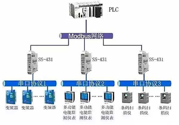
Example: [11][16][00][01][00][01][00][05] [CRC High][CRC Low]
Meaning as follows:
<1> Device Address is the same as above.
<2> Command Number: The command number for writing analog values is fixed at 16.
<3> Register Address to be Set High 8 Bits, Low 8 Bits: Indicates the address of the analog value register to be set.
<4> Data Quantity High 8 Bits, Low 8 Bits: Indicates the number of data to be set, which is 1 here.
<5> Data to be Set High 8 Bits, Low 8 Bits: Indicates the analog data to be set. For example, in the example, it sets the value of register 1 to 5.
Device Response: If successfully set, the command sent by the computer returns as follows; otherwise, there is no response. Device Response: [Device Address] [Command Number 16] [Register Address to be Set High 8 Bits] [Low 8 Bits] [Data Quantity High 8 Bits] [Data Quantity Low 8 Bits] [CRC Check High] [CRC Check Low], as in the example: [11][16][00][01][00][01] [CRC High][CRC Low]
(Content sourced from the internet; copyright belongs to the original author)
Disclaimer: If there are copyright issues, please contact for deletion! No person or organization shall bear relevant legal responsibilities.
Siemens All Subjects + TIA Portal + EPLAN Electrical Drawing Video Recordings for Sale at Low Price!
Chuangkong Education Siemens All Subjects Course Introduction
Schneider PLC training videos are available for free limited-time learning (not only can you learn for free, but there are also gifts, and passing the exam will earn a completion certificate)