
Click the blue text
Follow us
1. Introduction to SPI Protocol
The SPI protocol, proposed by Motorola, is a communication protocol (Serial Peripheral Interface) that allows chips to communicate with external devices in half/full duplex, synchronous, and serial modes. This interface can be configured as a master mode and provides a communication clock (SCK) for external slave devices. The interface can also operate in a multi-master configuration. It can be used for various purposes, including synchronous transmission using a single bidirectional data line, and reliable communication with CRC checks.
It is widely used in applications requiring high communication speeds between devices such as ADCs and LCDs and MCUs.
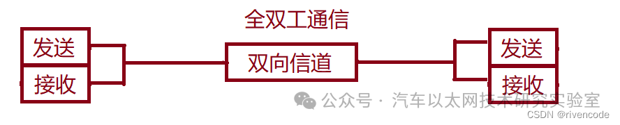
SPI generally adopts a bidirectional full-duplex communication method:
Full-duplex communication: At the same time, two devices can send and receive data simultaneously. In full-duplex mode, there is no need to switch directions, which requires both parties to have transmitters and receivers, and it needs 2 data lines.
2. SPI Physical Layer
Common connection methods between SPI communication devices:
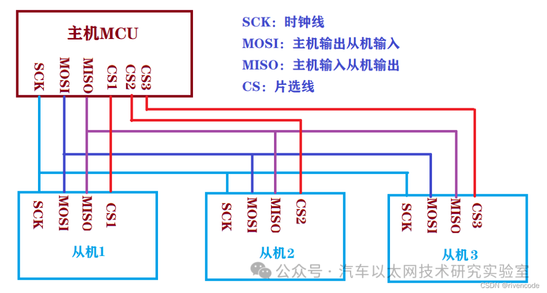
All signal lines of master or slave devices, SCK, MOSI, and MISO, are connected in parallel to the same SPI bus, using only these 3 buses;
-
CS Chip Select Signal Line
(Slave Select): The slave device selection signal line, also known as NSS or CS. When multiple SPI slave devices are connected to the SPI master, each slave device has its own independent NSS signal line, which occupies one pin of the master. Therefore, the number of slave devices corresponds to the number of chip select signal lines. When the master wants to select a slave device, it sets the NSS signal line of that slave device to low, and that slave device is selected. The master then begins SPI communication with the selected slave device, while other unselected slave devices (NSS pin high) will ignore data transmission on the bus.
SPI communication starts with the NSS line pulled low as a start signal and ends with the NSS line pulled high.
-
SCK Clock Signal Line
SCK (Serial Clock): The clock signal line used for synchronizing communication data. It can only be generated by the communication master and determines the communication speed. Different devices support different maximum clock frequencies. The maximum SPI clock frequency for STM32 is fpclk/2, and the communication speed between two devices is limited by the slower device.
-
MOSI Master Sends Slave Receives Data Line
MOSI (Master Output, Slave Input): The master device output/slave device input pin.
The master sends data to the slave, and the slave receives the data sent by the master.
-
MISO Master Receives Slave Sends Data Line
MISO (Master Input, Slave Output): The master device input/slave device output pin.
The slave sends data to the master, and the master receives the data sent by the slave.
3. SPI Protocol Layer
1. Start and Stop Signals of Communication
NSS is a signal line exclusive to each slave.
-
Start Signal: The NSS signal line changes from high to low. When the slave detects the start signal on its NSS line, the chip select is successful, and it begins to prepare for communication with the master.
-
Stop Signal: The NSS signal changes from low to high, which is the stop signal for SPI communication, indicating the end of this communication, and the selected state of the slave is canceled.
2. Data Validity
SPI uses the MOSI and MISO signal lines to transmit data, using the SCK signal line for data synchronization. The MOSI and MISO data lines transmit one bit of data during each clock cycle of SCK, and data input and output occur simultaneously. This means that when we send one data, we will also receive one data at the same time. There is no strict requirement on whether the MSB or LSB is sent first; it can be set, but the communication mode must be consistent. Generally, MSB first (most significant bit first) is used.
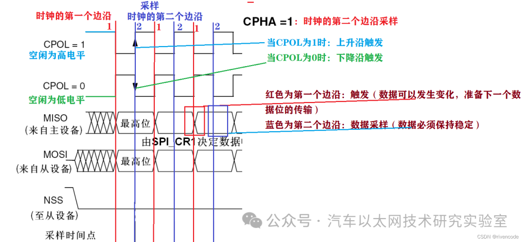
Like other protocols, SPI requires data to be stable during data acquisition. The triggering can allow data transmission level transitions to prepare for the next bit of data transmission, but the specific timing for data acquisition depends on the clock polarity (CPOL) and clock phase (CPHA) settings.
3. Clock Signal Phase and Polarity (Key Point)
The CPOL and CPHA bits of the SPI_CR register can combine to form four possible timing relationships.
-
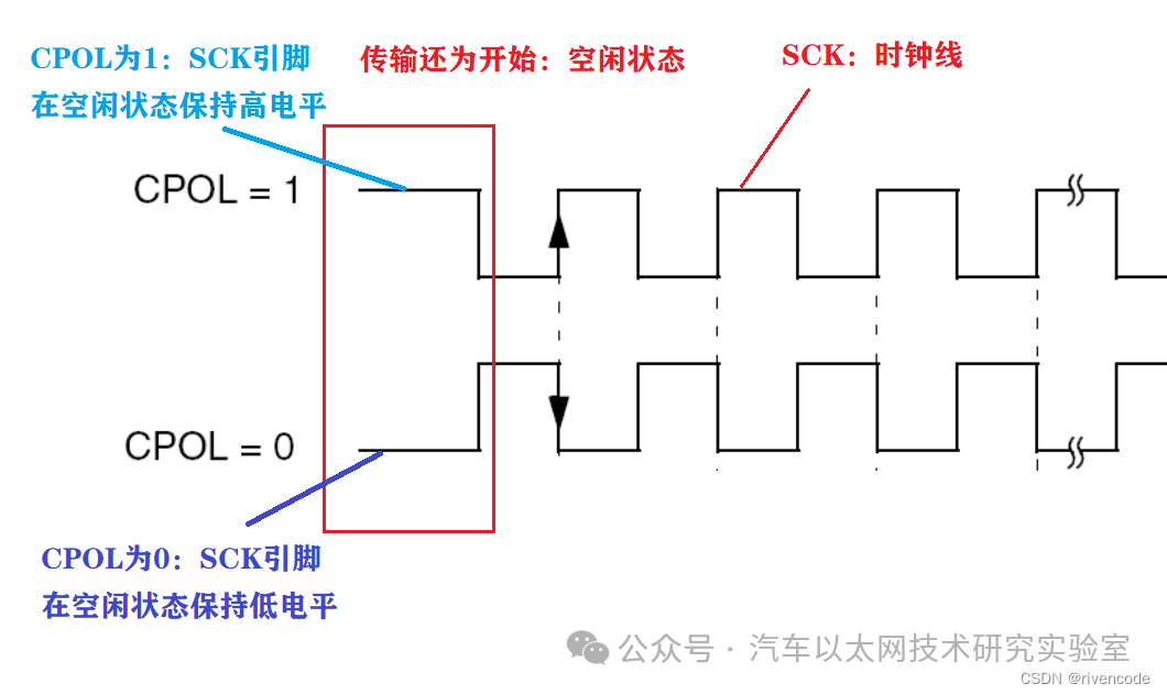
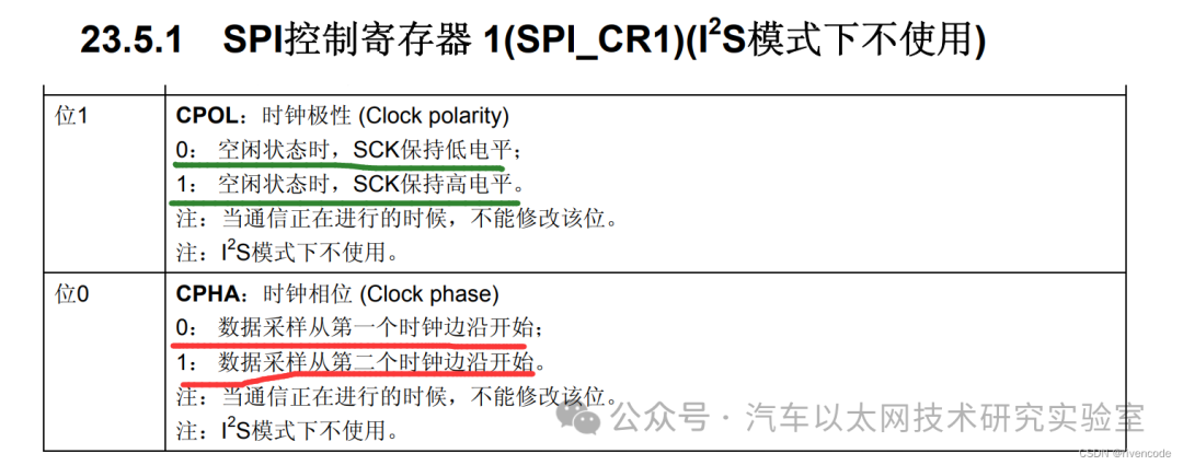
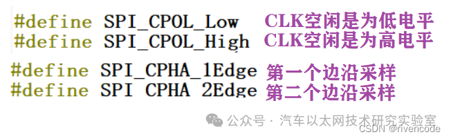
CPOL (Clock Polarity)
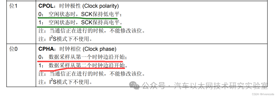
The CPOL (clock polarity) bit controls the idle state level of the clock when no data is being transmitted. This bit is effective for both master and slave modes.
If CPOL is cleared to ‘0’, the SCK pin remains low in the idle state;
If CPOL is set to ‘1’, the SCK pin remains high in the idle state.
-
CPHA (Clock Phase)
If the CPHA bit is set to ‘1’, data bits are sampled on the second edge of the SCK clock, and data is latched (held stable) on the second clock edge.
(If CPOL is ‘0’ at this time, it is sampled on the falling edge; if CPOL is ‘1’, it is sampled on the rising edge)
If the CPHA bit is cleared to ‘0’, data bits are sampled on the first edge of the SCK clock, and data is latched (held stable) on the first clock edge.
(If CPOL is ‘1’ at this time, it is sampled on the falling edge; if CPOL is ‘0’, it is sampled on the rising edge)
Therefore, it cannot be said that data is always sampled on the rising or falling edge; it depends on the values of CPOL and CPHA, which combine to yield four results.
-
When CPHA is ‘1’, if CPOL is ‘0’, it is sampled on the falling edge; if CPOL is ‘1’, it is sampled on the rising edge.
-
When CPHA is ‘0’, if CPOL is ‘1’, it is sampled on the falling edge; if CPOL is ‘0’, it is sampled on the rising edge.
Refer to the above diagram; however, when CPHA is ‘0’, it samples on the first edge of the clock.
-
CPOL and CPHA Register Configuration
Summary:
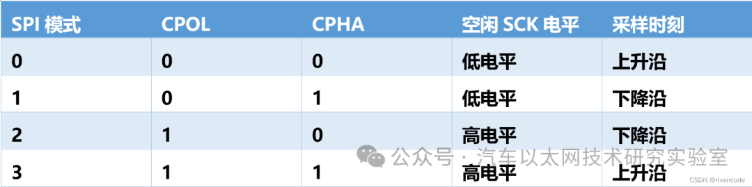
The specific mode to be used depends on which mode is supported by both communication parties. In this experiment, the FLASH communicating with the master supports modes 0 and 3, so we can randomly configure one.
4. SPI Characteristics and Architecture (Key Point)
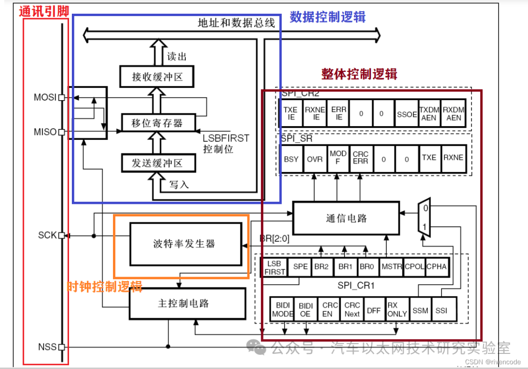
SPI Block Diagram:
1. Communication Pins
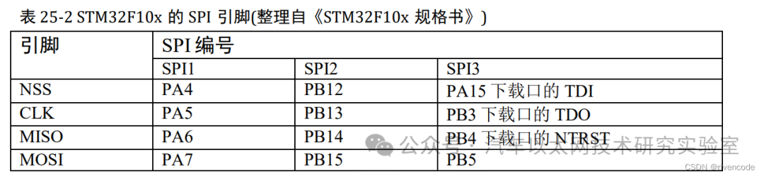
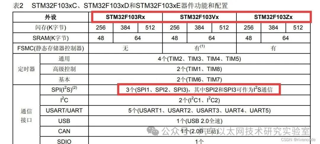
Different models of chips generally have 3 SPI peripherals, among which SPI2 and SPI3 support I2S communication because I2S is similar to the SPI protocol, so they share the same logic as shown in the above SPI block diagram.
2. Clock Control Logic
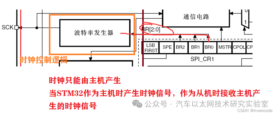
The clock signal of the SCK line is controlled by the baud rate generator based on the BR[0:2] bits in the “Control Register CR1”. This bit is the division factor for the fpclk clock, and the result of the division determines the output clock frequency on the SCK pin.
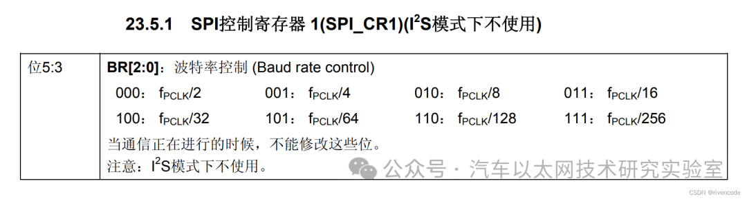
The SPI peripherals of STM32 can be used as both master and slave for communication, supporting a maximum SCK clock frequency of fpclk/2 (for STM32F103 chips, the default fpclk1 is 72MHz, and fpclk2 is 36MHz).
SPI1 mounted on the APB2 bus has a maximum communication rate of fpclk2/2 = 36Mbits/s.
SPI2 and SPI3 mounted on the APB1 bus have a maximum communication rate of pclk1/2 = 18Mbits/s.
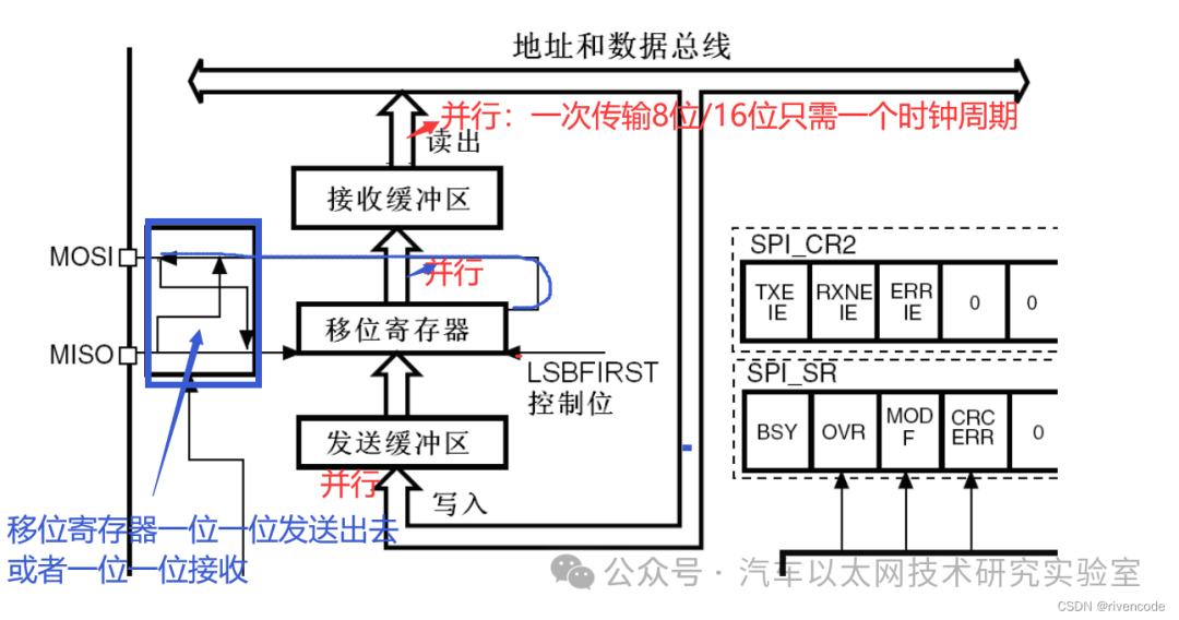
3. Data Control Logic (Very Important)
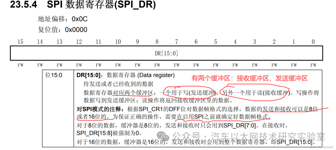
During reception, the received data is stored in an internal receive buffer;
During transmission, the data will first be stored in an internal transmit buffer before being sent.
Reading the SPI_DR register will return the contents of the receive buffer;
Writing data to the SPI_DR register will write to the transmit buffer.
Understanding the following diagram is very important:
Only the master sending data will generate a clock, so even if the master only receives data, we still need to send data to the slave, but the data sent by the master will be ignored by the slave.
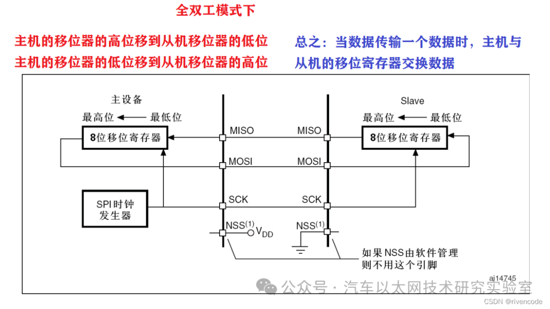
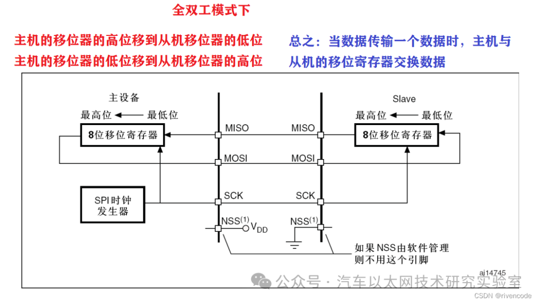
MOSI pins are connected to each other, and MISO pins are connected to each other. Thus, data is transmitted serially between the master and slave (with the MSB bit first). Communication is always initiated by the master device. The master sends data to the slave via the MOSI pin, and the slave returns data to the master via the MISO pin. This means that the data output and input in full-duplex communication are synchronized with the same clock signal, which is provided by the master device through the SCK pin.
Summary:
⦁ The serial shift register transmits bytes to the slave via the MOSI signal line, and the slave also returns the contents of its serial shift register to the master via the MISO signal line. Thus, the contents of the two shift registers are exchanged.
⦁ The write and read operations of peripherals are completed synchronously.
When the master sends one data to the slave, the master will also receive one byte (although this byte may be meaningless) because data transmission is equivalent to the exchange of data in the shift registers of both devices. Sending one data also means receiving one data simultaneously.
When the master receives data sent by the slave, since only the master sending data will generate a clock to drive the shift register, it must send an empty byte to the slave.
1. If only a write operation is performed, the master can simply ignore the received byte;
2. If the master wants to read a byte from the slave, it must send an empty byte to trigger the slave’s transmission, and of course, the slave will also ignore this data.
STM32 Master Mode Transmission Start
Focus on full-duplex mode:
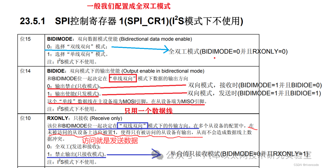
With all these fancy features, we generally use full-duplex mode; who would not want to utilize resources?
● Full-duplex mode (BIDIMODE=0 and RXONLY=0)
─ When data is written to the SPI_DR register (transmit buffer), transmission starts;
─ While transmitting the first bit of data, the data is simultaneously transferred in parallel from the transmit buffer to the 8-bit shift register (this demonstrates that parallel transmission only requires one clock cycle), and then it is serially shifted out to the MOSI pin in order;
─ At the same time, the data received on the MISO pin is serially shifted into the 8-bit shift register in order, and then it is transferred in parallel to the SPI_DR register (receive buffer).
● Unidirectional receive-only mode (BIDIMODE=0 and RXONLY=1)
─ When SPE=1, transmission starts;
─ Only the receiver is activated, and the data received on the MISO pin is serially shifted into the 8-bit shift register in order, and then it is transferred in parallel to the SPI_DR register (receive buffer).
● Bidirectional mode, sending (BIDIMODE=1 and BIDIOE=1)
─ When data is written to the SPI_DR register (transmit buffer), transmission starts;
─ While transmitting the first bit of data, the data is transferred in parallel from the transmit buffer to the 8-bit shift register, and then it is serially shifted out to the MOSI pin in order;
─ No data is received.
● Bidirectional mode, receiving (BIDIMODE=1 and BIDIOE=0)
─ When SPE=1 and BIDIOE=0, transmission starts;
─ The data received on the MOSI pin is serially shifted into the 8-bit shift register in order, and then it is transferred in parallel to the SPI_DR register (receive buffer).
─ The transmitter is not activated, and no data is serially sent to the MOSI pin.
4. Full-Duplex Sending and Receiving Process Mode (Super Important)
Preparation:
It is essential to understand the following diagram:
In summary: The master sends one byte of data while receiving one byte of data.
The second understanding of TXE and RXNE bits:
The data register SPI_DR corresponds to two buffers: the data transmit buffer and the data receive buffer.
-
Data Transmission
When data is transferred from the transmit buffer to the shift register, the TXE flag (transmit buffer empty) is set, indicating that the internal transmit buffer can receive the next data. If the TXEIE bit is set in the SPI_CR2 register, an interrupt will be generated at this time; writing to the SPI_DR register will clear the TXE bit.
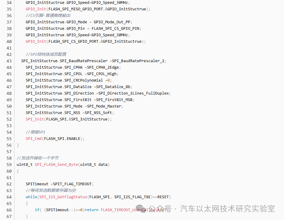
Note 1: Before writing to the transmit buffer, the software must confirm that the TXE flag is ‘1’; otherwise, new data will overwrite the data already in the transmit buffer.
Note 2: The data already in the transmit buffer will wait for the shift register to send the data bit by bit before being transferred to the shift register, meaning that the data in the shift register will not be overwritten.
-
Data Reception
At the last edge of the sampling clock, when data is transferred from the shift register to the receive buffer, the RXNE flag (receive buffer not empty) is set; it indicates that data is ready to be read from the SPI_DR register. If the RXNEIE bit is set in the SPI_CR2 register, an interrupt will be generated at this time; reading the SPI_DR register will clear the RXNE flag. In some configurations, the BSY flag can be used to wait for the end of data transmission when transmitting the last data.
-
Third understanding of the difference between serial and parallel
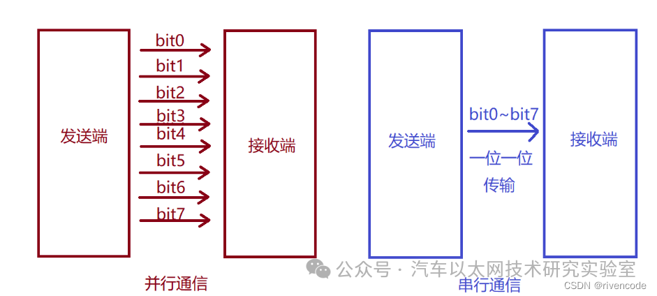
Data Transmission: Data is transferred in parallel from the transmit buffer to the shift register (parallel transmission only requires one clock cycle) and then serially shifted out to the MOSI pin (serial transmission of one bit requires one clock cycle).
Data Reception: The data received on the MISO pin is serially shifted into the 8-bit shift register in order, and then it is transferred in parallel to the SPI_DR register (receive buffer).
Summary: The transfer from the shift register to the buffer is parallel, while the data from the shift register to the pin is serial.
The key point is:
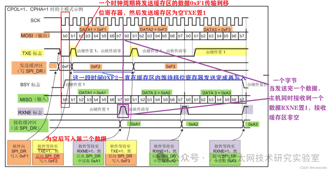
If you understand the previous content, this diagram should not be a problem.
5. SPI Initialization Structure
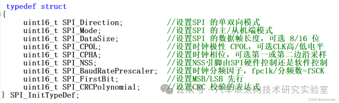
SPI_Direction
-
There is a detailed introduction above, so I won’t elaborate further.

-
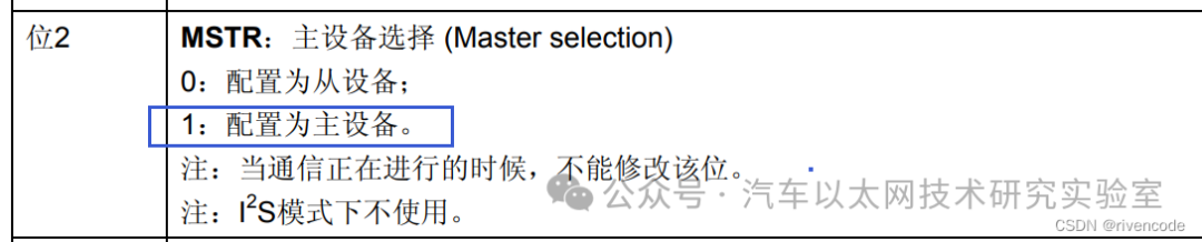
SPI_Mode
This member sets the SPI to operate in master mode (SPI_Mode_Master) or slave mode (SPI_Mode_Slave). The master generates the clock signal; if configured as a slave, the STM32 SPI peripheral will accept the external SCK signal.
-
SPI_DataSize
This member can choose the SPI communication data frame size to be 8 bits (SPI_DataSize_8b) or 16 bits (SPI_DataSize_16b).

-
SPI_CPOL and SPI_CPHA
-
SPI_NSS
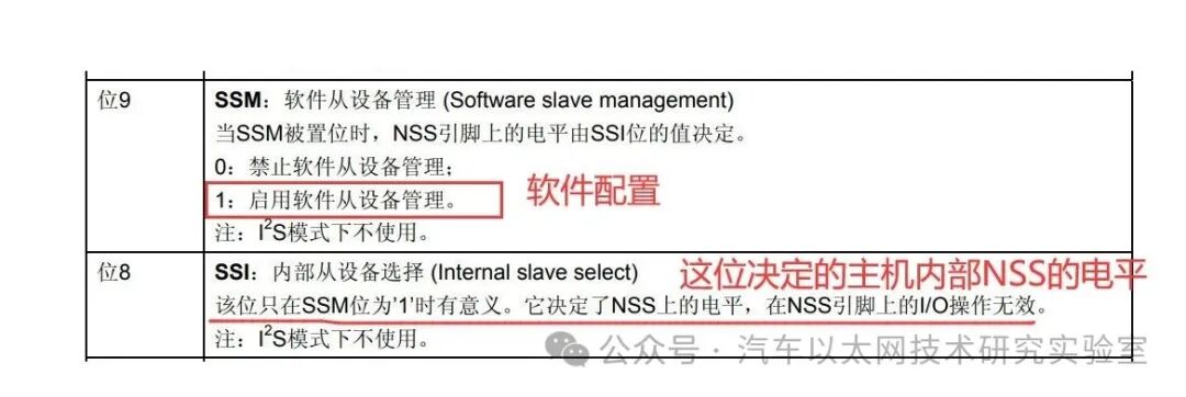
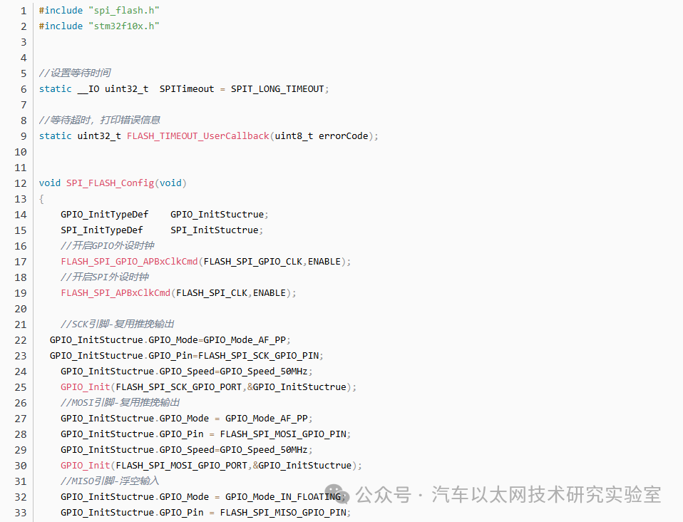
This member configures the usage mode of the NSS pin, which can be selected as hardware mode (SPI_NSS_Hard) or software mode (SPI_NSS_Soft). In hardware mode, the SPI chip select signal is automatically generated by the SPI hardware, while in software mode, we need to manually pull the corresponding GPIO port high or low to generate the deselect and select signals. In practice, software mode is more commonly used.
-
SPI_BaudRatePrescaler

-
SPI_FirstBit
The STM32 SPI module can be programmed to control this feature through this structure member.

-
SPI_CRCPolynomial
This is the polynomial used in the CRC check of SPI. If we use CRC checks, we will use the parameters (polynomial) of this member to calculate the CRC value. After configuring these structure members, we need to call the SPI_Init function to write these parameters into the registers to implement SPI initialization, and then call SPI_Cmd to enable the SPI peripheral.
The following is for understanding:
Status Flags:
The application can fully monitor the status of the SPI bus through three status flags.
Transmit Buffer Empty Flag (TXE)
This flag is ‘1’ when the transmit buffer is empty, indicating that the next data can be written into the buffer. The TXE flag is cleared when writing to SPI_DR.
Receive Buffer Not Empty (RXNE)
This flag is ‘1’ when there is valid received data in the receive buffer. Reading the SPI data register can clear this flag.
Busy Flag
The BSY flag is set and cleared by hardware (writing to this bit has no effect). This flag indicates the status of the SPI communication layer.
When it is set to ‘1’, it indicates that the SPI is busy with communication, but there is one exception: in the master mode bidirectional receive mode (MSTR=1, BDM=1, and BDOE=0), the BSY flag remains low during reception. Before the software closes the SPI module and enters sleep mode (or turns off the device clock), the BSY flag can be used to detect whether the transmission has ended, thus avoiding corruption of the last transmission. Therefore, it is necessary to strictly follow the process described below.
The BSY flag can also be used to avoid write conflicts in multi-master systems.
Except for the master mode bidirectional receive mode (MSTR=1, BDM=1, and BDOE=0), the BSY flag is set to ‘1’ when transmission starts.
This flag will be cleared to ‘0’ in the following situations:
● When the transmission ends (in master mode, if it is a continuous communication situation, there are exceptions);
● When the SPI module is turned off;
● When a master mode fault occurs (MODF=1).
If communication is not continuous, the BSY flag will be low between the transmission of each data item.
<spanwhen communication="" continuous:
● In master mode: The BSY flag remains high throughout the transmission;
● In slave mode: The BSY flag is low for one SPI clock cycle between each data item transmission.

Closing SPI
When communication ends, the SPI module can be turned off to terminate communication. Clearing the SPE bit will turn off SPI.
In some configurations, if the transmission has not been completed and the SPI module is turned off and enters sleep mode, it may lead to the current transmission being corrupted, and the BSY flag also becomes unreliable.
To avoid this situation, it is recommended to follow the steps below when closing the SPI module:
In full-duplex mode (BIDIMODE=0, RXONLY=0) in master or slave mode:
1. Wait for RXNE=1 and receive the last data;
2. Wait for TXE=1;
3. Wait for BSY=0;
4. Close SPI (SPE=0), and finally enter sleep mode (or turn off the clock of this module).
Overflow Error
When the master has sent a data byte, and the slave has not cleared the RXNE generated by the previous data byte, it results in an overflow error. When an overflow error occurs:
● The OVR bit is set to ‘1’; if the ERRIE bit is set, an interrupt will be generated.
At this time, the data in the receiver buffer is not the new data sent by the master; reading the SPI_DR register returns the previously unread data, and all subsequently transmitted data will be discarded.
Reading the SPI_DR register and the SPI_SR register in sequence can clear the OVR.
Summary: If an overflow error occurs, the data received afterward will be discarded, and reading the receive buffer will yield the original unread data.
This is also why we must receive one data when sending one data; for example, when we send a command to the flash, the first byte returned by the flash will only be an empty byte (should be 0xFF). At this time, RXNE is set, and if we do not read it, we will…
5. NorFLASH Chip – NM25Q64EV
Introduction to FLASH
FLASH memory, also known as flash memory, is a non-volatile memory that retains data after power loss, similar to EEPROM, but FLASH memory generally has a larger capacity than EEPROM and has largely replaced it. Common devices in our lives, such as USB drives, SD cards, SSDs, and the devices used in STM32 chips for program storage, are all types of FLASH memory. The main difference in storage control is that FLASH chips can only be erased in large blocks, while in the “I2C section,” we learned that EEPROM can be erased byte by byte.
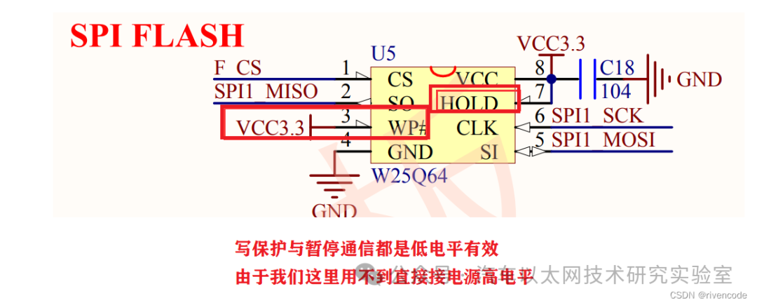
The NM25Q64EV chip is basically the same as the W25Q64BV, with only the device address being different.
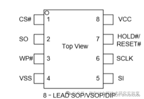
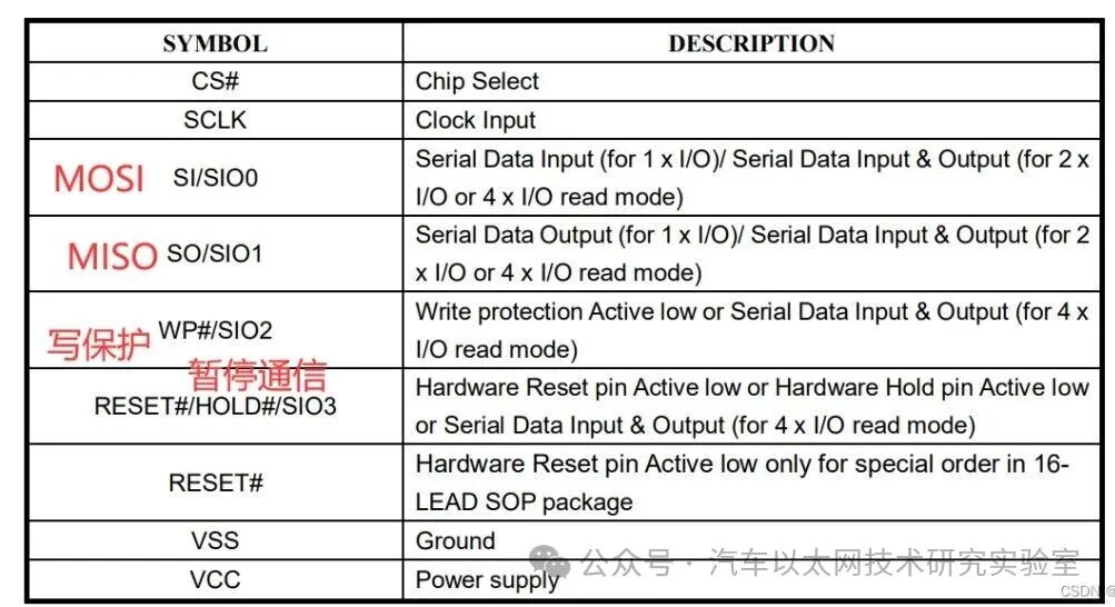
Schematic Diagram:
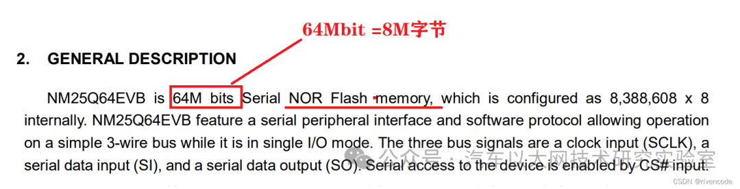
Hardware SPI Protocol Logic
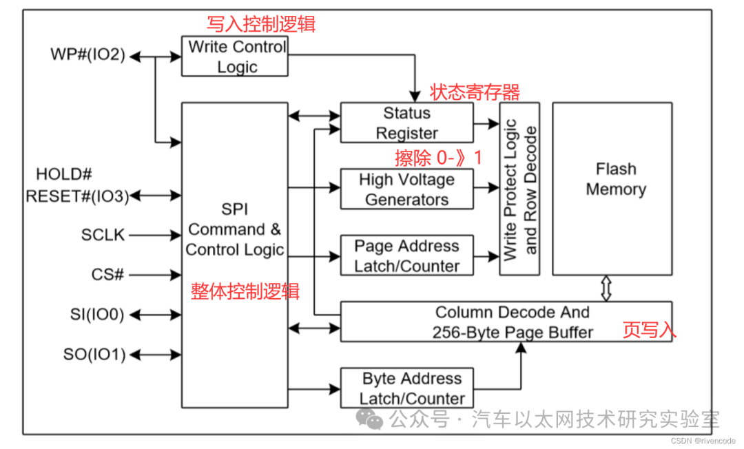
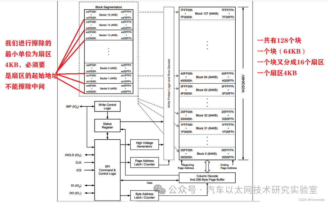
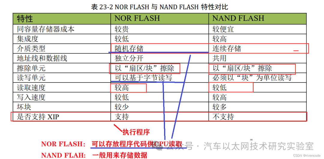
1. Storage Characteristics of NorFLASH (Key Point)
1. Data must be erased before writing.
2. During erasure, all bits of data are reset to 1.
3. When writing data, only bits that are 1 can be changed to 0 (this is why data must be erased before writing).
4. The minimum unit of erasure is a sector (4KB), which is erased to all 1s.
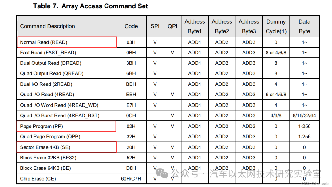
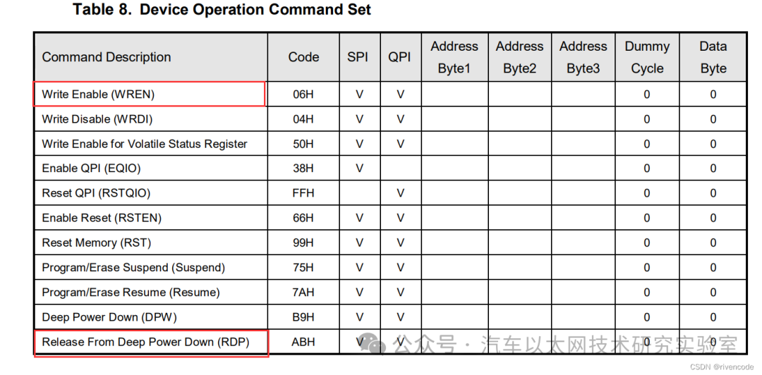
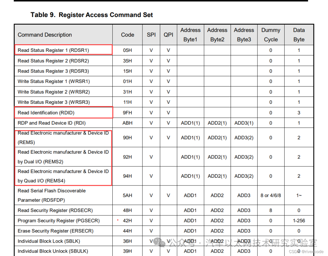
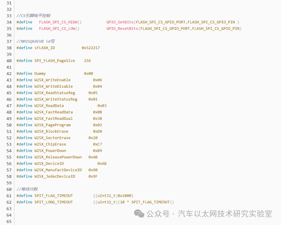
2. Summary of FLASH Instructions (Key Point)
The instructions marked in red are the commonly used ones.
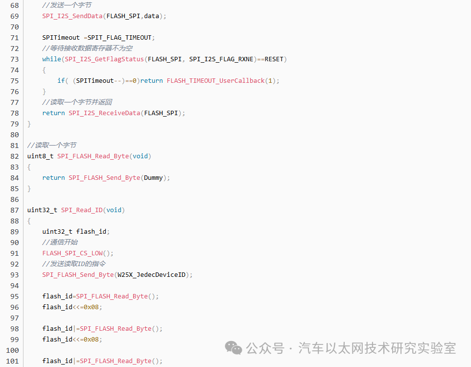
1) Read Device ID
-
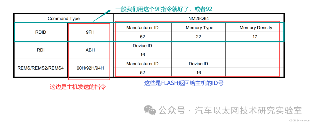
ABH Command
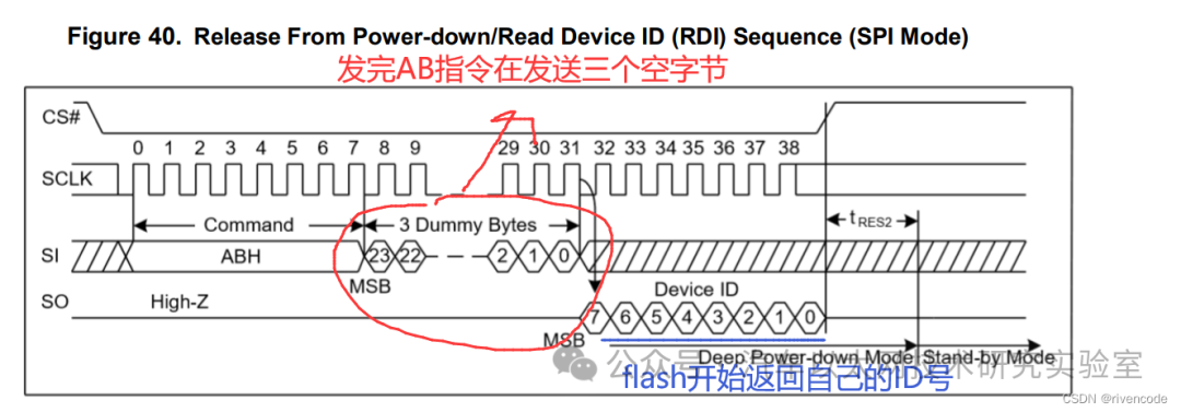
Returns 16H
-
9FH Command
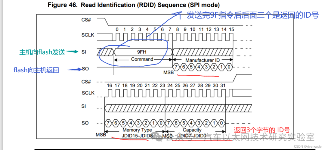
Returns 522217H
-
90H Command
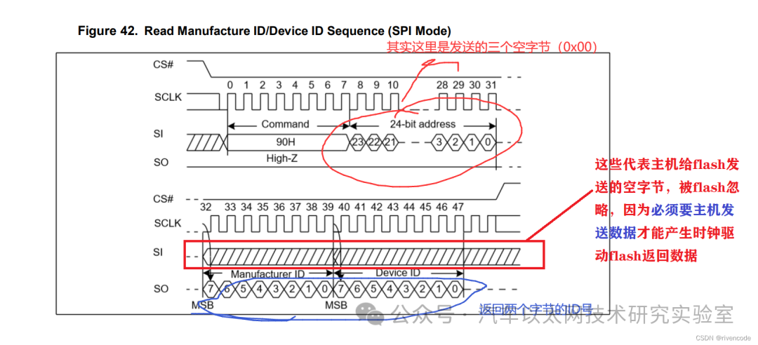
Returns 5216H
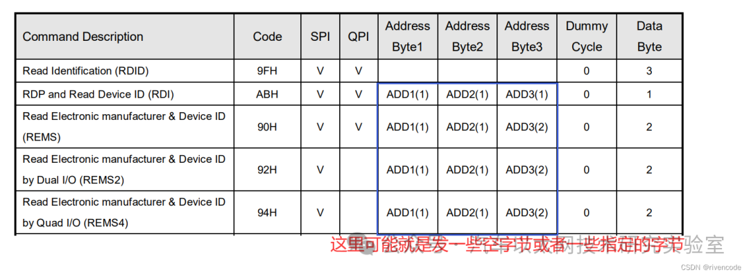
Note: When we receive the ID returned by the flash after sending the command, the master must also send an empty byte (0x00) to the flash because only the master sending data can generate a clock to drive the flash to return data to the master (here is the ID number).
Since sending and receiving share the same clock: the master sends an empty byte while receiving data sent by the slave (here is the ID number).
2) Read Status Register 1
Reading Status Register 1 determines whether the FLASH chip is busy (during data erasure or writing data).
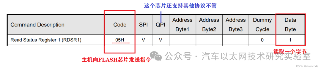
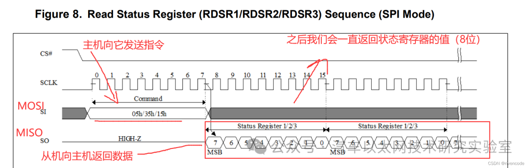
For command codes “05H”/”35H”/”15H”, the corresponding output status register bits are S7~S0 / S15-S8 / S16-S23.
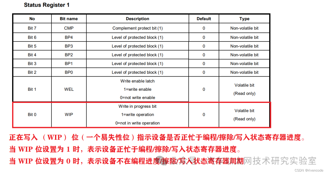
After receiving the data, we only need to check the first bit (WIP bit) to determine whether the FLASH chip is busy.
When we write data or the flash erases its own data, we must check whether the flash chip has completed writing or erasing.
3) Erase Sector

Why is it a 24-bit address? Because a 24-bit address is sufficient to represent 8M bytes.
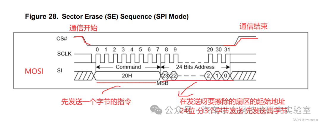
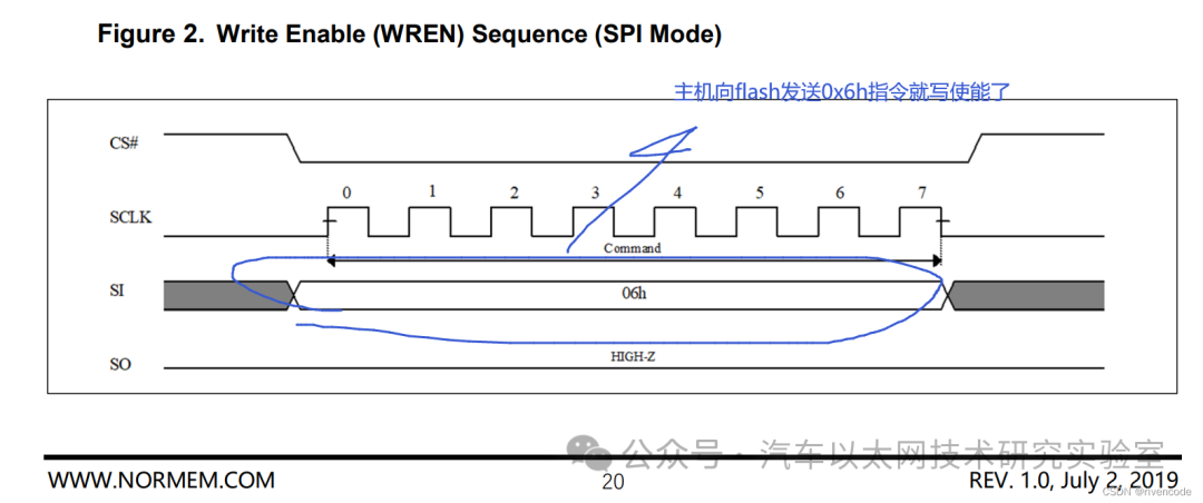
4) Write Enable
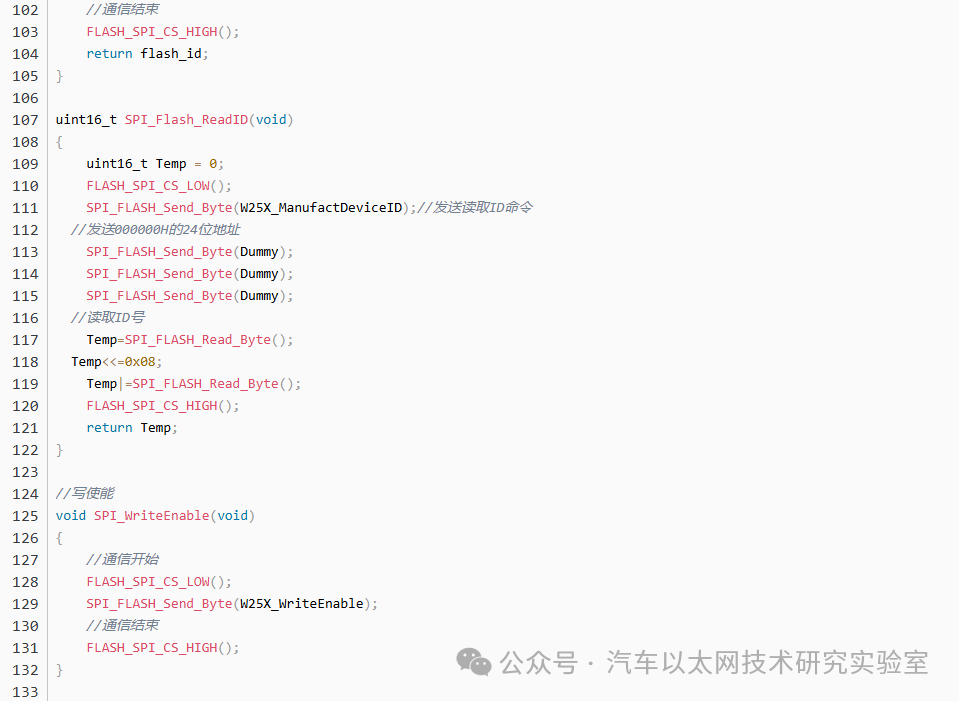
When writing data to the flash or erasing its own data, it is necessary to write enable first.
Erasing data in flash means changing all data to 1, which is equivalent to a write operation.
5) Page Write Data
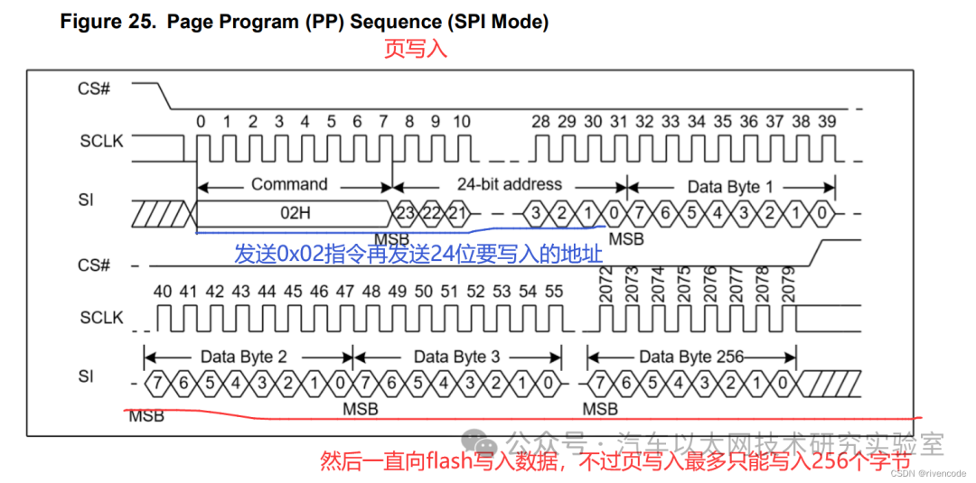
Page write characteristics:
1. The amount of data written at one time cannot exceed 256 bytes.
2. If more than 256 bytes are written, the subsequent bytes will not be written.
3. The address to be written should be aligned to 256 (Addr%256=0).
4. If the number of bytes written to an unaligned address exceeds 256, the excess part will fail to write.
6) Read Data
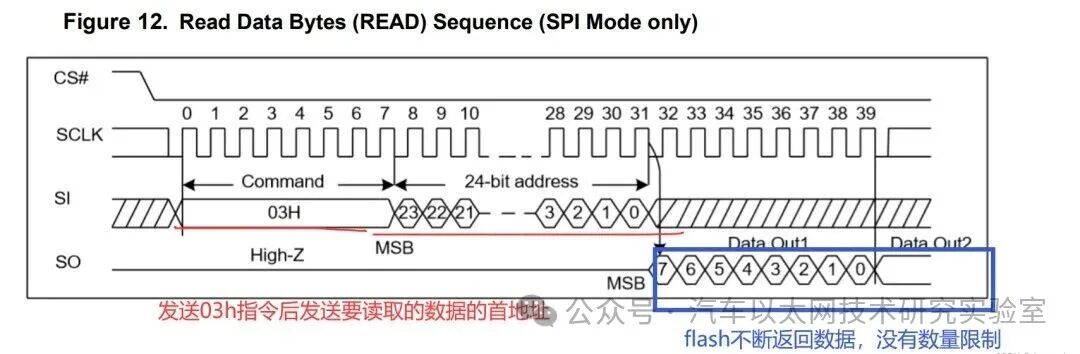
The address automatically increments to the next higher address after each address data byte is read out. Therefore, the entire memory can be read using a single read data byte command. When the highest address is reached, the address counter will roll back to 0.
Data can be read continuously as long as the clock keeps driving.
7) FLASH Low Power Mode and Wake-Up
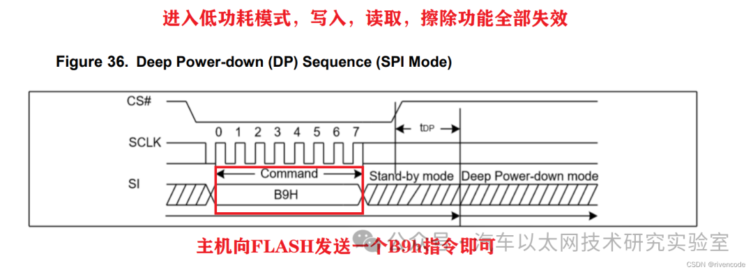
The enter deep power-down (DP) command puts the device in a deep sleep mode, and all write/program/erase commands will be ignored.
Release from Power-Down Mode
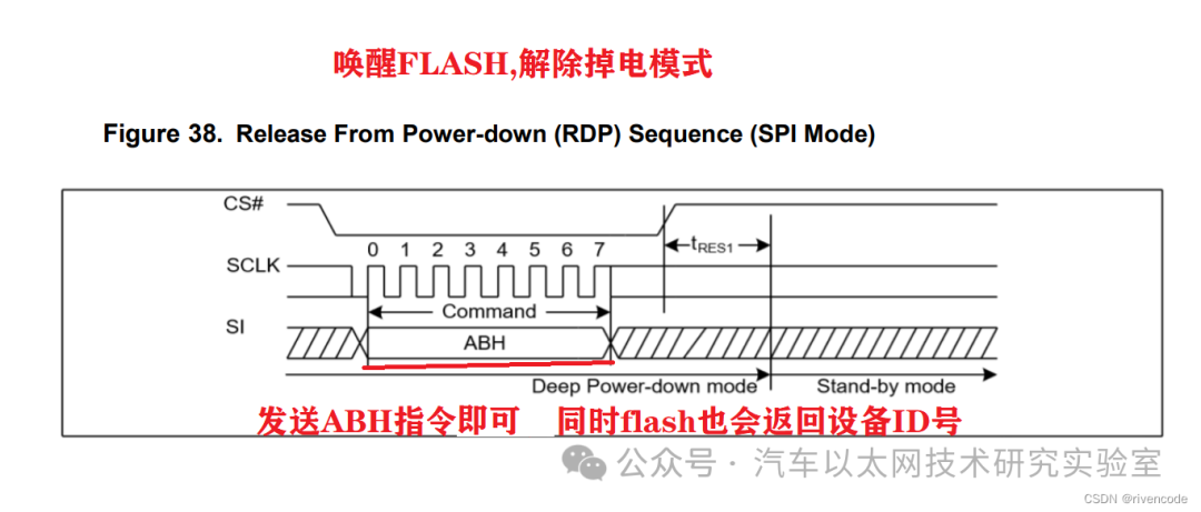
The release command from power-down (RDP) and read device ID (RDI) is a multipurpose command that can be used to release the device from shutdown or obtain the device’s electronic identification (ID) number.
When used solely to obtain the device ID without being in shutdown mode, this command is initiated by driving the CS# pin low, followed by sending the instruction code “ABH” and then 3 dummy bytes (empty bytes).
These are the commonly used commands; writing code according to this logic should not pose significant issues. Just follow the timing diagram for operations.
6. SPI Read and Write Serial FLASH Experiment
Experiment Objective
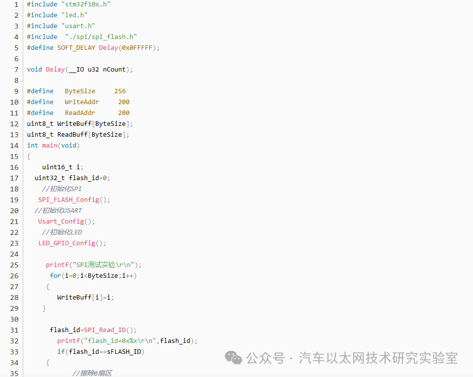
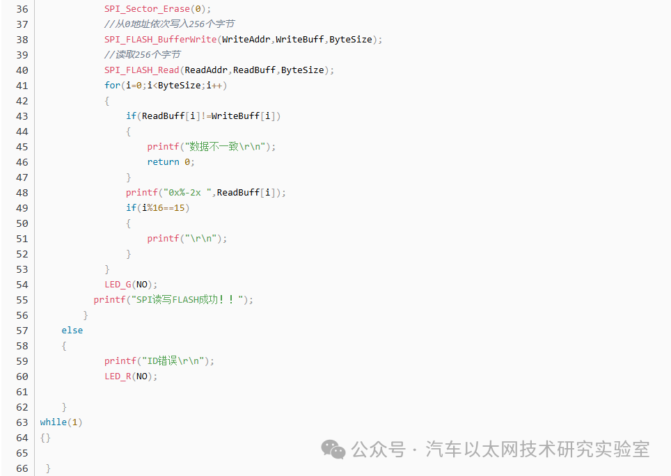
To write data to the FLASH chip according to the SPI protocol and then read it back for verification.
Experiment Principle
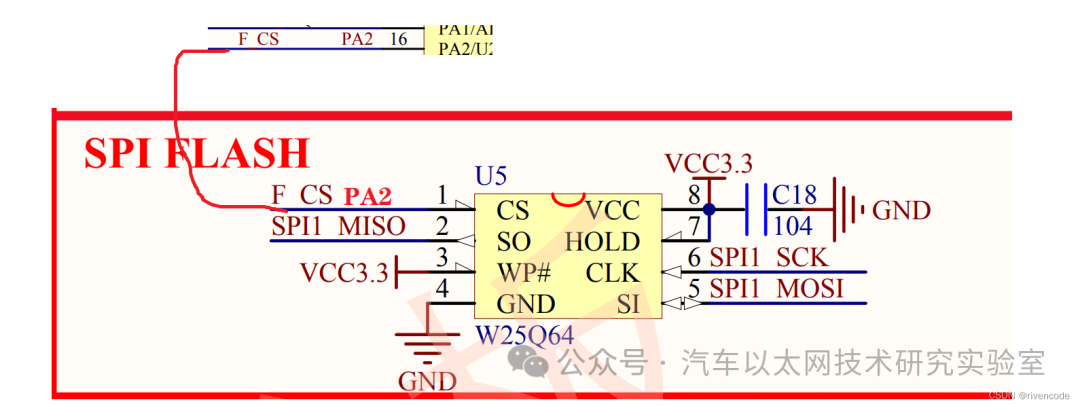
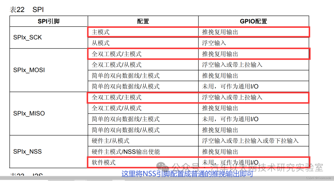
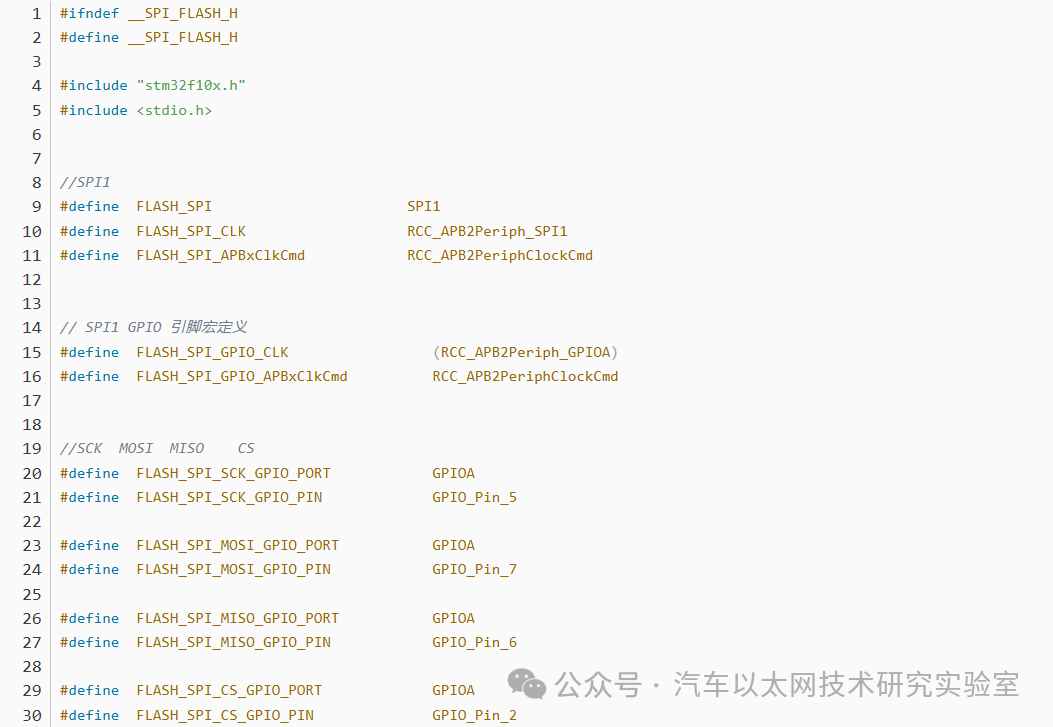
The CS/CLK/DIO/DO pins are connected to the corresponding SPI pins NSS/SCK/MOSI/MISO of the STM32, where the NSS pin of the STM32 is a regular GPIO, not a dedicated SPI NSS pin. Therefore, we need to use software control in the program; here, PA2 is used as our NSS pin to control the start and end of communication.
-
Pin Working Mode
Source Code
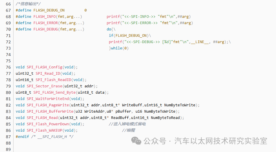
spi_flash.h
spi_flash.c
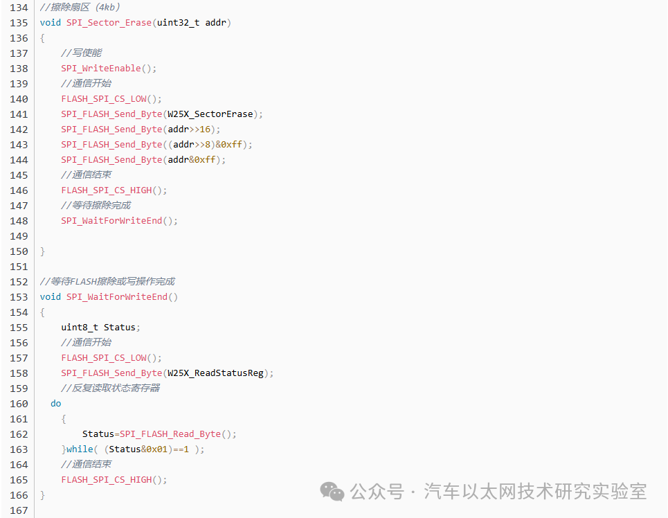
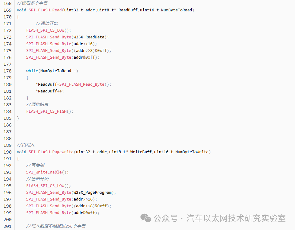
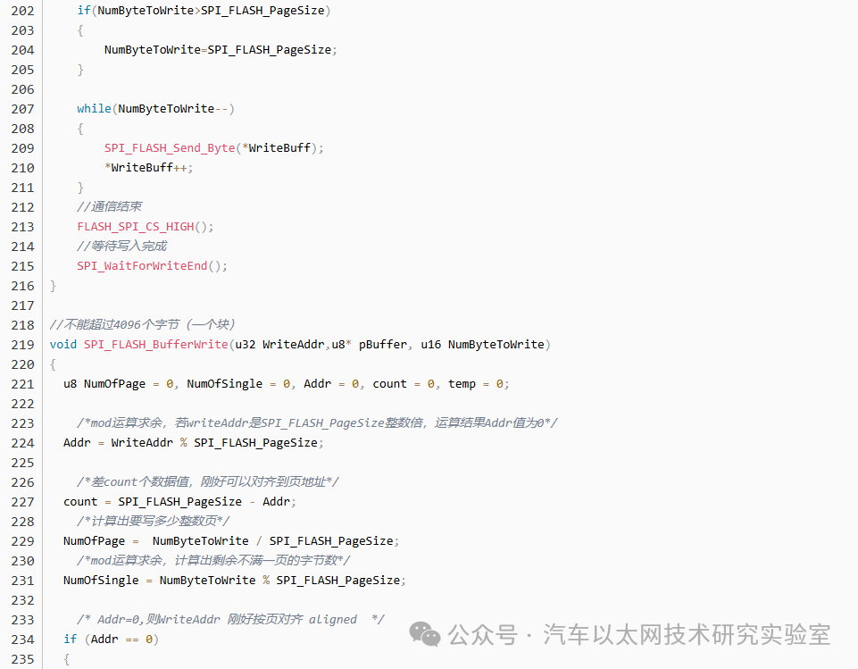
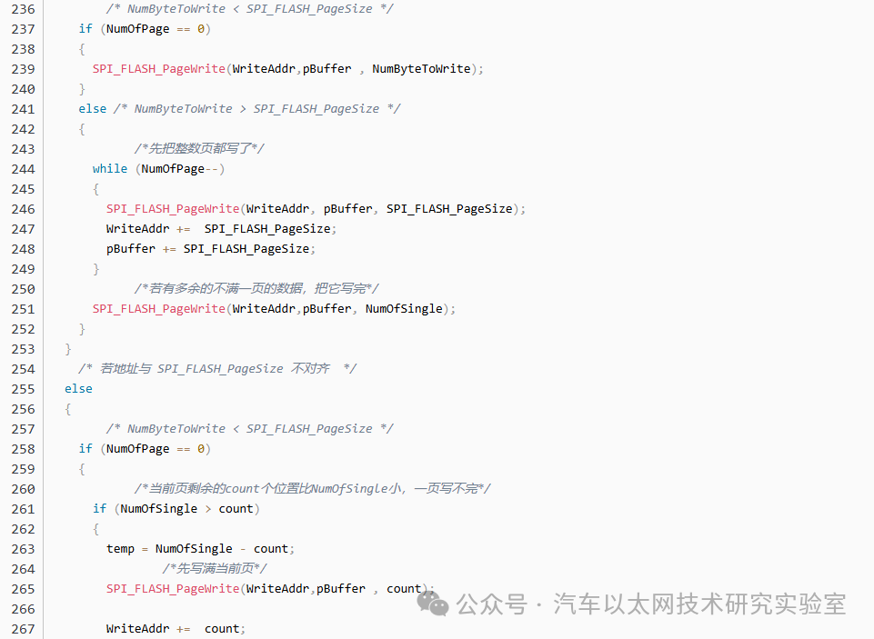
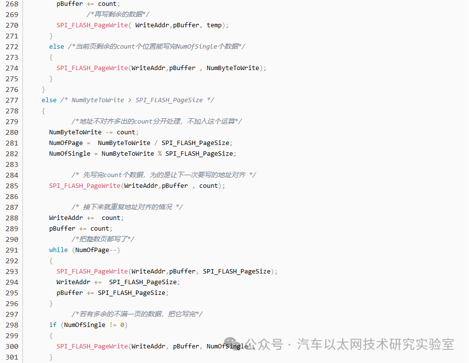
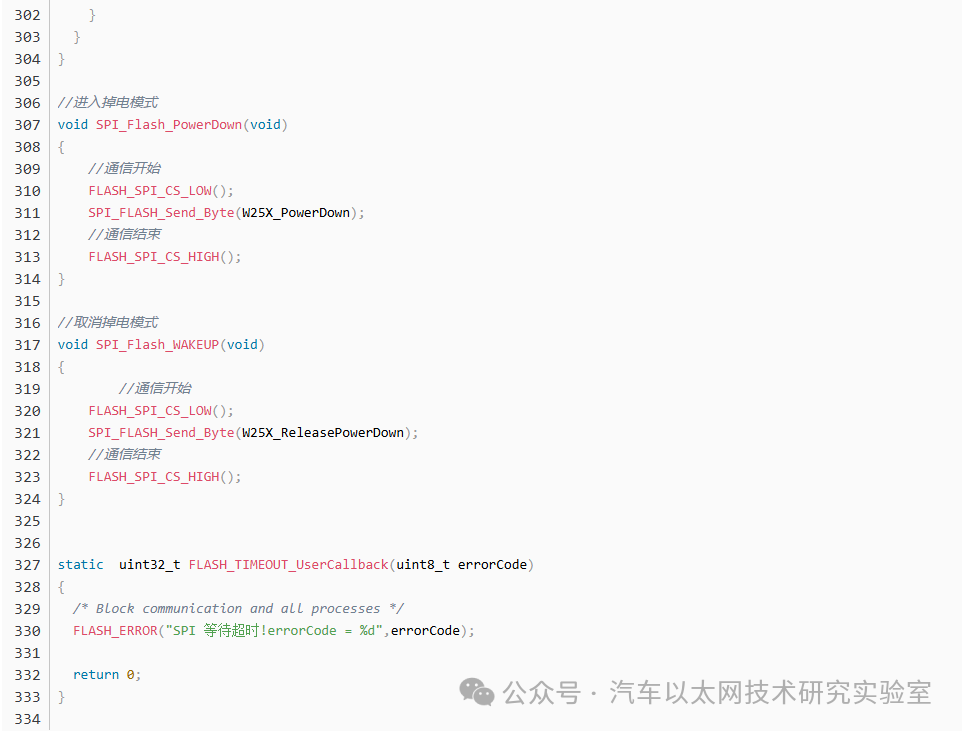
main.c





*Disclaimer: This article is original or forwarded by the author.If any party’s intellectual property rights are inadvertently infringed, please inform us for deletion.The above images and text are sourced from the internet; if there is any infringement, please contact us in a timely manner, and we will delete it within 24 hours.The content of the article represents the author’s personal views,and the Automotive Ethernet Technology Research Laboratory reprints it only to convey a different perspective, which does not representthe Automotive Ethernet Technology Research Laboratory’s endorsement or support of this view. If there are any objections, please feel free to contact the Automotive Ethernet Technology Research Laboratory.
Original link:
https://blog.csdn.net/k666499436/article/details/124882583