

The STM32 chip comes with an Ethernet module, which includes a MAC 802.3 (Media Access Control) with a dedicated DMA controller. It supports the Media Independent Interface (MII) and Reduced Media Independent Interface (RMII), and switches between the two interfaces via a selection bit (see SYSCFG_PMC register). It has an SMI interface for communication with external PHY, allowing users to select the desired mode and functionality for the MAC controller and DMA controller through a set of configuration registers.
The DMA controller connects to the core and memory via an AHB master-slave interface. The AHB master interface is used for controlling data transfers, while the AHB slave interface is used for accessing the Control and Status Register (CSR) space.
During data transmission, data is first sent from the system memory to the transmit FIFO (Tx FIFO) for buffering via DMA, and then sent by the MAC core. Similarly, the receive FIFO (Rx FIFO) stores Ethernet frames received over the line until these frames are transferred to the system memory via DMA. To understand the receipt and transmission method, let’s take a look at the STM32 Ethernet functional block diagram.
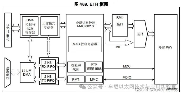
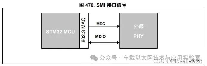
From the above diagram, it can be seen that the STM32 must connect to an external PHY chip to complete Ethernet communication. The external PHY chip can connect to the internal MAC of the STM32F4 via the MII/RMII interface and supports SMI (MDIO & MDC) interface for configuring the external Ethernet PHY chip.
Note: When using Ethernet, the AHB clock frequency must be at least 25 MHz.
Station Management Interface: SMI
The Station Management Interface (SMI) allows applications to access any PHY register via a two-wire clock and data line. This interface supports access to up to 32 PHYs. The application can select one PHY from the 32 PHYs and then select one register from the 32 registers contained in that PHY to send control data or receive status information. At any given time, only one register in one PHY can be addressed.
The MDC clock line and MDIO data line are both used as multiplexed function I/O in the microcontroller:
MDC: A periodic clock that provides reference timing for data transmission at a maximum frequency of 2.5 MHz. The minimum high and low time for MDC must both be 160 ns. The minimum period for MDC must be 400 ns. In idle state, the SMI management interface drives the MDC clock signal low.
MDIO: Data input/output bit stream used to synchronize the transmission of status information to/from the PHY device via the MDC clock signal.
SMI Frame Format
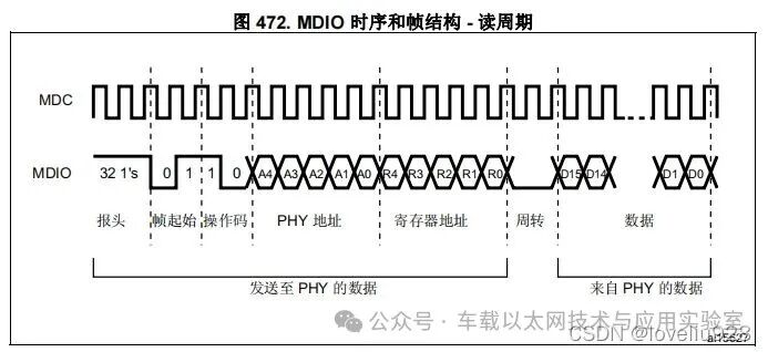
The table below shows the frame structure related to read or write operations, with bit transmission order from left to right.
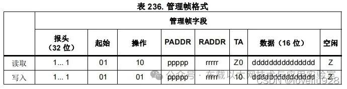
The management frame includes eight fields:
Header: Each transaction (read or write) can be initiated by the header field, which corresponds to 32 consecutive logical “1” bits on the MDIO line and 32 cycles on the MDC. This field is used to establish synchronization with the PHY device.
Start: The frame start is defined by the <01> pattern, used to verify that the line transitions from the default logical “1” state to logical “0” state, and then back from logical “0” state to logical “1” state.
Operation: Defines the type of transaction (read or write) that is occurring.
PADDR: The PHY address has 5 bits, allowing for 32 unique PHY addresses. The MSB of the address is sent and received first.
RADDR: The register address has 5 bits, allowing for addressing 32 different registers in the selected PHY device. The MSB of the address is sent and received first.
TA: The turnover field defines a 2-bit pattern between the RADDR and DATA fields to avoid contention during read transactions. During a read transaction, the MAC controller drives the 2 bits of TA to high impedance on the MDIO line. The PHY device must drive the first bit of TA to high impedance and the second bit of TA to “0”. During a write transaction, the MAC controller drives the TA field to <10> pattern. The PHY device must drive both bits of TA to high impedance.
Data: The data field is 16 bits. The bits sent and received first must be bit 15 of the ETH_MIID register.
Idle: The MDIO line is driven to high impedance. The tri-state driver must be disabled, and the PHY’s pull-up resistor keeps the line in a logical “1” state.
Based on the above image and description, we understand the communication data frame format between MAC and PHY. Next, let’s look at how STM32 defines communication registers and implements communication.
Ethernet MAC MII Address Register (ETH_MACMIIAR)
The MII address register controls the management cycle of the external PHY through the management interface.

Bits 31:16 are reserved and must be kept at reset value.
Bits 15:11 PA: PHY Address (PHY address) indicates which of the 32 possible PHY devices is being accessed.
Bits 10:6 MR: MII Register (MII register) selects the required MII register in the selected PHY device.
Bit 5 is reserved and must be kept at reset value.
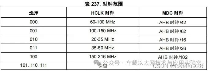
Bits 4:2 CR: Clock Range (Clock range) options determine the HCLK frequency and are used to decide the MDC clock frequency:
Option HCLK MDC Clock
000 60-100 MHz HCLK/42
001 100-150 MHz HCLK/62
010 20-35 MHz HCLK/16
011 35-60 MHz HCLK/26
100 150-168 MHz HCLK/102
101, 110, 111 Reserved –
Bit 1 MW: MII Write (MII write), when this bit is set to 1, it indicates to the PHY that a write operation using the MII data register is about to start. If this bit is not set to 1, it indicates that a read operation will be initiated, placing data into the MII data register.
Bit 0 MB: MII Busy (MII busy), this bit should read logic 0 before writing to ETH_MACMIIAR and ETH_MACMIIDR. During the write process to ETH_MACMIIAR, this bit must also be reset to 0. During PHY register access, this bit is set to 0b1 by the application, indicating that a read or write access is in progress. During a write operation to the PHY, ETH_MACMIIDR (MII data) must remain valid until the MAC clears this bit. During a read operation from the PHY, ETH_MACMIIDR is invalid until the MAC clears this bit. Only after this bit is cleared can a write to ETH_MACMIIAR (MII address) be performed.
Ethernet MAC MII Data Register (ETH_MACMIIDR)
The MAC MII data register stores the data to be written to the PHY register, with the register address specified in ETH_MACMIIAR. ETH_MACMIIDR will also store the data read from the PHY register, with the register address specified by ETH_MACMIIAR.

Bits 31:16 are reserved and must be kept at reset value.
Bits 15:0 MD: MII Data (MII data)
This contains the 16-bit data value read from the PHY after a management read operation, or the 16-bit data value to be written to the PHY before a management write operation.
SMI Clock Selection
The MAC initiates management write/read operations. The SMI clock is a divided clock whose clock source is the application clock (AHB clock). The division factor depends on the clock range set in the MII address register.
SMI Write Operation
When the application sets the MII write bit and busy bit (in the Ethernet MAC MII address register (ETH_MACMIIAR)) to 1, SMI triggers a write operation to the PHY register by transmitting the PHY address, the register address in the PHY, and the data to be written (in the Ethernet MAC MII data register (ETH_MACMIIDR)). During the transaction, the application should not change the contents of the MII address register or the MII data register. Any write operations performed on the MII address register or MII data register during this period will be ignored (the busy bit is high), and the transaction will complete without error. After the write operation is complete, SMI will indicate this by resetting the busy bit.
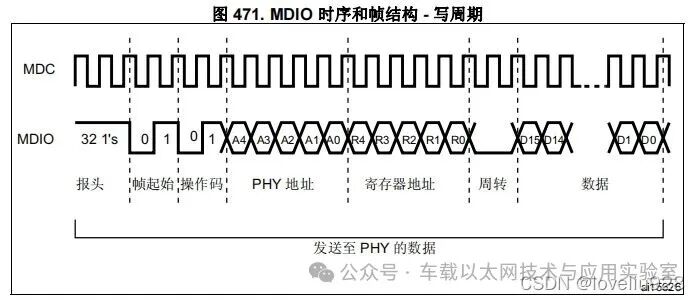
In summary, we have a general understanding of the timing process and data frame format for communication between MAC and PHY. Now let’s see how to implement the communication interface for writing PHY register operations.
-
/* Set the internal register value of the PHY chip for configuring the PHY chip */
-
* heth: eth handle, contains Ethernet register information
-
* PHYReg: PHY register address value
-
* RegValue: Register setting value
-
HAL_StatusTypeDef HAL_ETH_WritePHYRegister(ETH_HandleTypeDef *heth, uint16_t PHYReg, uint32_t RegValue)
-
{
-
uint32_t tmpreg = 0;
-
uint32_t tickstart = 0;
-
/* Get the current Ethernet controller status; if currently in read/write state, return busy information */
-
if (heth->State == HAL_ETH_STATE_BUSY_WR)
-
{
-
return HAL_BUSY;
-
}
-
/* If there is currently no read/write operation, set the state to write state */
-
heth->State = HAL_ETH_STATE_BUSY_WR;
-
/* Get the Ethernet MAC MII address register value */
-
tmpreg = heth->Instance->MACMIIAR;
-
/* Keep MDC clock, clear other bits (PA, MR, MW, MB) */
-
tmpreg &= ~ETH_MACMIIAR_CR_MASK;
-
/* Set the PHY device address */
-
tmpreg |= (((uint32_t)heth->Init.PhyAddress << 11) & ETH_MACMIIAR_PA);
-
/* Set the PHY register address */
-
tmpreg |= (((uint32_t)PHYReg << 6) & ETH_MACMIIAR_MR);
-
/* Enable write mode */
-
tmpreg |= ETH_MACMIIAR_MW;
-
/* Set the MII busy bit */
-
tmpreg |= ETH_MACMIIAR_MB;
-
/* Write the set value to the Ethernet MAC MII data register */
-
heth->Instance->MACMIIDR = (uint16_t)RegValue;
-
/* Write the set PHY address and PHY address register value to the Ethernet MAC MII address register */
-
heth->Instance->MACMIIAR = tmpreg;
-
/* Get the current time */
-
tickstart = HAL_GetTick();
-
/* Get the Ethernet busy status flag, check if data is sent successfully; during the write operation to the PHY, ETH_MACMIIDR (MII data) must remain valid until the MAC clears this bit */
-
while ((tmpreg & ETH_MACMIIAR_MB) == ETH_MACMIIAR_MB)
-
{
-
/* Timeout returns timeout status */
-
if ((HAL_GetTick() – tickstart) > PHY_WRITE_TO)
-
{
-
heth->State = HAL_ETH_STATE_READY;
-
return HAL_TIMEOUT;
-
}
-
tmpreg = heth->Instance->MACMIIAR;
-
}
-
/* Set writable operation status flag */
-
heth->State = HAL_ETH_STATE_READY;
-
/* Return operation completed */
-
return HAL_OK;
-
}
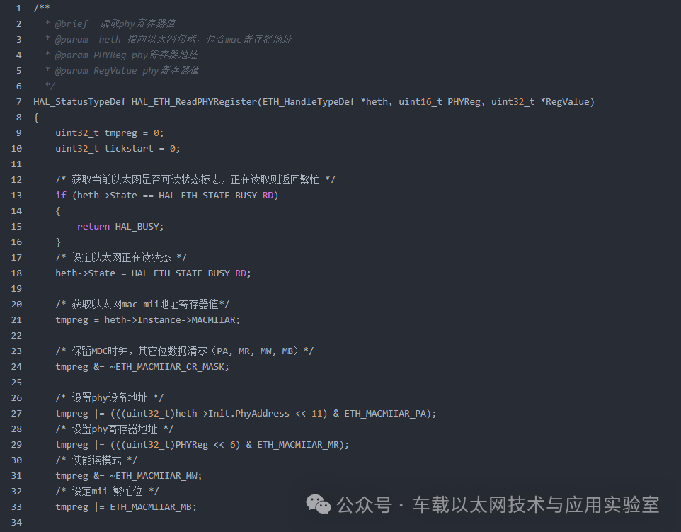
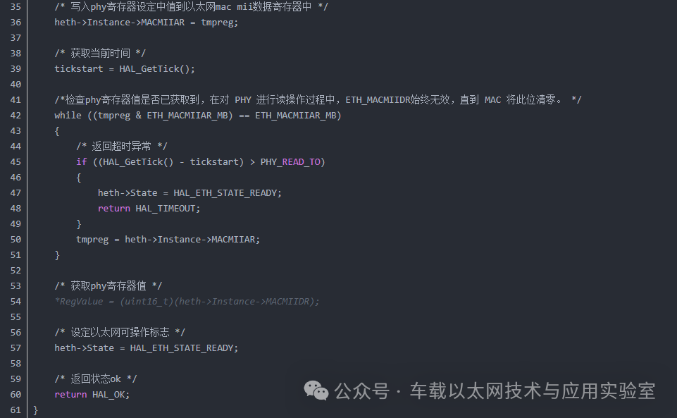
Sometimes we want to know the Ethernet link status, whether a cable is plugged in or not, and we need to perform a read operation on the PHY register. Let’s see how to implement reading the PHY register value.
SMI Read Operation
When the user sets the MII busy bit to 1 and clears the MII write bit in the Ethernet MAC MII address register (ETH_MACMIIAR), SMI triggers a read operation in the PHY register by transmitting the PHY address and the register address in the PHY. During the transaction, the application should not change the contents of the MII address register or the MII data register. Any write operations performed on the MII address register or MII data register during this period will be ignored (the busy bit is high), and the transaction will complete without error. After the read operation is complete, SMI will reset the busy bit and then update the MII data register with the data read from the PHY.


Source:
Statement: We respect originality and focus on sharing; the text and images are copyrighted by the original author. The purpose of reprinting is to share more information and does not represent the position of this account. If your rights are infringed, please contact us in a timely manner, and we will delete it as soon as possible. Thank you!
Original link:
https://blog.csdn.net/loveliu928/article/details/123857362