In modern electronic system design and development, debugging, testing, and programming are key processes to ensure product functionality and reliability. As the integration of integrated circuits (ICs) continues to increase and packaging forms become more complex (such as BGA, QFN, etc.), traditional probe testing methods have become inadequate for physically contacting chip pins. To address this challenge, JTAG (Joint Test Action Group) technology has emerged and quickly become a widely adopted standard interface in the global electronics industry. This article will systematically introduce the basic principles, core architecture, operating modes, and extensive applications of JTAG in chip design, production testing, embedded development, and secure debugging.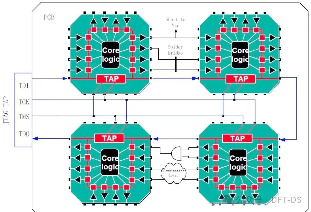
Origin and Standards of JTAG
JTAG was originally proposed by the Joint Test Action Group in the late 1980s to address the testing challenges of interconnections between chips on high-density printed circuit boards (PCBs). In 1990, IEEE officially released the IEEE 1149.1 standard, titled “Standard Test Access Port and Boundary-Scan Architecture,” marking the standardization of JTAG technology.
Since then, this standard has continuously evolved, giving rise to several extension standards, such as:
- IEEE 1149.4: Analog Boundary Scan
- IEEE 1149.6: Advanced Boundary Scan for AC Coupling and Differential Signals
- IEEE 1149.7: Compact JTAG (cJTAG), supporting a simplified interface with fewer pins
- IEEE 1532: JTAG-based In-System Programmable Standard
These standards together form a complete testing and debugging ecosystem, widely used in digital logic, FPGA, microcontrollers (MCUs), SoCs (system-on-chip), and other fields.
1. JTAG Architecture (1149.1)
JTAG stands for Joint Test Action Group, generally referring to the development group of the IEEE 1149.1 standard.
The commonly used functions of JTAG are Debug Access (through User Data Registers) and Boundary Scan (through Boundary Scan Registers).
- Debug Access is used to provide debugging tools (debugger) access to the internal interfaces of the chip (such as accessing chip registers, some control bits inside the chip, etc.). By configuring these registers or bits, the chip can be made to operate or modify configurations.
- Boundary Scan is used to implement hierarchical scanning in larger subsystems, controlling the main input data during scanning and observing the main output of the test logic to optimize and improve scanning test coverage.
The JTAG architecture generally includes the following four main components:
- Test Access Port (TAP)
- TAP Controller
- Registers
- Instruction Register
- Data Registers
- Bypass Register
- Boundary Scan Register
- Device ID Register (optional)
- User Data Registers (optional)
- Instruction Decoder
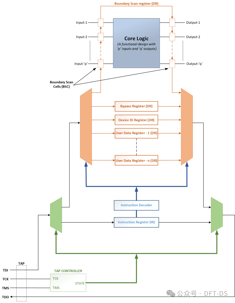 Top-level architecture of JTAG2. TAP and TAP Controller1. Test Access Port (TAP) The Test Access Port (TAP) is the interface controlled by JTAG. The IEEE standard defines four mandatory TAP signals and one optional TRST signal.TDI (Test Data Input) – used to serially feed data into the target.TDO (Test Data Output) – used to continuously collect data from the target.TCK (Test Clock) – the clock for the registers.TMS (Test Mode Select) – controls the state transitions of the TAP controller.TRST (Test Reset, optional) – resets the TAP controller.2. TAP Controller
The TAP controller is used to control the behavior of the JTAG interface. The main body of the controller is a finite state machine (FSM) with 16 states, whose state transitions are controlled by the TMS signal, as shown in Figure 2. The TAP controller can only change states on the rising edge of TCK, and the next state to which the FSM transitions is determined by the level of TMS and the current state of the FSM.
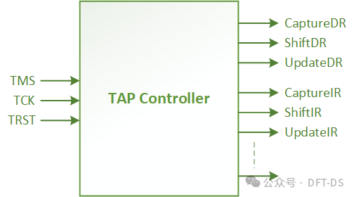 Figure 1 – Basic top-level view of the TAP controllerFigure 1 shows a very basic top-level view of the TAP controller. TMS, TCK, and the optional TRST signal enter a 16-state FSM, which generates various control signals based on the state of the FSM. These output signals include dedicated control signals for the Instruction Register (IR): CaptureIR, ShiftIR, UpdateIR and also a set of dedicated control signals for the Data Register (DR): CaptureDR, ShiftDR, UpdateDR, and other control signals.
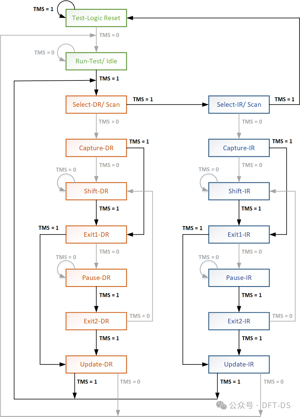 Figure 2 – TAP controller FSM state transition diagramBrief description of the different states of the TAP controller: Test-Logic-Reset: Resets the JTAG circuit. As long as the TRST (optional) signal is asserted, it will return to this state. It is also important to note that regardless of the state of the TAP controller, if TMS is set to 1 for five consecutive TCK cycles, it will return to this state. Therefore, if we do not have the TRST signal, we can still reset the circuit.Run-Test/Idle: The FSM is in a state waiting for some test operations to complete.Select-DR/Scan and Select-IR/Scan: This is a temporary state used to initiate the test data sequence for the corresponding registers (IR in the “Select-IR/Scan” state and the selected DR in the “Select-DR/Scan” state).Capture-DR and Capture-IR: In this state, data can be loaded in parallel into the corresponding registers.Shift-DR and Shift-IR: In this state, the required test data is serially loaded (or unloaded) into (or from) the corresponding registers. If we refer to the above figure, when the TAP controller is in this state, as long as TMS=0, it will remain in this state. For each clock cycle, one data bit is shifted in (or out) of the selected register through TDI (or TDO).Exit1-DR and Exit1-IR: All parallel loading (from Capture-DR and Capture-IR states) or serial loading (from Shift-DR and Shift-IR states) of data is retained in the registers in this state.Pause-DR and Pause-IR: The FSM pauses its function to wait for some external operation.Exit2-DR and Exit2-IR: This state indicates the end of the Pause-DR or Pause-IR operation and allows the TAP controller to return to the Shift-DR or Shift-IR state for more data to be shifted in (or out).Update-DR and Update-IR: In this state, the test data stored in the first flip-flop of the Register (usually each register has two flip-flops) is loaded into the second flip-flop.3. Instruction Register and Instruction Decoder1. Instruction Register (IR) The purpose of the Instruction Register is to transfer instructions via TDI and provide storage for the instructions until a new instruction is fully transferred. Typically, there are two registers inside the IR, as shown below. The hold register stores the previous instruction, while the shift register is used to shift in the next instruction without affecting the execution of the previous instruction.
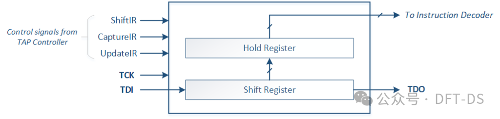 Figure 3 – Top-level view of the Data RegisterThe control signals for the Instruction Register come from the TAP controller, and depending on the FSM state, can cause the shift register to shift out (in the Shift-IR state serial update operation) or cause the contents of the shift register to be passed to the hold register (in the Update-IR state parallel update operation).
Assuming we have a 4-bit instruction register and we want to load a value, such as 1100. We must follow the steps below:
1) Control the TMS signal to input the following sequence to transition the state machine from the “Test Logic Reset” state to the “Shift-IR” state:
TMS = 0 (1st clock) TMS = 1 (2nd clock) TMS = 1 (3rd clock) TMS = 0 (4th clock) TMS = 0 (5th clock) 2) When in the “Shift-IR” state, keep TMS = 0 for the next 3 clock cycles and serially shift data (1’b1100) through TDI.
NOTE:Here, 4 bits of data are shifted in using 3 clock cycles because the LSB (least significant bit) of the data 4’b1100 appears on the TDI port after the fourth clock cycle, so when the FSM enters the “Shift-IR” state in the fifth clock cycle, the LSB will be shifted in. Ultimately, the last bit MSB (most significant bit) will be shifted in during the eighth clock cycle. Refer to the examples in the following sections for a deeper understanding of this process.
3) Control the TMS signal to input the following sequence to transition the state machine from the “Shift-IR” state to the “Update-IR” state:
TMS = 1 (9th clock) TMS = 1 (10th clock)
When the FSM enters the Update-IR state, the data (1100) in the shift register is parallel loaded into the hold register. Therefore, this instruction is now available for the instruction decoder.2. Instruction Decoder
The instruction in the Instruction Register (IR) is transferred to the instruction decoding logic, which selects the target data register for the next JTAG operation based on the instruction. Each data register is assigned a different opcode value. When a specific data register is selected, its corresponding instruction is loaded into the instruction register, and then the instruction decoder decodes that opcode and establishes a path between TDI/TDO and the corresponding data register. Assuming our JTAG module has two data registers DR-1 and DR-2, and a 4-bit wide instruction register. We will assign an opcode and corresponding instruction to each data register, such as:
DR-1 (say opcode = 4’b0010) DR-2 (say opcode = 4’b0011)
NOTE:Using a 4-bit opcode is because the JTAG instruction decoder has a width of 4 bits. If we want to access DR-2 through JTAG, we need to load the value 4’b0011 into the instruction decoder, and the instruction decoder will be able to decode that value and select DR-2.
4. Data RegistersThe basic data registers include the following:
- Boundary Scan Register (BSR)
- Bypass Register (BR)
- Device ID Register
- User Data Register(s)
Before discussing the Boundary Scan Register, it is important to first understand why we need a Boundary Scan Register.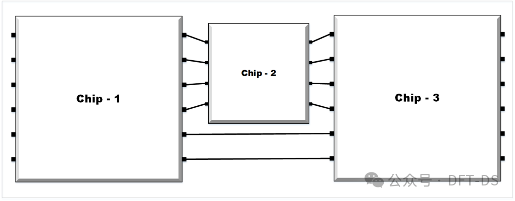
Figure 4: Schematic diagram of 3 chips on the PCB and their interconnections
Assume a scenario where we need to solder and assemble 3 chips developed and produced by different manufacturers onto the same circuit board. These chips have already been tested by their respective manufacturers using Automatic Test Equipment (ATE) before leaving the factory. However, if we encounter connectivity issues after assembling them onto the PCB, how can we detect the connection faults? If we only test for connectivity issues, we cannot send the PCB back to ATE to retest all the chips on it, as ATE is very expensive.
In the example shown in Figure 4, the IO of Chip 2 is not board-level IO. If for some debugging reason we want to access Chip 2 through its IO, how can we do that?
Boundary Scan Register (BSR)
The Boundary Scan Register is used to solve the above two problems. If all three chips support JTAG access and boundary scan, we can control and observe the IO of any device, even if they are not board-level IO. Similar to the concepts of Scan and ATPG, we can shift in the values we want into the BSR and observe the results in the BSR to test the connectivity between chips. This type of testing is called boundary scan testing.
The JTAG interface allows multiple devices to be connected to the same JTAG interface in a Daisy Chain manner. Specifically, TMS and TCK are connected in parallel to each device, while TDI and TDO are connected serially as shown in Figure 5.
Note: At any level in the system, there can only be one TAP (board-level/chip-level/IP module level). Therefore, all chips use the same TAP, rather than each chip using a dedicated TAP.
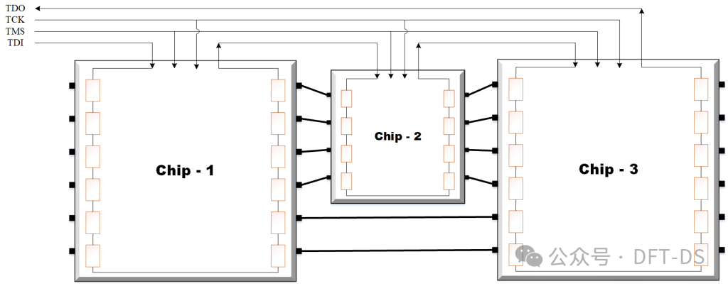
Figure 5: Boundary scan (the orange rectangles in the figure represent the boundary scan units in the chips)
Boundary Scan Registers (BSR) are inserted between the core logic of the device and the IO pins. In normal operating mode, these units are bypassed, effectively making them non-existent. In test mode, the BSR is enabled and can be used to control the IO pins and read the current values on the IO pins.
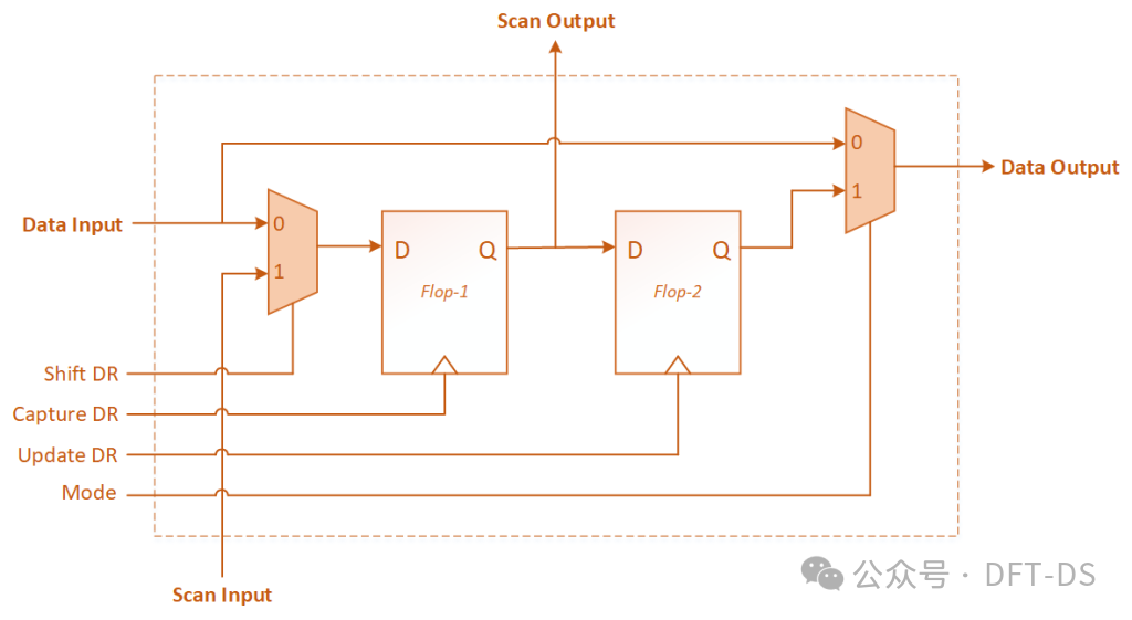
Figure 6: Internal structure of BSC
BSC supports four modes, each of which is shown in the table below.
| Operation Mode | Control signals | Control signals | Clock | Comments |
|---|---|---|---|---|
| Mode | ShiftDR | |||
| Normal | 0 | X | N/A | Functional Mode thus BSC is transparent //Normal operating mode, thus BSC is transparent. |
| Scan | X | 1 | Capture DR | Shift data from one BSC to another using the flop-1 of BSC //Shift data from one BSC to another BSC’s Flop1 |
| Update | 1 | X | Update DR | Load shifted data from flop-1 to flop-2 //Load data from Flop1 to Flop2 |
| Capture | X | 0 | Capture DR | Load data from Data Input to flop-1//Load data from input pin to Flop1 |
Bypass Register (BR)
The Bypass Register is a 1-bit wide register that provides a direct path between TDI and TDO. The existence of this direct path can minimize the test time overhead for testing devices in the circuit. Assume we have multiple serially connected chips on the PCB, as shown in Figure 7, and we want to access a single chip, such as Chip2. In the traditional approach without a bypass register, we would need to shift data through all BSCs in Chip1 and Chip3 to access the BSC in Chip2, which adds too much unnecessary shifting time overhead. To avoid the above delay, we need to bypass all BSCs in Chip1 and Chip3, so that when data passes through JTAG devices like Chip1/3, each JTAG device only requires a one-clock-cycle delay. In the above example, specifically:If we go through Chip1 and Chip3 entirely, it would require 12 + 8 + 12 = 32 clocks.But if we bypass Chip1 and Chip3, it would only require 1 + 8 + 1 = 10 clocks.When we need to bypass a chip, we need to load the opcode corresponding to the Bypass register into the instruction register, so that the instruction decoder logic establishes a bypass TDI-TDO path that only passes through the Bypass register.
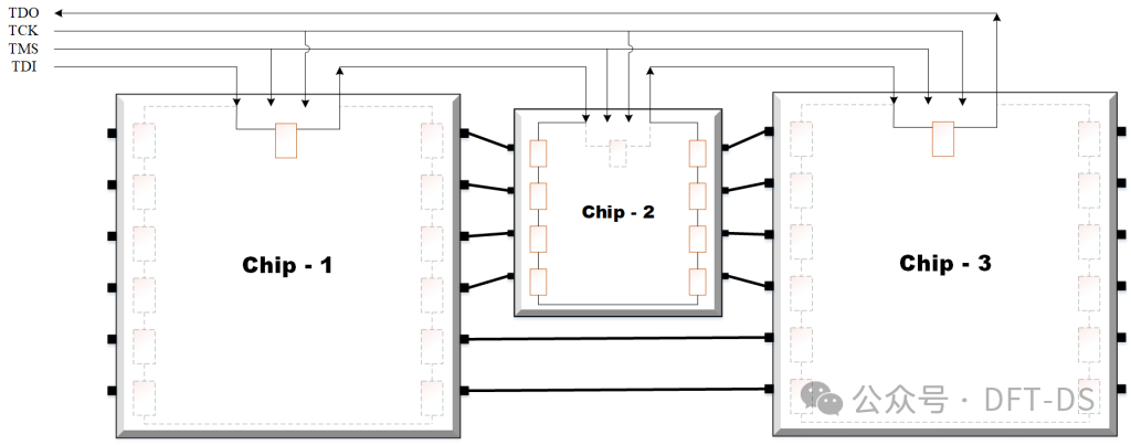 Figure 7: Example of Bypass Register usage
Device ID Register The Device ID Register is used solely for device identification. Assume we have multiple JTAG devices sharing a debug interface or TAP. To ensure we are accessing the correct debug interface, each device has an ID register, where the value (i.e., device ID code) is unique. The device ID is used to allow users or debugging tools to identify and confirm that they are accessing the correct debug interface.
User Data Register(s) These user-defined data registers are used to control or observe internal functional registers and internal ports in the core logic during debugging, as shown in Figure 8. Generally, the internal functional registers accessible via JTAG provide two sets of interfaces: one for JTAG access and another for normal functional logic access. You can refer to the JTAG access examples in the next section to understand how we access internal functional logic registers through user data registers.
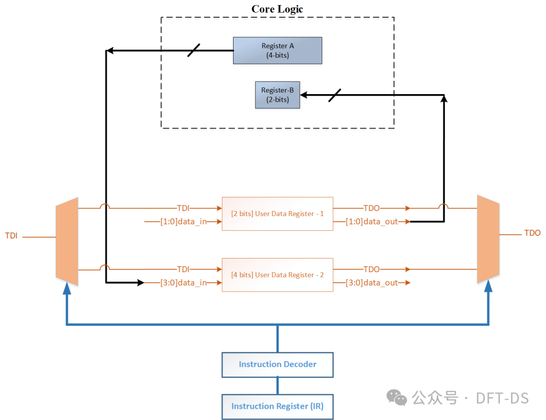 Figure 8: Schematic diagram of how to access internal functional logic registers through user data registers
Similar to the instruction register, the user data register also includes two levels of registers, as shown in Figure 9. The hold register retains the previous data, while the shift register gradually shifts in new data without affecting the current data. The control signals for the user data register come from the TAP controller, and the specific control signal values depend on the current state of the FSM, allowing the user data register’s shift register to shift in/out user data (i.e., the serial update process in the Shift-DR state) or to pass the contents of the shift register to the hold register (i.e., the parallel update process in the Update-DR state). It is worth noting that we can design multiple user data registers, each with a different opcode. When we load a specific opcode into the instruction register, the corresponding user data register will become readable and writable, allowing control and observation of the corresponding internal functional logic.
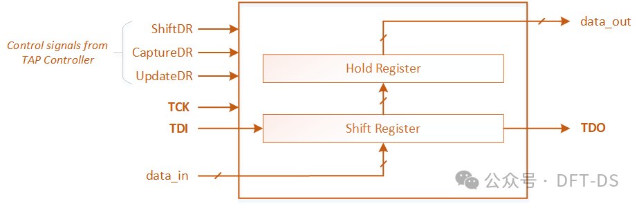 Figure 9: User Data Register schematic
5. JTAG Operation Example
Below is a complete example to understand how the TAP used for Debug access works.
Assuming a debugging scenario where we need JTAG to access and modify a 3-bit wide control signal in the design. In normal functional mode, the value of this control signal is 3’b111; however, for some debugging purposes, we want to change it to 3’b100. The following is the process to achieve this through TAP.
Assuming the JTAG instruction register (IR) in the design is 4 bits wide. First, we need to add a 3-bit wide user data register (User DR) in the JTAG design and connect its output to the control signal we want to modify. Next, we assign an opcode to this User DR, such as 4’b1010 (since the IR is 4 bits, the opcode is also 4 bits). When adding this User DR in the design, we need to set its reset value to 3’b111 (why? The reset value corresponds to the value required for the control signal in functional mode, which is 3’b111). This way, the User DR will drive this signal to 3’b111 before any JTAG Update event changes the value. Generally, during the power-up process of the chip, JTAG will exit the reset state earlier than other logic, ensuring that this signal is set to the required value of 3’b111 before the logic it drives exits the reset state.
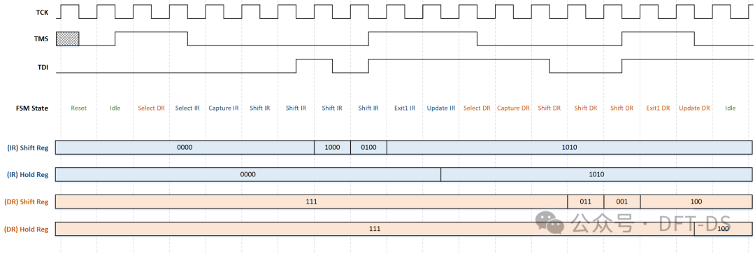
Figure 10 – Timing diagram of the example
Figure 10’s timing diagram shows how to update the value of the User DR to 3’b100. This timing diagram comes from the JTAG industrial standard, where TMS and TDI, as well as the IR/DR Hold Register, update values on the falling edge of the clock, while the FSM state and IR/DR Hold Register change values on the rising edge of the clock.In Figure 10, the 16-state FSM starts working from the Test-Logic Reset state, transitioning the state machine into the Shift IR state by setting the timing of TMS. Next, the opcode corresponding to the data register (4’b1010) is shifted into the instruction register through the TDI port.
The initial values of the shift and hold registers are both reset values 0, and 4’b1010 is serially shifted into the instruction register from LSB to MSB order. By setting the timing of TMS, the state machine transitions into the Update IR state. In the Update IR state, the hold register of the IR is updated with the value from the shift register, and the instruction decoder decodes the value of that instruction, establishing a path between TDI and the user data register.
Next, the FSM exits the Update IR state and transitions to the Shift DR state, where the desired value 3’b100 is serially shifted into the DR shift register from LSB to MSB order. Once the data 3’b100 is fully loaded into the shift register, the FSM jumps to the Update DR state. In this state, the DR hold register is updated to 3’b100, and at this moment, the value of the control signal that needs to be modified also changes from the reset value 3’b111 to 3’b100.
6. Main Applications of JTAG
1. Production Testing and Fault Diagnosis
After PCB manufacturing is completed, using JTAG for boundary scan testing is an efficient means to verify solder quality and interconnection integrity. Compared to traditional flying probe testing, JTAG testing is faster and has higher coverage, especially suitable for high-density, multi-layer board designs.
2. In-System Programming (ISP)
Many FPGAs, CPLDs, and MCUs support firmware programming through the JTAG interface. Developers can directly update program code without removing the chip from the circuit board, greatly improving development efficiency and on-site maintenance capabilities.
3. Embedded System Debugging
JTAG is the most commonly used hardware debugging interface in embedded development. In conjunction with debuggers (such as J-Link, ULINK, OpenOCD, etc.), developers can achieve:
- Access to CPU Registers: Read and write program counters, stack pointers, and other core registers.
- Memory Access: View or modify RAM and Flash contents.
- Breakpoints and Single-Step Execution: Set hardware breakpoints and execute instructions one by one.
- Real-Time Monitoring: Observe variable changes and function call flows.
For example, in ARM architecture, the CoreSight debugging architecture widely uses JTAG or its simplified version SWD (Serial Wire Debug) for deep debugging.
4. Chip Verification and Functional Testing
During the chip design phase, JTAG can be used to verify the functionality of internal modules of SoCs, such as bus interfaces, DMA controllers, peripherals, etc. By accessing internal registers through JTAG, normal software processes can be bypassed to directly test hardware logic.
5. Security and Reverse Engineering (Double-Edged Sword)
The JTAG interface brings convenience but also poses security risks. Attackers may exploit the JTAG interface to:
- Read encryption keys or sensitive data
- Bypass secure boot mechanisms
- Inject malicious code
Therefore, many security-sensitive devices (such as smart cards, payment terminals) will disable or lock the JTAG interface during mass production or close debugging functions through OTP (One-Time Programmable) fuses.
Conclusion
As an indispensable testing and debugging infrastructure in electronic system design, JTAG has maintained its strong vitality after more than thirty years of development. It not only solves the bottlenecks of traditional testing methods but also provides strong support for the development, verification, and maintenance of modern complex SoCs. For electronic engineers, mastering the basic principles and application methods of JTAG is an essential skill for efficient development and reliable testing. In the future, as the integration of chips and the complexity of systems continue to increase, JTAG and its derived technologies will continue to play a key role in ensuring the quality and security of electronic systems.