Write a technical article and share in a prize pool of thousands! Come and share your EMC rectification insights.
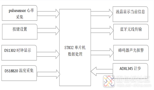
Health Bracelet Design Based on STM32 MicrocontrollerOverall System Framework
The hardware part of this system mainly consists of a sensor module, Bluetooth module, clock module, STM32 microcontroller, alarm circuit, and button circuit. In addition, there is an APP on the mobile end that communicates with the Bluetooth module. The sensor module, circuit, Bluetooth APP, and the compiled program in Keil software together form the entire health bracelet system. The overall framework of the system is shown in Figure 0.
Figure 0 System Framework Physical Diagram: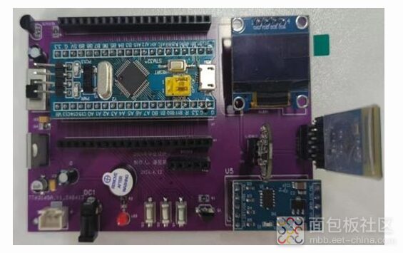 Schematic Diagram:
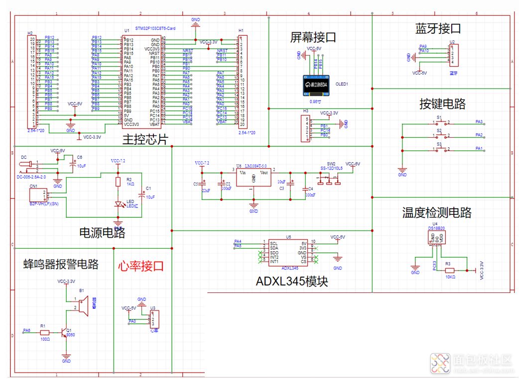 1. Introduction to STM32 Microcontroller
The STM32 series processors developed by the well-known semiconductor company (STMicroelectronics) are 32-bit microcontrollers based on the ARM7 architecture. When choosing this control chip, I was not simply pursuing cost or power consumption optimization, but rather to construct the necessary peripheral expansion circuits for various experimental functions, providing more diverse interfaces and functions while ensuring the realization of design functions. It is worth mentioning that after studying the microcontroller course, due to its intuitive operation interface and friendly programming environment, this control chip is relatively easy to get started with.
In this design, the STM32F103C8T6 microcontroller is selected as the main control unit. Compared to the traditional 51 series microcontrollers, the C8T6 exhibits significant advantages in multiple aspects. First, in terms of operating speed, the performance of the C8T6 far exceeds that of the 51 microcontroller. This is thanks to its high-performance ARM Cortex-M3 core, with a main frequency of up to 72MHz, ensuring faster and more efficient instruction execution and data processing capabilities. This allows the C8T6 to easily handle complex tasks and applications with high real-time requirements. Secondly, the C8T6 has two built-in AD converters, which is another major advantage over the 51 microcontroller. The AD converter (analog-to-digital converter) can convert continuous analog signals into discrete digital signals, which is crucial in many applications. For example, analog signals such as sound volume, temperature, humidity, and light intensity can be converted into digital signals through the AD converter, which can then be processed and controlled by the microcontroller. The two AD converters of the C8T6 can work simultaneously, improving the efficiency and accuracy of data collection, meeting the processing needs of various analog signals in complex systems. In addition, the C8T6 also has other rich peripheral interfaces and functions, such as GPIO, USART, SPI, I2C, etc., providing designers with more choices and flexibility. At the same time, its low-power design and various power-saving modes also help extend the overall operating time of the device, reducing the system’s energy consumption. Its pin function diagram is shown in Figure 1.
1. Introduction to STM32 Microcontroller
The STM32 series processors developed by the well-known semiconductor company (STMicroelectronics) are 32-bit microcontrollers based on the ARM7 architecture. When choosing this control chip, I was not simply pursuing cost or power consumption optimization, but rather to construct the necessary peripheral expansion circuits for various experimental functions, providing more diverse interfaces and functions while ensuring the realization of design functions. It is worth mentioning that after studying the microcontroller course, due to its intuitive operation interface and friendly programming environment, this control chip is relatively easy to get started with.
In this design, the STM32F103C8T6 microcontroller is selected as the main control unit. Compared to the traditional 51 series microcontrollers, the C8T6 exhibits significant advantages in multiple aspects. First, in terms of operating speed, the performance of the C8T6 far exceeds that of the 51 microcontroller. This is thanks to its high-performance ARM Cortex-M3 core, with a main frequency of up to 72MHz, ensuring faster and more efficient instruction execution and data processing capabilities. This allows the C8T6 to easily handle complex tasks and applications with high real-time requirements. Secondly, the C8T6 has two built-in AD converters, which is another major advantage over the 51 microcontroller. The AD converter (analog-to-digital converter) can convert continuous analog signals into discrete digital signals, which is crucial in many applications. For example, analog signals such as sound volume, temperature, humidity, and light intensity can be converted into digital signals through the AD converter, which can then be processed and controlled by the microcontroller. The two AD converters of the C8T6 can work simultaneously, improving the efficiency and accuracy of data collection, meeting the processing needs of various analog signals in complex systems. In addition, the C8T6 also has other rich peripheral interfaces and functions, such as GPIO, USART, SPI, I2C, etc., providing designers with more choices and flexibility. At the same time, its low-power design and various power-saving modes also help extend the overall operating time of the device, reducing the system’s energy consumption. Its pin function diagram is shown in Figure 1. 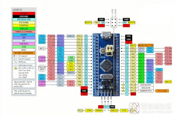 Figure 1 STM32F103C8T6 Pin Function Diagram
In summary, the STM32F103C8T6 microcontroller, with its excellent performance, rich function set, and efficient AD converters, has been selected as the core control unit in this design, providing stable, reliable, and efficient control capabilities for the entire system without the need to add an external ADC module, greatly facilitating users. In addition, the STM32 microcontroller supports multiple clock operating modes, giving it a wide range of application prospects in power-sensitive products. Its physical appearance is shown in Figure 2.
Figure 1 STM32F103C8T6 Pin Function Diagram
In summary, the STM32F103C8T6 microcontroller, with its excellent performance, rich function set, and efficient AD converters, has been selected as the core control unit in this design, providing stable, reliable, and efficient control capabilities for the entire system without the need to add an external ADC module, greatly facilitating users. In addition, the STM32 microcontroller supports multiple clock operating modes, giving it a wide range of application prospects in power-sensitive products. Its physical appearance is shown in Figure 2. 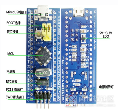 Figure 2 STM32F103C8T6 Physical Diagram
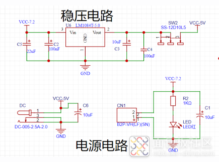
2. Power Supply Circuit Design
This design has two power supply methods. One is to use 5V DC power supply for easy debugging. The second is to use a 7.2V lithium battery with a voltage regulator circuit to output 5V to power the entire system, which is convenient for testing functions such as step counting. The switch is used to control whether the 5V voltage powers the system. Among them, DC and CN1 are power interfaces, SW is the circuit switch, LED is the power indicator, C1, C3, C5, C6 are compensation capacitors, and C4 is the power filtering capacitor. Its circuit structure is shown in Figure 3.
Figure 3 Power Interface Circuit Diagram
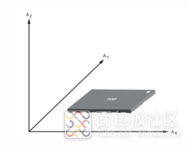
By studying the walking patterns of humans, it is found that three-direction accelerations are generated when a person walks. Using an accelerometer to capture the three-direction accelerations of a person walking can simulate the vertical, forward, and lateral accelerations generated when running. According to surveys, the normal stride of a person is approximately between 50 to 80 centimeters, with fluctuations in this range due to factors such as height and walking speed. For the accuracy of step counting, this design uses the ADXL345 module. This is a 5V powered three-axis accelerometer with high resolution and variable measurement range characteristics. This sensor can measure acceleration values along the x, y, and z axes, with a scale factor of 3.9mg/lsb. It is important to note that the direction of the X, Y, and Z axes depends on the placement of the chip. The detection axes of the ADXL345 sensor are shown in Figure 3.
Figure 3 ADXL345 Detection Axes Diagram
During human motion, one of the axes of the three-axis acceleration generally exhibits significant activity. Through experimental observation and analysis of chip placement combinations, we found that the peak value of the Y-axis acceleration is more pronounced during movement. We can determine the acceleration and acceleration amplitude during exercise through multiple measurements. To judge the motion state, we compared the acceleration values measured by the ADXL345 with the acceleration threshold obtained after multiple experiments. If the acceleration value exceeds this threshold, the bracelet is considered to be in a tilted state, and we recognize it as a motion state, simultaneously starting to count steps and calculating the walking distance based on the relationship between the number of steps and stride length. The formula is:
where S is the distance, N is the number of steps, and L is the stride length.
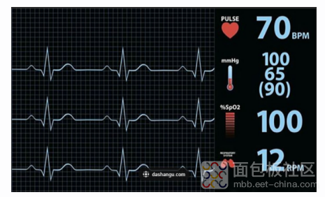
The heart rate is the number of heartbeats per minute, which is an intuitive and convenient way to assess personal health status and measure exercise intensity. As a vital sign of the human body, its value varies from person to person, depending on age, gender, and other physiological characteristics. Generally speaking, a healthy adult at rest maintains a heart rate of about 75 beats per minute, although this value fluctuates between 60 to 100 beats per minute. The normal heart rate is shown in Figure 4.
Figure 4 Normal Heart Rate Diagram
The Pulsesensor is a biosensor module that determines human heart rate based on the principle of photoelectric reflection. By clamping the heart rate sensor with a fingertip, infrared light or LED light of a specific wavelength illuminates the skin. When the light passes through the peripheral blood vessels of the body, the transparency of this light changes due to the volume change of arterial pulsation. At this time, the photoelectric converter receives the light reflected by the human tissue and converts it into an electrical signal. The collected data is then transmitted to the STM32 microcontroller through the signal output port. After inputting the data, the microcontroller directly calculates the time between the peaks of two adjacent pulse waves and filters it to obtain the time between two heartbeats, which is the BI value. Through the simple calculation BPM (heart rate) = 60/BI, the heart rate value can be obtained. The heart rate detection function of the Pulsesensor module provides important data support for the medical and health fields, while also offering convenience and assurance for people’s lives and health. The waveform measured by the Pulsesensor sensor in the digital oscilloscope is shown in Figure 5.
Figure 2 STM32F103C8T6 Physical Diagram
2. Power Supply Circuit Design
This design has two power supply methods. One is to use 5V DC power supply for easy debugging. The second is to use a 7.2V lithium battery with a voltage regulator circuit to output 5V to power the entire system, which is convenient for testing functions such as step counting. The switch is used to control whether the 5V voltage powers the system. Among them, DC and CN1 are power interfaces, SW is the circuit switch, LED is the power indicator, C1, C3, C5, C6 are compensation capacitors, and C4 is the power filtering capacitor. Its circuit structure is shown in Figure 3.
Figure 3 Power Interface Circuit Diagram
By studying the walking patterns of humans, it is found that three-direction accelerations are generated when a person walks. Using an accelerometer to capture the three-direction accelerations of a person walking can simulate the vertical, forward, and lateral accelerations generated when running. According to surveys, the normal stride of a person is approximately between 50 to 80 centimeters, with fluctuations in this range due to factors such as height and walking speed. For the accuracy of step counting, this design uses the ADXL345 module. This is a 5V powered three-axis accelerometer with high resolution and variable measurement range characteristics. This sensor can measure acceleration values along the x, y, and z axes, with a scale factor of 3.9mg/lsb. It is important to note that the direction of the X, Y, and Z axes depends on the placement of the chip. The detection axes of the ADXL345 sensor are shown in Figure 3.
Figure 3 ADXL345 Detection Axes Diagram
During human motion, one of the axes of the three-axis acceleration generally exhibits significant activity. Through experimental observation and analysis of chip placement combinations, we found that the peak value of the Y-axis acceleration is more pronounced during movement. We can determine the acceleration and acceleration amplitude during exercise through multiple measurements. To judge the motion state, we compared the acceleration values measured by the ADXL345 with the acceleration threshold obtained after multiple experiments. If the acceleration value exceeds this threshold, the bracelet is considered to be in a tilted state, and we recognize it as a motion state, simultaneously starting to count steps and calculating the walking distance based on the relationship between the number of steps and stride length. The formula is:
where S is the distance, N is the number of steps, and L is the stride length.
The heart rate is the number of heartbeats per minute, which is an intuitive and convenient way to assess personal health status and measure exercise intensity. As a vital sign of the human body, its value varies from person to person, depending on age, gender, and other physiological characteristics. Generally speaking, a healthy adult at rest maintains a heart rate of about 75 beats per minute, although this value fluctuates between 60 to 100 beats per minute. The normal heart rate is shown in Figure 4.
Figure 4 Normal Heart Rate Diagram
The Pulsesensor is a biosensor module that determines human heart rate based on the principle of photoelectric reflection. By clamping the heart rate sensor with a fingertip, infrared light or LED light of a specific wavelength illuminates the skin. When the light passes through the peripheral blood vessels of the body, the transparency of this light changes due to the volume change of arterial pulsation. At this time, the photoelectric converter receives the light reflected by the human tissue and converts it into an electrical signal. The collected data is then transmitted to the STM32 microcontroller through the signal output port. After inputting the data, the microcontroller directly calculates the time between the peaks of two adjacent pulse waves and filters it to obtain the time between two heartbeats, which is the BI value. Through the simple calculation BPM (heart rate) = 60/BI, the heart rate value can be obtained. The heart rate detection function of the Pulsesensor module provides important data support for the medical and health fields, while also offering convenience and assurance for people’s lives and health. The waveform measured by the Pulsesensor sensor in the digital oscilloscope is shown in Figure 5.
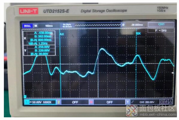 Figure 5 Pulsesensor Sensor Waveform Diagram
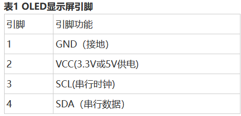
LED (Organic Light Emitting Diode) displays occupy an important position in display technology due to their unique advantages, especially in portable devices such as smartphones and tablets. OLED displays have characteristics such as self-emission, wide viewing angles, vibrant colors, and flexibility, making them a leading emerging application technology in the future flat display technology revolution. In this design, a 0.96-inch OLED display is used, communicating via standard IIC. Its pin function is shown in Table 1:
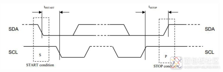
When setting up the display, the startup condition is established by pulling the SCL data line from high to low while keeping the SDA clock line high; the stop condition is established by pulling the SDA clock line from low to high. Its timing diagram is shown in Figure 6.
Figure 6 OLED Timing Diagram
5. DS18B20 Temperature Detection
According to medical research, the normal range of wrist temperature in humans is between 36-37.3 degrees Celsius. If it exceeds this temperature, it may indicate a fever. For the accuracy of temperature measurement, this design uses the DS18B20 temperature sensor. It is powered by a front-end 3.3V circuit, which aims to digitize the output voltage signal fully, thus eliminating the need to design an A/D conversion circuit for analog signals, greatly simplifying the circuit design and reducing temperature measurement errors. Compared to traditional temperature measurement devices such as thermistors, the single-bus data transmission method of the DS18B20 is particularly prominent, being both convenient and simple. Due to the “one-wire bus” feature of the DS18B20, as a slave, it can connect to the IO port of the STM32F103C8T6 through only one data line, enabling efficient data transmission. Its specific parameters are shown in Table 2:
Figure 5 Pulsesensor Sensor Waveform Diagram
LED (Organic Light Emitting Diode) displays occupy an important position in display technology due to their unique advantages, especially in portable devices such as smartphones and tablets. OLED displays have characteristics such as self-emission, wide viewing angles, vibrant colors, and flexibility, making them a leading emerging application technology in the future flat display technology revolution. In this design, a 0.96-inch OLED display is used, communicating via standard IIC. Its pin function is shown in Table 1:
When setting up the display, the startup condition is established by pulling the SCL data line from high to low while keeping the SDA clock line high; the stop condition is established by pulling the SDA clock line from low to high. Its timing diagram is shown in Figure 6.
Figure 6 OLED Timing Diagram
5. DS18B20 Temperature Detection
According to medical research, the normal range of wrist temperature in humans is between 36-37.3 degrees Celsius. If it exceeds this temperature, it may indicate a fever. For the accuracy of temperature measurement, this design uses the DS18B20 temperature sensor. It is powered by a front-end 3.3V circuit, which aims to digitize the output voltage signal fully, thus eliminating the need to design an A/D conversion circuit for analog signals, greatly simplifying the circuit design and reducing temperature measurement errors. Compared to traditional temperature measurement devices such as thermistors, the single-bus data transmission method of the DS18B20 is particularly prominent, being both convenient and simple. Due to the “one-wire bus” feature of the DS18B20, as a slave, it can connect to the IO port of the STM32F103C8T6 through only one data line, enabling efficient data transmission. Its specific parameters are shown in Table 2:
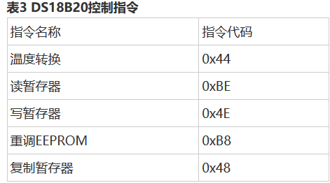
 The command code for temperature detection is shown in Table 3:
 DS1302 is a real-time clock chip manufactured by the American Dallas company, which integrates high performance, low power consumption, and built-in RAM. Its characteristics include microcurrent charging capability. This chip uses a common 32.76kHz crystal oscillator, which can accurately record year, month, day, week, hour, minute, and second, and has a leap year automatic compensation function. Its operating voltage range is between 2.5-5.5V, allowing it to work stably under various power conditions to meet different application needs. Within this voltage range, the DS1302 can accurately keep time, provide stable clock signals, and maintain low power operation, suitable for various situations requiring accurate time management and strict power consumption requirements. Communication between the DS1302 and CPU is achieved through a three-wire interface for synchronous communication, which not only supports burst mode but also allows multiple bytes of clock or RAM data to be transmitted in one go, greatly enhancing data transmission efficiency. Meanwhile, the DS1302 integrates up to 31 bytes of RAM storage, providing ample space for data storage. To meet diverse power requirements, the DS1302 is specially designed with dual power pins and has the capability for microcurrent charging of backup power, ensuring stable operation in different power environments. In terms of data transmission, it employs a serial method that not only provides programmable charging functions for power loss protection but also allows users to turn off the charging function as needed. Its internal structure is shown in Figure 7.
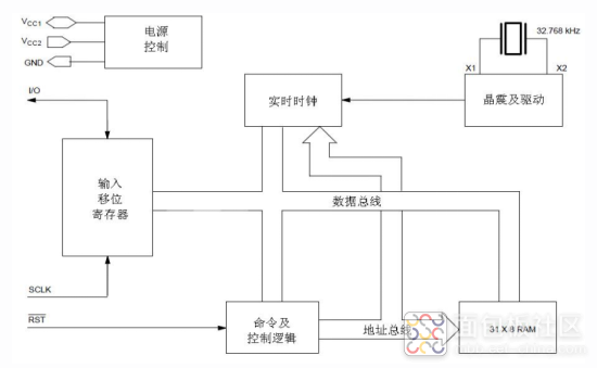 Figure 7 DS1302 Internal Structure Diagram
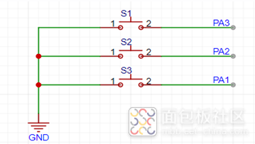
7. Button Setting Circuit
This design has a total of 3 control command buttons: parameter setting; increase setting; decrease setting; in addition, there is a confirmation button. These three buttons can be used to set the parameters of the system, such as setting the alarm threshold for heart rate. One end of the button is grounded, and low level is used as the effective signal. When the button is pressed, the corresponding circuit will be connected. To eliminate button bouncing, I chose a software debouncing method. When the button closure is detected, a subroutine is called to execute a delay function; similarly, when the button is released, a delay of several milliseconds will also be executed to eliminate bouncing. Its circuit diagram is shown in Figure 8.
Figure 8 Button Circuit Diagram
The buttons can be used to set the upper and lower limits of heart rate and body temperature, and when the parameters are out of range, the buzzer will sound an alarm. The buzzer, as a sound-emitting component, will emit a beep when powered on, making it quite convenient to operate. There are many types of buzzers on the market, and we specifically chose those that support 5V power supply, which have shown high practicality in actual applications. In this design, when the system detects that the temperature or heart rate exceeds the preset alarm threshold, the buzzer will sound an alarm. The circuit design for the buzzer consists of three parts: a 1k resistor, an NPN transistor, and the buzzer itself. The main reason for choosing the NPN transistor is its current and level amplification function, thus it is necessary to utilize the transistor’s current and level amplification characteristics to drive the buzzer. Its schematic diagram is shown in Figure 9.
Figure 7 DS1302 Internal Structure Diagram
7. Button Setting Circuit
This design has a total of 3 control command buttons: parameter setting; increase setting; decrease setting; in addition, there is a confirmation button. These three buttons can be used to set the parameters of the system, such as setting the alarm threshold for heart rate. One end of the button is grounded, and low level is used as the effective signal. When the button is pressed, the corresponding circuit will be connected. To eliminate button bouncing, I chose a software debouncing method. When the button closure is detected, a subroutine is called to execute a delay function; similarly, when the button is released, a delay of several milliseconds will also be executed to eliminate bouncing. Its circuit diagram is shown in Figure 8.
Figure 8 Button Circuit Diagram
The buttons can be used to set the upper and lower limits of heart rate and body temperature, and when the parameters are out of range, the buzzer will sound an alarm. The buzzer, as a sound-emitting component, will emit a beep when powered on, making it quite convenient to operate. There are many types of buzzers on the market, and we specifically chose those that support 5V power supply, which have shown high practicality in actual applications. In this design, when the system detects that the temperature or heart rate exceeds the preset alarm threshold, the buzzer will sound an alarm. The circuit design for the buzzer consists of three parts: a 1k resistor, an NPN transistor, and the buzzer itself. The main reason for choosing the NPN transistor is its current and level amplification function, thus it is necessary to utilize the transistor’s current and level amplification characteristics to drive the buzzer. Its schematic diagram is shown in Figure 9.
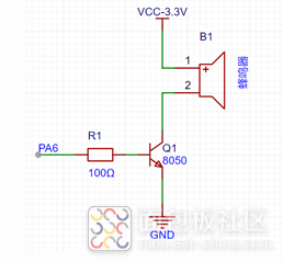 Figure 9 Buzzer Alarm Schematic Diagram
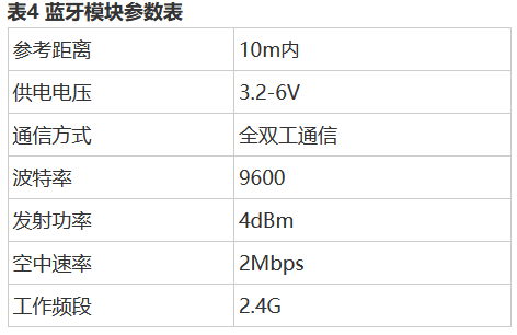
9. Bluetooth Transmission Module
In this design, the main function of the Bluetooth transmission module is to synchronize and send information such as body temperature, heart rate, and step count to the APP on the mobile end, allowing trainers to gain a more intuitive understanding of the physiological indicators of the bracelet wearer. The parameters of the HC05 Bluetooth module are shown in Table 4:
Source: Breadboard Community czd886 share
Figure 9 Buzzer Alarm Schematic Diagram
9. Bluetooth Transmission Module
In this design, the main function of the Bluetooth transmission module is to synchronize and send information such as body temperature, heart rate, and step count to the APP on the mobile end, allowing trainers to gain a more intuitive understanding of the physiological indicators of the bracelet wearer. The parameters of the HC05 Bluetooth module are shown in Table 4:
Source: Breadboard Community czd886 share
Collection of Circuit Diagrams
Common Analog Circuits | Operational Amplifier Circuits | Protection Circuits | EMC Standard Circuits | Power Supply Circuit Collection | Practical Control Circuits | Microcontroller Application Circuits | Waveform Generation Circuits | Automotive Circuit Diagram Collection | 555 Circuit | Small Appliance Circuits | 9 Basic Module Circuits | Schematic Abbreviations | Circuit Symbols
Circuit Basics | Digital Circuits | Oscilloscope Basics | Multimeter Usage | Signal Integrity | Ground Knowledge | Embedded Basics | STM32 Basic Knowledge Summary | C Language Key Points
Resistor | Capacitor | Inductor | Diode | Transistor | TVS | Thyristor | MOSFET | IGBT | Sensor | Relay | Equivalent Circuit of Components | Complete Guide to Component Selection | Component Failure
If you want to join the relevant electronic industry community, you can scan the QR code to add our community operation colleagues. Please note your group entry needs and keywords. (Keywords refer to the target technical field)