In the landscape of silicon carbide (SiC) power devices, SiC MOSFET is undoubtedly the brightest star. From traction inverters in new energy vehicles to photovoltaic inverters, from energy storage systems to industrial power supplies, it continuously drives technological innovation in the field of power electronics with its high frequency, high efficiency, and high temperature resistance characteristics. When it comes to the research and production of SiC MOSFETs, there is a general consensus in the industry: high-quality substrates and epitaxial wafers can now be sourced externally, laying a solid foundation for device manufacturing. However, what truly determines the performance limits of the device is not these basic materials, but the design philosophy and precision manufacturing processes that run throughout. On the tiny chip, every structural layout and every slight adjustment of process parameters can lead to significant performance differences. Today, we will delve into the internal structure of SiC MOSFETs, dissecting the core elements of their layout design and exploring the technical logic behind high-performance devices.
Chip Layout
When we receive a manufactured and tested SiC MOSFET wafer, the first thing we see is a neatly arranged array of chips (as shown in Figure 1). Although these chips are small in size, their surface layout conceals secrets, with each area carrying specific functions.
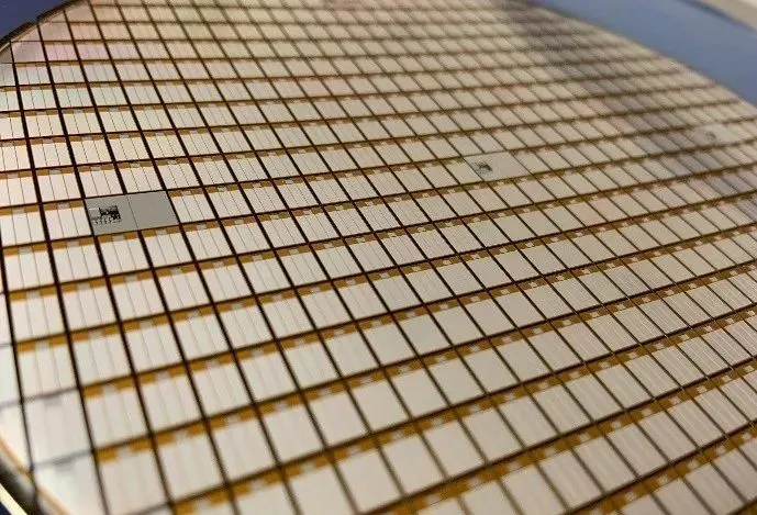 Figure 1
Zooming in on the surface of a single chip (as shown in Figure 2), its core structure typically consists of three parts: the source pad, the gate pad, and the Kelvin source pad, which is equipped on some chips. It is worth noting that not all chips contain all three types of pads; for example, some simplified designs omit the Kelvin source pad, retaining only the gate pad as the core control interface.
 Figure 2
In the edge region of the chip, there is a narrow ring structure, commonly referred to in the industry as the “voltage termination ring,” with the professional name being the edge termination ring. Currently, the mainstream design adopts a junction termination extension (JTE) structure. If we compare the chip to a “factory” for power control, then the voltage termination ring is the “protective wall” guarding the factory, the gate pad is the “control center” for transmitting commands, and the millions of switching units (Active Cells) inside the chip are the “core workshop” executing the current on-off control. Among these structures, the switching unit is often the focus of industry attention—the core performance indicators such as switching speed and conduction efficiency of the chip are largely determined by the design and manufacturing level of the switching unit. However, the roles of the gate pad and voltage termination ring are equally indispensable; the three work together to ensure that the SiC MOSFET achieves stable and efficient power control. Next, we will analyze the functions and design logic of these core structures one by one.
Voltage Termination Ring: The Device’s “Voltage Protection Shield”
The voltage termination ring surrounds the switching unit and is a key structure for the SiC MOSFET to achieve high voltage blocking capability. Currently, the vast majority of SiC MOSFETs adopt a JTE structure for the voltage termination ring design. This structure, while seemingly simple, plays multiple roles in enhancing device reliability and performance:
First, effectively suppressing leakage current and enhancing device stability. In high-voltage operating environments, small leakage currents can easily develop inside the device, and long-term accumulation may lead to performance degradation or even failure. The JTE structure, through special doping design, can effectively suppress leakage currents, significantly improving the reliability and stability of SiC MOSFETs during long-term high-voltage operation.
Second, mitigating electric field concentration and breaking through the breakdown voltage bottleneck. The breakdown voltage performance of SiC MOSFETs is related not only to the design of individual switching units but also to the optimization of the voltage termination ring. Without a voltage termination ring, the electric field at the edge of the device would be highly concentrated, causing the breakdown voltage at this point to be much lower than that of the device body, leading to premature breakdown issues. The JTE structure effectively disperses the electric field strength in the edge region through reasonable electric field distribution control, allowing the breakdown voltage of the device to approach the theoretical limit of the material itself.
Additionally, suppressing ion migration and extending device lifespan. In high-temperature and high-pressure working environments, mobile ions inside the device can drift and accumulate, causing irreversible impacts on device performance. The JTE technology can effectively block the drift paths of mobile ions by forming a deeply doped control region in the edge area of the chip; at the same time, elements such as nitrogen and boron can be introduced into the control region, which can chemically react with mobile ions, reducing their accumulation inside the device and further enhancing the reliability of SiC MOSFETs.
For the design of the JTE structure, the industry has formed a mature optimization system. Taking onsemi as an example, it has completed multiple generations of technology iterations from M1 to M3 in the SiC MOSFET field. Through continuous simulation and testing, the design and manufacturing processes of the JTE structure have reached an industry-leading level, providing a solid guarantee for the device’s high voltage resistance and high reliability.
Gate Pad and Kelvin Source Pad: The “Precise Channel” for Command Transmission
The gate pad and Kelvin source pad are the core interfaces connecting the SiC MOSFET to external driving circuits, and their design directly affects the precision and efficiency of command transmission.
The core function of the gate pad is singular yet critical—it precisely transmits the external gate drive signal to every switching unit inside the chip, achieving synchronous control of current on-off. On this basic function, some manufacturers have further enhanced the practicality of the device through integrated design; for example, onsemi’s SiC MOSFET chips integrate gate resistors. This design not only simplifies the bonding wire process during module packaging but also reduces the steps of soldering the resistor to the direct bonded copper (DBC) substrate, saving packaging space while lowering manufacturing costs and failure risks.
The Kelvin source pad is an optimized design whose core function is to enhance switching speed and reduce switching losses. Traditional source pads, while transmitting current, can cause voltage drops due to wire resistance and inductance, leading to deviations in drive signals and affecting switching performance. The Kelvin source pad adopts an independent voltage detection path, allowing for precise collection of source voltage signals, reducing drive errors, thus achieving faster switching speeds and lower losses. However, this structure requires special design when used in parallel with multiple chips to avoid performance fluctuations caused by signal interference.
Switching Unit: The “Core Workshop” for Current Control
If the voltage termination ring is the “protective wall” and the gate pad is the “control center,” then the switching unit is the “heart” of the SiC MOSFET—all current on-off operations are completed within these millions of tiny units.
From a structural perspective, all switching units are connected in parallel. The advantage of this design is that when the performance parameters of a single switching unit are fixed, the total on-resistance and short-circuit current capability of the chip can be achieved by adjusting the number of switching units: the more units, the smaller the total on-resistance and the stronger the short-circuit current carrying capacity. Currently, the switching units of SiC MOSFETs are mainly divided into planar structures and trench structures, each with its characteristics, representing different technological development paths.
SiC JTE Design: Decoding the “Performance Optimization Code” of the Voltage Termination Ring
In all structures of SiC MOSFETs, the edge termination ring (voltage termination ring) and switching unit are the two core elements determining device performance. Among them, the JTE structure of the voltage termination ring design directly relates to whether the device can achieve the expected breakdown voltage, avoiding premature failure due to edge electric field concentration. Therefore, the design of the JTE structure is a key step in the R&D process of SiC MOSFETs, requiring a comprehensive consideration of the balance and optimization of multiple parameters. The core role of SiC JTE (junction termination extension) is to improve the voltage blocking capability of SiC power devices, and its essence is to regulate the electric field distribution at the device’s edge, making the electric field strength of the entire device tend to be uniform, thereby fully utilizing the high voltage resistance characteristics of SiC materials. The following are four core factors that need to be focused on during the JTE design process:
1. Region Width and Doping Concentration: The “Basic Regulator” of Electric Field Distribution
The width and doping concentration of the JTE region are the core parameters determining the distribution pattern of the electric field at the device’s edge. Simply put, a wider JTE region can provide a larger dispersion space for the electric field, while a higher doping concentration can enhance the region’s capacity to bear the electric field. The combination of the two can effectively reduce the electric field strength at the device’s edge, thereby improving the device’s breakdown voltage. However, the optimization of width and doping concentration is not a matter of “the wider the better” or “the denser the better.” An overly wide JTE region will occupy more chip area, reducing the device’s integration level; an excessively high doping concentration may lead to impurity diffusion issues, affecting other device performances. Therefore, the design process needs to find the optimal balance between width and doping concentration through simulation and testing, enhancing breakdown voltage while considering chip integration and manufacturability.
2. Cone Angle and Depth: The “Fine Tools” for Electric Field Regulation
The cone angle (the transition angle between the JTE region and the device body) and doping depth of the JTE structure are fine parameters for further optimizing electric field distribution. A smaller cone angle allows for a smoother transition of the electric field from the device body to the edge, avoiding local electric field abrupt changes; a deeper JTE doping can make the electric field distribution in the vertical direction more uniform, reducing the risk of surface electric field concentration. The design of these two parameters requires extremely high precision in manufacturing processes. For example, controlling the cone angle relies on precise photolithography and etching processes, while doping depth needs to be achieved by strictly regulating the energy and dosage of ion implantation. Any deviation in parameters can lead to flaws in electric field distribution, subsequently affecting the device’s breakdown voltage and reliability.
3. Surface Passivation: The “Key Defense Line” for Leakage Current Suppression
The surface passivation layer is an indispensable component of the JTE structure, primarily serving to reduce leakage current on the device surface, further enhancing breakdown voltage. SiC materials have a high surface state density; without passivation treatment, leakage channels can easily form on the surface, leading to increased leakage current, and in severe cases, surface breakdown. The design of the passivation layer for SiC JTE devices needs to be optimized based on material characteristics. Common passivation methods include oxide passivation and nitride passivation, and different passivation layer materials and preparation processes can have varying impacts on the surface characteristics of the device. Designers need to conduct extensive testing to select the passivation scheme that best matches the JTE structure, ensuring long-term stability while suppressing leakage current.
4. Thermal Design: The “Performance Guarantee” in High-Temperature Environments
The high-temperature resistance of SiC materials is one of the core advantages of SiC MOSFETs, with operating temperatures far exceeding those of traditional silicon-based devices. However, high-temperature environments can also impact the performance of the JTE structure—long-term high temperatures may lead to impurity diffusion in the doping region and aging of the passivation layer, thereby reducing device reliability. Therefore, thermal design is an essential aspect of JTE structure design. The thermal design of JTE mainly focuses on heat dissipation and thermal stress relief. For example, in the layout design of the JTE region, compatibility with the chip’s heat dissipation structure needs to be considered to ensure that heat can be quickly conducted away; in material selection, highly thermally stable doping elements and passivation materials should be chosen to minimize performance degradation at high temperatures. Additionally, simulations should be conducted to predict potential issues caused by thermal stress under different temperature conditions and to avoid them in the design. Overall, the design of SiC JTE is a complex process of multi-parameter trade-offs. From width and doping concentration to cone angle and depth, and then to surface passivation and thermal design, each link requires precise optimization and simulation. Only by organically combining these parameters can the expected breakdown voltage and reliability be achieved, laying the foundation for the high performance of SiC MOSFETs.
Switching Unit: The “Performance Core Engine” of SiC MOSFETs
If the JTE structure determines the “voltage ceiling” of SiC MOSFETs, then the switching unit determines the “efficiency floor” of the device. As the core execution unit for current on-off operations, the structural design, density, and process level of the switching unit directly affect key performance indicators such as chip on-resistance and switching speed.
1. The Two Mainstream Structures: The “Path Competition” of Planar and Trench
According to the differences in gate structure, MOSFETs (including silicon-based and silicon carbide-based) can be divided into two main categories: planar structures and trench structures, as illustrated in Figure 3. From a basic structural perspective, the principles of planar/trench structures for silicon-based and silicon carbide-based MOSFETs are similar, but due to the significant differences in crystal structure and chemical properties between SiC and silicon materials, their manufacturing processes and design focuses are entirely different. For example, SiC materials have higher chemical stability, making traditional wet etching difficult to achieve precise processing; therefore, dry etching processes are widely used in the manufacturing of SiC MOSFETs. Additionally, the atomic bond energy of SiC is stronger, requiring ion implantation to be conducted at higher temperatures, and the doping elements (such as nitrogen and aluminum) also differ significantly from those in silicon-based devices. These material property differences directly lead to the uniqueness of the design and manufacturing of SiC MOSFET switching units.
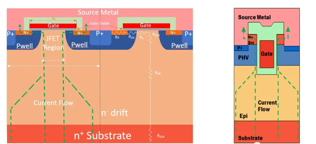 Figure 3
From the current market application perspective, the vast majority of SiC MOSFETs internationally adopt planar structures, with only a few manufacturers offering trench structure products. From a technological development trend perspective, trench structures are considered an important development direction for the future due to their higher unit density and lower on-resistance potential. However, at present, the potential of planar structures has not been fully tapped, while trench structures are limited by the complexity of manufacturing processes and have not fully realized their theoretical performance advantages. To objectively measure the performance of different structural switching units, the industry has introduced a key indicator—specific on-resistance Rsp (Rdson * Area), which represents the on-resistance value corresponding to unit chip area. A lower Rsp value means that the device has lower on-resistance and lower conduction losses for the same chip area. This indicator provides a unified performance comparison benchmark for SiC MOSFETs of different structures and sizes. Planar SiC MOSFETs have two significant advantages: first, high reliability, as the gate oxide layer of planar structures experiences more uniform stress, making it less prone to breakdown issues caused by local electric field concentration; second, the design and processing are relatively simple, making it easier to achieve large-scale production and yield improvement. Based on these advantages, planar structures remain the mainstream choice for SiC MOSFETs, especially in fields with high reliability requirements such as new energy vehicles and industrial control.
2. Optimization Directions for Planar Structures: From “Density Improvement” to “Resistance Reduction”
For planar SiC MOSFETs, the core of switching unit design optimization revolves around “reducing the Rsp value,” mainly achieved through three directions: reducing the spacing between switching units (i.e., pitch value), increasing unit density, and optimizing the reliability of the gate oxide layer. The spacing between switching units (pitch value) is closely related to the gate width (Wg)—as the pitch value decreases, the gate width typically also shrinks. This change not only increases unit density but also has positive implications for gate reliability. The gate oxide layer of SiC MOSFETs is extremely thin, usually less than 100 nanometers, and such a thin oxide layer demands extremely high processing precision. Dry etching processes, with their excellent processing precision, have become the core technology for preparing gate oxide layers, effectively controlling the thickness and uniformity of the oxide layer and avoiding gate failures caused by processing errors. To understand the impact of switching unit optimization on the Rsp value, it is first necessary to clarify the composition of on-resistance. According to the on-resistance model of SiC MOSFETs (as shown in Figure 3A), the total on-resistance Rdson consists of multiple parts, specifically expressed as: Rdson = Rs + Rch + Ra + Rjfet + Rdrif + Rsub. Among these, the channel resistance Rch and accumulation layer resistance Ra are the main components, accounting for over 60%, thus becoming the core targets for on-resistance optimization. Reducing the spacing between switching units (pitch value) can increase the number of switching units per unit area, thereby increasing the total channel width and reducing channel resistance Rch. At the same time, optimizing unit structure design, such as adjusting doping concentration and distribution, can effectively reduce accumulation layer resistance Ra, further decreasing total on-resistance. However, the optimization of switching units is not simply about making everything smaller. When the gate width (Wg) is reduced to a certain range, a “reverse effect” may occur—where the gate resistance increases, leading to a rise in the Rsp value. Therefore, the design of switching units needs to comprehensively consider the interrelationships between pitch value, Wg, doping concentration, and other parameters, finding the best combination through extensive simulations and tests. Onsemi has accumulated rich experience in optimizing planar SiC MOSFETs through multiple generations of technology iterations. In the process of upgrading from the M1 to M3 series, it has achieved a significant reduction in Rsp values through continuous optimization of switching unit layout and process parameters, while also reaching industry-leading levels in device performance, mass production yield, and reliability. From the cross-sectional view of the chip (as shown in Figure 4), the layout characteristics of the switching units can be more intuitively seen—using a strip structure, the switching units are closely arranged, forming a massive current path in parallel. This layout method ensures that current is evenly distributed within the chip, avoiding overheating and failure issues caused by excessively high local current density, further enhancing the reliability and lifespan of the device.
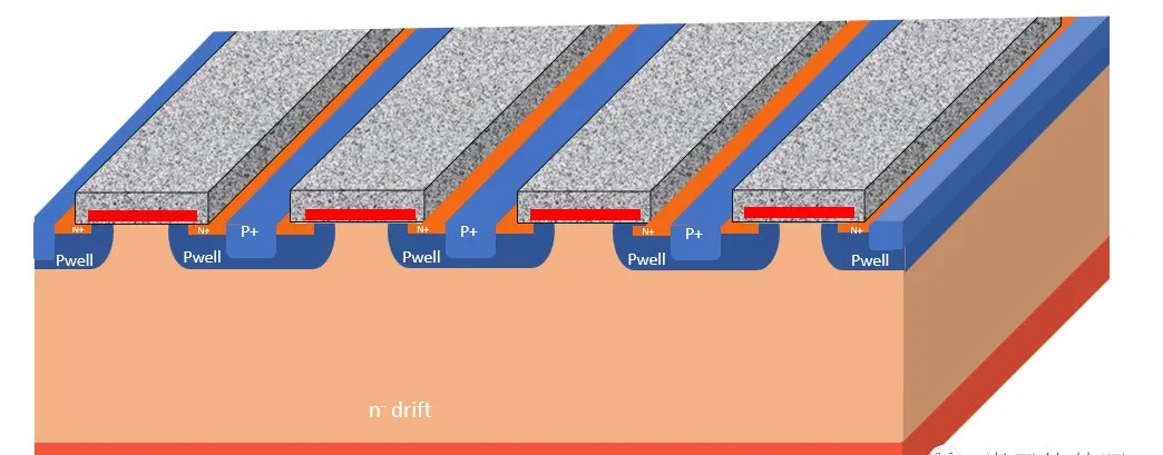 Figure 4
3. Core Considerations for Rdson Design: The Art of Balancing Multiple Parameters
On-resistance Rdson is one of the core performance indicators of SiC MOSFETs, and its design optimization is a complex process involving the mutual balancing of multiple parameters. In addition to the structure and density of the switching unit, the following three factors also significantly impact the Rdson value:
(1) Channel Width and Doping Concentration
The channel width and doping concentration of the switching unit directly determine the current conduction capability. A wider channel can provide a larger flow path for current, while a higher doping concentration can reduce the resistance value of the channel. The combination of the two can effectively lower Rdson and enhance the device’s current carrying capacity. However, the increase in doping concentration is not without limits—excessively high doping concentrations may lead to a decrease in the device’s breakdown voltage, affecting its high-voltage operating capability. Therefore, the design of channel doping concentration needs to find a balance between “low Rdson” and “high breakdown voltage,” optimizing based on the target application scenarios of the device (such as low-voltage industrial power supplies or high-voltage new energy vehicle inverters).
(2) Gate Oxide Layer Thickness
The thickness of the gate oxide layer is a “double-edged sword” parameter: a thinner oxide layer can reduce gate capacitance and enhance the switching speed of the device, but it also increases gate leakage current and raises the risk of oxide breakdown; conversely, a thicker oxide layer can improve gate reliability but may lead to slower switching speeds. Therefore, the design of gate oxide layer thickness needs to be balanced according to the application requirements of the device. For example, SiC MOSFETs used in high-frequency power supplies need to prioritize switching speed, allowing for a thinner oxide layer while enhancing reliability through optimized passivation processes; whereas devices used in high-voltage, high-reliability scenarios need to prioritize gate stability, opting for a slightly thicker oxide layer design.
(3) Gate Design
The structural design of the gate directly affects the size of the gate resistance, which in turn has an indirect impact on Rdson and switching speed. A lower gate resistance can accelerate the transmission speed of gate signals, enhancing the switching efficiency of the device, but it may also increase gate capacitance, leading to higher switching losses. The core of gate design is to achieve a balance between “low resistance” and “low capacitance.” For example, optimizing the materials and thickness of the gate metallization layer can reduce gate resistance; adjusting the overlap area between the gate and source/drain can control the size of gate capacitance. These design detail optimizations require support from precise simulation tools and extensive experimental data to achieve optimal performance. In summary, the Rdson design of SiC MOSFETs is a system engineering task involving the collaborative optimization of multiple aspects such as channel structure, doping processes, and oxide layer preparation. Designers need to conduct repeated simulations, tests, and validations to comprehensively balance various performance indicators to create products that meet application needs and possess market competitiveness.
Integrated On-Chip Gate Resistor: The “Detail Innovation” that Enhances Module Value
In the design of SiC MOSFETs, in addition to the core switching unit and voltage termination ring, some “detail innovations” can also bring significant value enhancements to the device, with integrated on-chip gate resistors being a typical example (as shown in Figure 5). This design, while not directly altering the core performance parameters of the device, can greatly optimize the design and manufacturing processes of the module, bringing numerous conveniences to downstream applications.
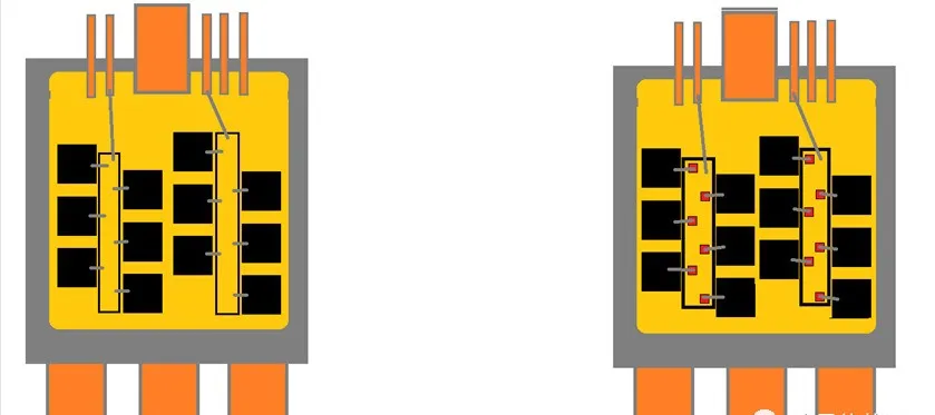 Figure 5
In traditional SiC MOSFET module designs, the gate resistor needs to be soldered as an independent component to the direct bonded copper (DBC) substrate, and then connected to the gate pad of the chip through bonding wires. This process not only increases the manufacturing steps of the module but may also lead to increased contact resistance due to bonding wire process errors, affecting the precision of gate signal transmission. The design of integrated on-chip gate resistors fundamentally solves these problems, with advantages mainly reflected in the following four aspects:
1. Simplifying Manufacturing Processes and Reducing Failure Risks
By integrating the gate resistor on-chip, the module manufacturing process can directly eliminate the soldering and bonding wire connection steps for independent gate resistors, simplifying the process flow. At the same time, reducing the number of solder joints and bonding wires can effectively lower the risk of module failures caused by solder defects and bonding wire disconnections, enhancing the manufacturing yield and reliability of the module.
2. Reducing Process Steps and Controlling Production Costs
The procurement, storage, and soldering processes of independent gate resistors all increase the BOM cost and manufacturing cost of the module. The design of integrated on-chip gate resistors eliminates the procurement costs of independent resistors while reducing the investment in soldering equipment and labor costs, effectively controlling the overall cost of the module. For large-scale application scenarios such as new energy vehicles, the economic benefits brought by this cost optimization are particularly significant.
3. Supporting Miniaturization of Packaging and Enhancing Power Density
In power module design, space resources are often very tight. Independent gate resistors and their connection structures occupy a certain amount of packaging space, limiting the improvement of module power density. Integrated on-chip gate resistors merge the resistor with the chip, eliminating the need for additional installation space, thus enabling miniaturization of the module design. The reduction in module size not only decreases the spatial occupation of application devices but also enhances power density, aligning with the development trend of “miniaturization and lightweight” in power electronic devices.
4. Optimizing Signal Transmission and Enhancing Control Precision
Binding wires between independent gate resistors and the chip introduce additional parasitic inductance and resistance, which may lead to delays or distortions in gate drive signals, affecting the switching performance of the device. Integrated on-chip gate resistors connect directly to the gate pad, minimizing the signal transmission path and reducing the impact of parasitic parameters, allowing gate signals to be transmitted more accurately and quickly to the switching unit, enhancing the control precision and switching efficiency of the device. Onsemi has adopted the design of integrated gate resistors in its M3 series SiC MOSFETs. This detail innovation not only enhances the market competitiveness of the product but also provides downstream module manufacturers with a more convenient and efficient solution. For example, its M3E series 1200V SiC MOSFET bare chip, with integrated design and optimized JTE structure, achieves lower conduction losses and higher power density in new energy vehicle traction inverters, helping the entire vehicle improve energy utilization efficiency and range; while the M3S series 650V planar SiC MOSFET achieves excellent switching performance and efficiency in UPS, energy storage, and other high-frequency applications through integrated design and Kelvin source configuration.
The Logic of “Power Revolution” in Tiny Chips
From the foundational preparation of substrates and epitaxial wafers to the structural design of voltage termination rings, switching units, and pads, and then to the detail optimization of integrated gate resistors, every technical link in SiC MOSFETs embodies the core logic of “precise control” and “balanced optimization.” High-quality substrates and epitaxial wafers are the “cornerstone” of device manufacturing, but what truly determines the performance limits of the device is the technical accumulation and innovation capabilities that run through the entire design and manufacturing process. The JTE structure design of the voltage termination ring, through precise regulation of electric field distribution, builds a “voltage protection shield” for the device, achieving a unity of high voltage resistance and high reliability; the structural optimization and process upgrades of the switching unit create the “performance core engine” of the device by increasing unit density and reducing on-resistance, driving continuous breakthroughs in switching efficiency and power density; while detail innovations such as integrated on-chip gate resistors provide more convenient and efficient solutions for module manufacturing from the perspective of application needs, accelerating the industrial application process of SiC MOSFETs. Driven by emerging industries such as new energy vehicles, photovoltaics, and energy storage, the market demand for SiC MOSFETs continues to grow, and the requirements for device performance are constantly increasing. The technological iterations from onsemi’s M1 to M3 series demonstrate that the development trend of SiC MOSFETs is “more efficient, more reliable, and more economical”—achieving lower losses and higher voltage resistance through optimization of JTE structures and switching unit designs; ensuring long-term reliability of devices in extreme environments by enhancing manufacturing process precision; and reducing application costs through integrated and miniaturized designs, promoting the widespread adoption of SiC technology in more fields. Between tiny chips lies the revolutionary wave of power electronics technology. With continuous innovation in design concepts and ongoing advancements in manufacturing processes, SiC MOSFETs will play an increasingly important role in the future energy revolution, providing core support for efficient energy conversion and utilization. For industry practitioners, deeply understanding the design logic and technical details of SiC MOSFETs not only helps grasp technological development trends but also provides a solid theoretical foundation for product innovation and application implementation.
Source:Qixin SemiconductorStatement: We respect originality,and also focus on sharing; the text and images copyright belong to the original author. The purpose of reprinting is to share more information and does not represent the position of this account. If your rights are infringed, please contact us in a timely manner, and we will delete it as soon as possible. Thank you!!
/ END /