
This article analyzes the strategic significance of third-generation semiconductors and discusses the development status of China’s technology and industrial capacity in related fields. It explains that “large size and cost reduction” are the current focus of silicon carbide (SiC) and gallium nitride (GaN) technology development, and explores the development models of third-generation semiconductor companies as well as potential problems and risks. Although China has a solid foundation, there are still shortcomings. It is suggested that under national policy guidance, development should be driven by applications, increasing continuous support for production lines, systematically enriching product forms, promoting high-quality development of the third-generation semiconductor industry, and seizing new opportunities for future applications.
In the early 1980s, third-generation semiconductors began to emerge, achieving significant breakthroughs in the field of compound lighting, and have now formed a trillion-level market globally. In the past three years, the development of third-generation semiconductors has slowed due to the COVID-19 pandemic, but the global scale is still increasing at an annual compound growth rate of about 10%. With the emergence of innovative technologies such as deep ultraviolet light-emitting diodes (LEDs), Mini-LED, and Micro-LED, third-generation semiconductors are opening up new application scenarios in optoelectronics, such as new displays, smart agriculture, and healthcare, further expanding the market scale.
In 1993, the first gallium nitride (GaN) high electron mobility transistor (HEMT) device with microwave characteristics was publicly reported, rapidly advancing the research and application of third-generation semiconductors in microwave RF, especially GaN RF devices, which, due to their unique characteristics of high power, high efficiency, high linearity, high operating voltage, and radiation resistance, have become ideal substitutes for silicon (Si) and gallium arsenide (GaAs) devices. They play important roles in military equipment, aerospace, and fifth-generation mobile communication (5G) technologies, showcasing broad development prospects.
In the early 21st century, the United States was the first to apply silicon carbide (SiC) to equipment using S-band solid-state microwave RF devices. Although it was gradually replaced by GaN, its high voltage and high frequency characteristics have gained favor in the power electronics field, gradually becoming a substitute for Si power electronic devices. Especially after 2002, SiC single crystal substrate technology developed rapidly, significantly reducing manufacturing costs, and is expected to play a major role in new energy vehicles, high-speed rail, and smart grids, supporting a market scale of over 10 trillion yuan.
The third-generation semiconductors have experienced over 20 years of development in optoelectronics, RF electronics, and power electronics, supporting a trillion-level market scale, and continue to emerge with new application scenarios, stimulating new development potential.
Massive Application Scenarios in the Market
5G Demonstrates “China Speed,” with Vast Space for GaN RF Devices
5G is currently a representative and leading network information technology, characterized by high speed, ubiquitous networks, low power consumption, low latency, and high reliability. It will achieve ubiquitous interconnection of all things and deep human-machine interaction, penetrating various industries and fields of the economy and society, becoming a key new infrastructure supporting the digital, networked, and intelligent transformation of the economy and society.
5G base stations place higher demands on RF devices; traditional laterally diffused metal oxide semiconductors (LDMOS) cannot meet the high frequency requirements of 5G, while GaN can adapt to frequency ranges extending to 40GHz or even higher, meeting the high-frequency needs of 5G; GaN has soft compression characteristics, making it easier to pre-distort and linearize for higher efficiency; GaN can achieve higher power density, reaching about four times the power density of LDMOS devices; and GaN packaging sizes are only 1/4 to 1/7 of LDMOS, making GaN RF devices more suitable for 5G base stations. In 2010, GaN-based high-power microwave amplifying devices were first applied in high-end base station equipment with small volume and high linearity, beginning to enter the mobile communication market. With the comprehensive rollout of fourth-generation mobile communication (4G) wireless network infrastructure, the application of GaN has significantly increased. The market share of Si-based LDMOS devices above 2GHz has dropped from 92% to 76%. The introduction of 5G has further increased the acceptance of GaN microwave power amplifiers, which can only rely on GaN-based HEMT devices in high-frequency bands. Currently, GaN-based HEMT microwave RF technology has basically achieved a significant leap for third-generation semiconductors compared to previous generations of semiconductors (Si-based LDMOS, GaAs/InP-based pHEMT, etc.).
As the 5G construction process unfolds, China’s 5G frequency bands have gradually expanded from the initial 4.9, 3.5, and 2.6GHz to 2.1GHz, 700MHz, and the latest 900MHz.Base station structures have transitioned from large-scale dense massive multiple-input multiple-output (MIMO) antenna arrays back to traditional MIMO structures, and the number of receiving and transmitting channels has decreased from the original 64, 32 channels to 8, 4 channels.At the same time, new demands have been placed on GaN RF devices, requiring the output power of devices to increase from the original 100W level to 500-700W or even higher.The changes in frequency, channel count, and power require innovation and research and development from materials, design, processes, and packaging to meet the new base station development and production demands.
According to a report released by the Ministry of Industry and Information Technology of the People’s Republic of China (MIIT), by the end of May 2023, the number of 5G base stations in China had reached 2.844 million, with over 2.05 billion mobile IoT terminal users.China is the first country in the world to establish a 5G SA (standalone networking) network, maximizing the end-to-end network slicing, massive connections, and ultra-reliable 5G characteristics.As the first of the new infrastructure, investments from 2019 to 2022 have increased year by year to 401.6 billion yuan.By 2025, cumulative investment in China’s 5G network construction is expected to reach 1.2 trillion yuan, driving related investments of over 3.5 trillion yuan.Based on the development characteristics of mobile communications every ten years, 5G development has progressed from shallow to deep, and 5G technology continues to evolve, with 5.5G expected to enter the commercial stage in 2024.The new standards will achieve the ultimate goal of capability enhancement, boundary extension, and efficiency improvement through the construction of six core pillars: spectrum utilization, native artificial intelligence, uplink enhancement, industry focus, intelligent management, and green low-carbon initiatives, promoting comprehensive penetration of 5G industry applications.With the saturation of low-frequency applications and the demand for wider bandwidth and greater communication capacity, 5G communication will inevitably evolve toward millimeter-wave frequencies, and 6G mobile communication may even increase frequencies to terahertz.Traditional RF device product forms can no longer meet new requirements, necessitating the development of millimeter-wave single-chip integrated power amplifier chips, integrating amplification, switching, and low-noise amplification into multifunctional chips.GaN terahertz devices have advantages in the terahertz field due to their larger effective electron mass, higher longitudinal phonon energy, faster intersubband electron scattering, greater negative resistance area current peak-to-valley ratio, and higher two-dimensional electron gas density.Of course, when frequencies enter the terahertz band, traditional transmit-receive modules using thick film processes will not meet the requirements for base station miniaturization, high efficiency, and high integration. Innovative research and development of three-dimensional packaging techniques using microelectronic processes will be necessary to achieve a transition from traditional two-dimensional integration to three-dimensional integration, evolving multifunctional packaging devices that integrate antennas, transmission and reception, control, and analog-to-digital conversion functions, reducing the volume and mass of devices by more than an order of magnitude while enhancing functionality by more than an order of magnitude.
The “Dual Carbon” Strategy Accelerates New Applications for SiC Power Electronic Devices
In September 2020, China clearly proposed the goal of “carbon peak” by 2030 and “carbon neutrality” by 2060.Third-generation semiconductors are known as green semiconductors, and SiC power electronic devices possess characteristics such as high breakdown voltage, high efficiency, and high frequency, making them core devices that support the “dual carbon” strategy.The chips made from them have broad application prospects in new energy vehicles, photovoltaic inverters, rail transit, and smart grids.
In the field of new energy vehicles, low-voltage DC/DC conversion requires Schottky barrier diode (SBD) devices rated at 650V and below;onboard chargers (OBC) require SiC MOSFETs rated below 1700V, with conduction resistance levels of 25, 40, 80, and 160mΩ;in the main drive, voltage requires 1200V with conduction resistance less than 15mΩ, and current above 100A, with chip development power levels for power modules at 400, 600, and 800A to meet different endurance requirements.At the same time, high-voltage architecture is essential for achieving high-power fast charging. With the popularization of 800V fast charging systems, new SiC power electronic device products need to be developed to meet the changing requirements for voltage, current, and conduction resistance, evolving towards higher voltage, larger current, and smaller conduction resistance in new energy vehicle applications.Using SiC power devices can improve the energy utilization of batteries due to their high energy conversion efficiency.For example, in systems equipped with 1200V SiC MOSFETs, inverter energy consumption can be reduced by more than 60%, while also lowering overall vehicle energy consumption, achieving a reduced battery capacity requirement.Additionally, due to their high power density and frequency, SiC devices can reduce the size and mass of power conversion modules. Their stronger tolerance to high temperatures also saves on heat dissipation components, achieving vehicle lightweighting.For instance, a bidirectional OBC using all-SiC MOSFETs can achieve more than double the switching frequency compared to Si solutions, while also reducing the number of power devices and gate drivers by over 30%, enhancing system lightweighting and overall operational efficiency.Overall, new energy vehicles driven by SiC power devices can significantly reduce energy losses, increasing the endurance range by 5% to 10% under the same battery capacity.The “Carbon Peak Implementation Plan in the Industrial Sector” issued by the MIIT states that by 2030, the proportion of new energy and clean energy-powered vehicles will reach about 40%, providing a broad market for the application development of SiC power electronic devices.
In the rail transit field, both domestic and international attention has focused on the application research of SiC devices in traction converter systems, with some institutions already commercializing products and installing them in rail vehicles. Mitsubishi Electric has developed a 3.3kV all-SiC power module suitable for rail traction systems; by applying this high-voltage all-SiC power module in the main circuit system of rail vehicle inverter systems, the main circuit system can save about 30% of power compared to existing systems. Recently, SiC has made further progress in the rail transit field, with the Chengdu Metro and Xi’an Metro applying SiC-based converters and permanent magnet synchronous motor traction systems. Currently, China’s urban rail transit operating lines have surpassed 10,000 km, and the corresponding mileage by the end of the 14th Five-Year Plan is expected to reach 15,000 km, with the national railway operating mileage reaching 165,000 km, including 50,000 km of high-speed rail. This scenario highlights the advantages of medium-voltage SiC power electronic devices, which will gradually replace Si-based power electronic devices, representing a medium-term market demand.
In the green energy sector, the direct current generated by photovoltaic power generation must be inverted into alternating current to be integrated into the grid, a process that requires the participation of power devices. Compared to Si-based IGBTs, SiC power modules can reduce switching losses by 85%, directly improving the efficiency of electrical energy conversion. According to estimates by the International Energy Agency (IEA), if only 2% of distributed solar photovoltaic systems deploy SiC by 2024, the additional generated electricity could reach up to 10GW. China is a major consumer of electrical energy, with total electricity consumption in 2022 reaching approximately 8.6 trillion kilowatt-hours. The demand for smart grids requires third-generation semiconductor power electronic devices rated at tens of thousands of volts and thousands of amps, with commercial use planned by 2035, presenting a broader market demand than new energy vehicles. The breakdown voltage and current requirements for SiC power electronic devices in this scenario are more than ten times those of new energy vehicle devices, indicating essential differences in R&D and production. Innovation and research and development are also required in materials, design, processes, and packaging, reflecting the long-term market demand for SiC power electronic devices.
Military Demand Accelerates the R&D and Application of New Technologies
Globally, military equipment’s demand for new materials, new devices, and new processes is a significant driving force for the development of the semiconductor field.Third-generation semiconductors are key cores supporting national defense construction and are crucial elements for mastering the initiative in future warfare.The excellent performance of third-generation semiconductors can significantly reduce the size of radar, communication equipment, and guidance systems.At the same time, they can greatly enhance combat effectiveness, playing an extremely important supporting role in improving the level of unmanned, intelligent, and informationized equipment, making it a focus of competition in national defense technology among various countries.For instance, after adopting third-generation semiconductor devices, radar can significantly enhance detection range and accuracy without increasing size and weight, enabling the discovery and locking of stealth targets;through massive combined power, it can directly burn out enemy electronic devices, achieving hard-kill electronic countermeasures;special operations teams can achieve secure communication under radio silence conditions.The United States widely uses third-generation semiconductors in next-generation electronic jammers, long-range identification radars, guided missiles, and all-electric ship integrated power systems.
In fact, the initial industrial foundation development plans of major countries globally have shown clear military tendencies and application demands. Currently, GaN-based HEMT microwave RF technology has largely achieved significant leaps compared to previous generations of semiconductors. Major global manufacturers layout GaN-based semiconductor RF devices include the United States’ Cree (now Wolfspeed), Qorvo, MACOM, and Raytheon, as well as Germany’s Infineon, Canada’s GaN Systems, Japan’s Mitsubishi Electric, and the Netherlands’ NXP. In terms of manufacturing maturity, GaN products from the United States’ Raytheon and Qorvo have reached the highest levels of manufacturing maturity assessment by their Department of Defense, and the manufacturing processes of GaN RF devices have met the best performance, cost, and capacity targets and are capable of supporting full-rate production. In 2014, Raytheon announced the deployment of GaN modules in the “Patriot” air defense system; in 2021, it licensed its GaN-on-Si technology to GlobalFoundries to jointly develop IC processes capable of handling 5G and 6G millimeter-wave signals, elevating the scale production level of GaN-based RF devices to a new level and further compressing RF costs.
With new working scenarios, demands for new forms of products such as reconfigurable multifunctional amplifiers, microwave and millimeter-wave multifunctional circuits integrating different functions, transceiver components, digital transceiver components, terahertz chips, three-dimensional integrated multifunctional devices, ultra-high power devices, and heterogeneous integrated devices are continuously emerging, promoting the exploration and innovative R&D and industrialization of new technologies and products in the third-generation semiconductor field. New application scenarios are constantly emerging in the third-generation semiconductor field, and new standards are being established, leading to new demands for third-generation semiconductor devices. Traditional single-function devices will be replaced by integrated devices that are high-frequency, high-power, multifunctional, highly integrated, and miniaturized, which will continue to support the development of emerging industries and the trillion-level market for at least the next 10 to 15 years.
Continuous Emergence of Technological Achievements, Sustained Improvement in Industrialization Level
Through continuous support from national policies and relevant ministries, China’s third-generation semiconductor technology has made continuous breakthroughs during the 12th and 13th Five-Year Plans, achieving significant progress in basic scientific issues and acquiring a series of core intellectual property rights, laying the foundation for the development of China’s third-generation semiconductor industry and cultivating a group of research talents and innovative teams. The “14th Five-Year Plan” national key R&D program (2021-2023) guidelines have been published, continuing to include third-generation semiconductors as a key special project in “new displays and strategic electronic materials” for focused support (Table 1), continuously addressing issues of usability and sustainable innovation capability, and promoting a sustained improvement in industrialization levels.
Table 1: Guidelines for Soliciting Opinions on the 14th Five-Year Plan Key Special Project for “New Displays and Strategic Electronic Materials” Third-generation Semiconductor Direction 2021-2023
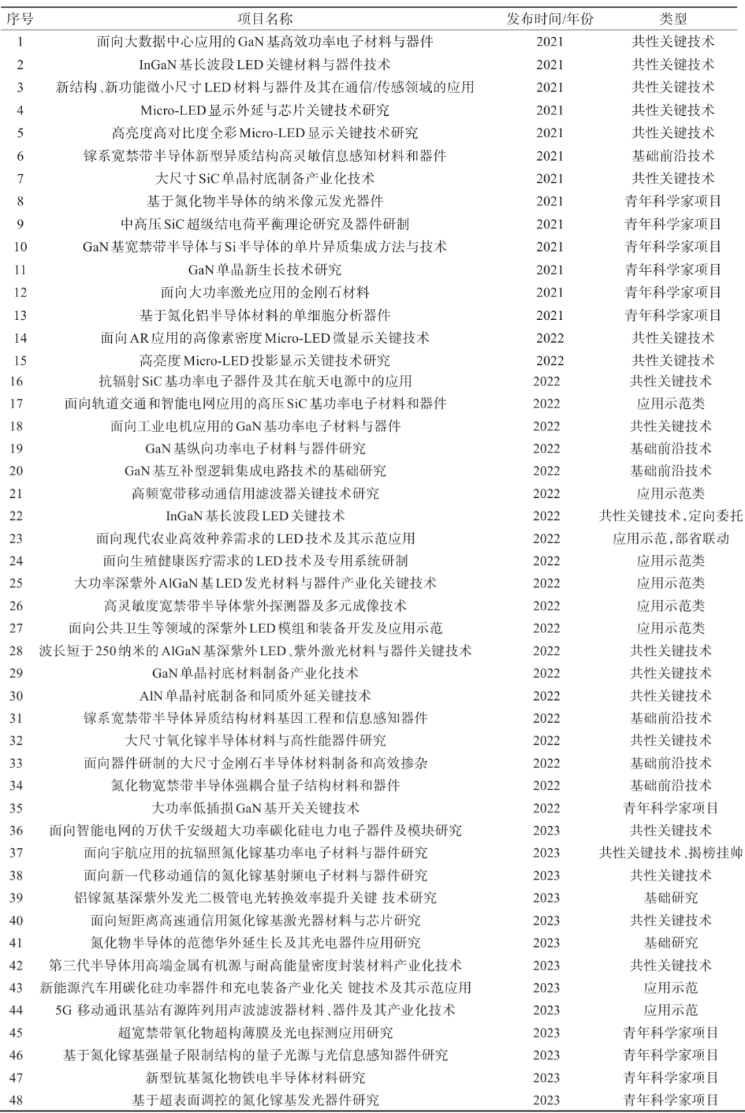
China’s GaN industry is forming a trend of midstream enterprises extending to upstream and downstream, achieving full coverage in RF, LED, and power electronic devices. In recent years, projects in the GaN field have emerged one after another. Particularly in the substrate field, breakthroughs have been made in n-type doping and compensation doping for GaN single crystal material growth, developing high conductivity and semi-insulating GaN single crystals. Four-inch (1 inch = 2.54 cm) GaN substrate products reach a thickness of (650±50) μm, with defect density <3×106 cm-2; four-inch iron-doped GaN substrate products can reach a thickness of (420±50) μm, with defect density <5×106 cm-2; at the same time, the first global breakthrough of GaN crystals exceeding 1 cm in thickness has been achieved. In terms of GaN RF devices, China has formed a series of GaN microwave power devices and monolithic microwave integrated circuit (MMIC) products, with operating frequencies reaching the W band and maximum output power exceeding 500W. The development of multifunctional integrated chips for transceivers is a hot research area, having reached international advanced levels.In terms of GaN power electronic devices, domestic companies have launched low-voltage ultra-low conduction resistance and high-voltage GaN power device products rated at 650-700V.At the application end, the development of the domestic GaN power component market is mainly driven by consumer electronics, with key applications including fast chargers, audio, wireless charging, power supplies, and other consumer-grade product applications.As the technology for GaN power electronic devices matures, it is also beginning to penetrate into new energy vehicles and industrial applications.
In the SiC field, a complete industrial chain has formed domestically, covering equipment, materials, devices, and applications. In terms of domestic equipment, comprehensive capabilities across all process segments, including crystal growth, material processing, epitaxial growth, high-temperature injection, packaging assembly, and testing, have been established, involving the R&D and industrialization of core equipment in each link of the chain. Currently, substrate materials have transitioned from 4-inch to 6-inch SiC substrates, and 8-inch SiC substrates have been developed for small batch supply. Shandong Tianyue Advanced Technology Co., Ltd. has made breakthroughs in the preparation of high-quality low-defect 8-inch crystals using liquid phase methods; 6-inch SiC epitaxial wafers cover materials for 600-1700V SiC power electronic devices, with 8-inch epitaxial products rolling off the production line. In the device segment, domestic manufacturers are strengthening the technical R&D and production line investment of SiC devices to accelerate domestic substitution. In terms of SiC MOSFETs, companies such as China Electronics Technology Group Corporation (CETC), Sanan Optoelectronics Co., Ltd., and Yangzhou Yangjie Electronic Technology Co., Ltd. have developed 1200V series products with excellent characteristics such as conduction resistance, with some already in vehicle installations. In terms of SiC diodes, manufacturers such as Sanan Optoelectronics, China Resources Microelectronics Co., Ltd., and Wingtech Technology Co., Ltd. have developed SiC diodes with outstanding performance data, mainly applied in ultra-high performance, low loss, and high-efficiency power supply fields. At the terminal application level, new energy vehicles account for the largest share, with multiple brands and types of new energy vehicles continuously adopting SiC solutions, and 800V is set to become the mainstream platform for electric vehicles.
“Large Size, Low Cost” Becomes the Development Focus, Accelerating Capacity Layout
Affordable products are an eternal goal for industrial development, and expanding wafer sizes is one of the most effective ways. The third-generation semiconductor industrial chain exhibits significant upstream traction effects, where substrate, epitaxy, and device manufacturing are key links distinguishing it from traditional semiconductor production, with substrate and epitaxy production accounting for over 60% of costs. Currently, China’s GaN RF device product R&D and production mainly utilize a 4-inch wafer system, while SiC power electronic device products are in the product introduction and small batch application stage, with the mainstream domestic SiC substrate, epitaxy, and production lines being 6-inch systems.According to estimates by BAE Systems, if GaN RF devices transition from 4-inch wafer production to 6-inch wafer production, the cost per square millimeter will drop from $3 to $1.5.Moreover, mature 8-inch SiC technology will effectively address the limited yield and excessive edge waste of 6-inch SiC wafer chips, reducing unit chip costs by 30% to 50%.
In terms of GaN substrates, the upstream raw materials in the industrial chain include GaN substrates and GaN epitaxial wafers, which have high raw material costs. For instance, GaN-on-Si wafers can produce 80% to 90% more devices per 8-inch wafer compared to 6-inch wafers, directly impacting device costs. Chinese companies are performing well in this regard, with Innoscience becoming the world’s largest mass production enterprise for 8-inch Si-based GaN. However, GaN-on-SiC is mainly constrained by the size limitations of semi-insulating SiC wafer substrates. In the substrate field, GaN substrates still face certain technical difficulties, with an international market price of up to $3000 to $5000 for a 2-inch GaN wafer, and quantities are very limited. As such, most manufacturers use SiC or sapphire as substrate materials for GaN. While this approach simplifies the substrate processing and lowers costs, it is prone to defects such as cracks and warping. Currently, the quality and yield of GaN epitaxial wafers almost determine the performance and yield of device products, and the cost of epitaxial wafers also accounts for nearly 50% of the entire GaN value chain. Around 2015, many foreign companies and research institutions produced 2-inch self-supporting GaN substrates with millimeter thickness and achieved mass production, with reports of 4- to 6-inch GaN substrate technologies as well. Companies like Sumitomo Chemical have achieved the homoepitaxial growth of low-dislocation-density GaN single crystal substrates of <105 cm-2. Sciocs has successfully produced 6-inch GaN substrate prototypes and is rapidly establishing mass production technology, aiming to triple GaN single crystal substrate sales within ten years. Domestic companies are also continuously increasing their GaN substrate research and production capabilities, gradually achieving successful development of 1, 2, 4, and 6-inch GaN single crystal materials since 2021.
In terms of SiC wafer substrates, there is a continuous evolution towards larger sizes, where larger substrate sizes allow for more chips to be manufactured per substrate, thereby lowering unit chip costs. In 2015, Wolfspeed showcased 8-inch SiC samples; in 2019, it completed the first batch of 8-inch SiC wafer samples; by April 2022, it became the world’s first to officially use an 8-inch SiC wafer factory, achieving shipments in the first quarter of 2023. Meanwhile, Wolfspeed has invested billions of dollars to expand its existing U.S. factory and establish a new 8-inch SiC production line in Germany. Other major international manufacturers, such as Coherent, also showcased 8-inch conductive SiC substrates in 2015 and launched semi-insulating 8-inch SiC substrates in 2019, planning to achieve mass production by 2024 and increase production capacity by 5 to 10 times, including 8-inch substrates, by 2025. Infineon announced in September 2020 that its 8-inch SiC wafer production line had been completed, achieving mass production in 2023 and planning to achieve mass production of 8-inch SiC substrate devices by 2025, significantly expanding its Malaysian factory to become the world’s largest 8-inch SiC wafer factory. Several companies, including ST and ROHM, have also raised their 8-inch SiC mass production plans to 2023, subsequently investing heavily in new large-scale facilities. Currently, Wolfspeed is the only company in the world capable of mass-producing 8-inch SiC wafers, while most other international companies have set their mass production nodes around 2023. In the next 2 to 3 years, Wolfspeed’s 8-inch SiC production capacity will maintain its dominant position until more companies increase their production capacity.
Many domestic manufacturers are also entering the 8-inch SiC tier. In 2020, Shanxi ShuoKe Crystal Co., Ltd. successfully developed 8-inch substrate wafers; in 2022, it achieved small batch production of 8-inch N-type SiC polished wafers. In 2022, Beijing Tianke Heda Semiconductor Co., Ltd. announced plans to achieve small-scale mass production of 8-inch conductive SiC substrates in 2023.At the same time, the agreements between Tianke Heda and Tianyue Advanced with Infineon will accelerate the mass production process of domestic 8-inch substrates. In February 2023, Zhejiang JingSheng Electromechanical Co., Ltd. announced that it had completed the expansion and quality iteration from 6-inch to 8-inch, achieving the development of 8-inch polished wafers and small batch production. In May, Hantian Tiancheng Electronics Technology (Xiamen) Co., Ltd. announced that it had successfully developed an 8-inch epitaxial process with independent intellectual property rights and has production capacity. In June, Sanan Optoelectronics and ST reached a new cooperation agreement to invest $3.2 billion to build a joint venture factory for 8-inch SiC epitaxy and chip foundry. In June, China Electronics Compound Semiconductor Co., Ltd. signed a long-term supply agreement for SiC materials, including 8-inch SiC materials, with South Korea’s Power Master. In October, Harbin Keyou Semiconductor Industry Equipment and Technology Research Institute Co., Ltd. announced that its first batch of 8-inch SiC substrates had rolled off the production line, with other companies achieving breakthroughs in 2023 including Zhejiang Dongni Electronics Co., Ltd., Shanxi Tiancheng Semiconductor Materials Co., Ltd., and Hangzhou Qianjing Semiconductor Co., Ltd.In the substrate segment, companies are announcing expansion plans to further achieve domestic substitution; in the epitaxy segment, companies like China Electronics Technology Group Corporation (CETC) Southern Group, Guangdong Tianyu Semiconductor Co., Ltd., Hebei Puxing Electronic Technology Co., Ltd., and Wuhu Qidi Semiconductor Co., Ltd. are also making layouts.Based on the comprehensive situation of foreign third-generation semiconductor technology and industrial development and the current state of domestic third-generation semiconductors, by the end of the 14th Five-Year Plan, the mainstream wafer sizes in the GaN RF field will be 6 inches, while the mainstream wafer sizes for SiC power electronics will see a coexistence of 6-8 inches. By increasing product wafer sizes, the R&D and production costs of GaN RF devices and SiC power electronic devices in China will further decrease, enhancing the international competitiveness of Chinese products.Leading Enterprises Adopt IDM Model, Future Coexistence of More Fabless + Foundry ModelsThe historical and current development of third-generation semiconductors domestically and internationally shows a development model primarily focused on vertically integrated manufacturing (IDM).It is well known that there is currently a high demand for terminal applications of SiC and GaN, while substrate wafer production capacity is relatively insufficient, with the market primarily controlled by a few suppliers.Device manufacturers cannot rely indefinitely on external substrate supplies; hence, they are integrating substrates into their entire manufacturing strategy for devices and technology.Currently, major foreign third-generation semiconductor companies such as Wolfspeed, ST, ROHM, Infineon, Qorvo, and Sumitomo are all adopting this model for development and expansion. Some companies are also continuously improving their IDM models through acquisitions, such as ST acquiring Norstel, ROHM acquiring SiCrystal, Infineon acquiring GaN Systems, and onsemi acquiring GTAT.In recent years, government support in third-generation semiconductor fields in countries such as the U.S. and Europe has primarily focused on IDM companies with production lines. For example, in 2020, the U.S. Department of Defense supported Qorvo in building an advanced heterogeneous integrated packaging (SHIP) RF manufacturing and prototype design center. In 2021, the U.S. Department of Defense’s Advanced Research Projects Agency supported Transphorm in researching GaN epitaxial wafers on sapphire substrates. In 2023, the U.S. Air Force supported MACOM in developing existing GaN-on-SiC technology. The European Union has also supported companies like BOSCH and ST in establishing resilient European supply chains around SiC power semiconductors through funding investments.Domestic major third-generation semiconductor companies are also adopting the IDM model while continuously emerging with companies transitioning to the IDM model. For example, in 2021, SEDA Semiconductor announced a fundraising of 2 billion yuan to invest in high-voltage specialty process power chips and SiC chip R&D and industrialization projects, marking its transition from Fabless to IDM model.This indicates that it has begun to shift from Fabless to IDM models.Currently, companies with good R&D and industrialization capabilities include China Electronics Technology Group Corporation (CETC), Sanan Integrated, Hangzhou Silan Microelectronics Co., Ltd. (Silan Micro), China Resources Microelectronics, and Shenzhen Basic Semiconductor Co., Ltd. (Basic Semiconductor). The most notable feature of these IDM companies is that they established third-generation semiconductor R&D lines early on, continuously investing government and self-funds to enhance R&D capabilities and efficiency, as well as processing capabilities of technology lines, which is very beneficial for rapid technological advancement and cost control. Conversely, they utilize the processing capabilities of production lines to continuously explore the potential of basic materials and designs, achieving optimal device results through the integration of materials, designs, and processes. Coupled with improvements in product reliability and yield, ensuring product differentiation, cost, and long-term supply guarantees, the IDM model achieves a transformation from the innovation chain to the value chain. The performance and market competitiveness of SiC and GaN devices hinge on the manufacturing segment, and new domestic manufacturers entering the market must master this critical segment to secure their future market position. International device manufacturers are also expanding into upstream materials to take the initiative. The adoption of the IDM model by domestic major manufacturers is the right choice. In recent years, with improvements in average yield, shortened device manufacturing cycles, capacity upgrades, and support from self-developed + domestic equipment, the optimization of the IDM industrial cluster ecological model has achieved a revolution in industrial chain efficiency, significantly reducing device costs.Despite the advantages of internal technological integration in the IDM model, which is conducive to accumulating process experience, due to the cyclical nature of the semiconductor industry, IDM companies are prone to be constrained by existing fixed capacities, falling into passive situations. Moreover, covering the entire production chain from design to manufacturing to packaging requires strong technical support and substantial financial strength, which is a barrier that most small or startup companies cannot overcome. At the same time, with the increasing complexity of terminal products and applications, the difficulty of chip design is rapidly increasing, and the resources and costs required for R&D continue to grow, prompting the industry to further refine its division of labor. The Fabless model without wafer fabrication has become one of the mainstream business models for chip design companies. Such companies focus on chip R&D design and sales, outsourcing wafer manufacturing, packaging, testing, and other production links to dedicated foundry companies. For instance, in 2023, representative foundry companies such as GlobalFoundries and DBHiTek are continuously collaborating with enterprises to jointly develop SiC and GaN technologies and improve production capacity. With the rapid growth of future application markets and the continuous emergence of new application markets, relying solely on IDM companies will also face certain supply chain shortages, as evident in the shortage of SiC automotive-grade chips. Foundry model companies specializing in SiC chip manufacturing, packaging, and testing will become increasingly important, and a combination of Foundry + Fabless models will continue to emerge. In contrast, the GaN market and applications are smaller, and for the time being, IDM will remain the primary model.Currently, domestic companies are emerging in various fields from substrate epitaxy material preparation to chip processing to module production, with Fabless companies needing to deeply collaborate with foundries in the Foundry model, promoting the healthy development of the entire industrial chain collaboratively. Overall, the industry will gradually present a coexistence of IDM models and Fabless + Foundry models, meeting different application scenarios in the terminal market while also being the future development direction of third-generation semiconductor companies’ business models. This approach allows for timely expansion or reduction of production capacity in response to market fluctuations and can meet regional market demands closely.China Has a Solid Foundation but Still Faces Shortcomings; Development Needs to Be Driven by ApplicationsAfter over 20 years of development, China’s third-generation semiconductors have established a foundation for technological breakthroughs and industrial collaborative development. The industry is on the verge of explosion, with Chinese companies preparing for it, continuously enhancing autonomous controllability and competitive strength.For example, in the automotive industry, China has utilized the development model of new energy vehicles to narrow the gap with the United States, Europe, Japan, and other countries and regions, achieving leadership in certain fields;the rapid improvement of precision manufacturing levels and supporting capabilities related to semiconductors has laid a solid foundation for the localization of relevant equipment, supporting China’s hundreds of billions lighting market and 5G base station construction. In the future, SiC power electronic devices will further support a trillion-level electric energy conversion application market.Third-generation semiconductors have always been an important area of government support. After more than a decade of development, significant research results have been achieved in basic theory and materials. From equipment supply to wafer and device manufacturing to system integration, the rise of domestic companies will drive a shift towards local procurement. However, there has yet to be a clear supply leader in the current ecosystem. R&D in relevant fields is at a bottleneck period. In the traditional single-function device field, R&D and technology levels have reached a certain height, making it difficult to achieve significant improvements. There is a certain gap between industrialization technical capabilities and those of foreign countries, and the processing capabilities of production lines cannot fully match the R&D levels of new product forms, leading to a lag in R&D products behind application scenario demands.Facing the enormous application market for China’s third-generation semiconductors, products and development models should be defined based on market and application-driven needs, rather than blindly following international giants for domestic substitution. In recent years, the investment and factory establishment enthusiasm has surged, with too many manufacturers entering this emerging market in a short time. Many companies are conducting R&D and production related to third-generation semiconductors, involving single crystal substrate materials, epitaxial materials, device design, and manufacturing processes, but awareness is needed that current material investment proportions are too high, and there is still a gap from forming a complete and sound industrial ecosystem; problems and risks still exist, such as dispersed industrial layout, severe homogenous competition, insufficient average industrial investment intensity, low-level repetition, investment without technology, and weak comprehensive product competitiveness. Consideration should be given to whether overly fierce market competition and overcapacity in the coming years will hinder the development of domestic manufacturers.To address existing issues, it is necessary to focus on major national needs, promote the exploration of a new type of national system, aggregate scientific innovation resources, focus on key core technologies and major application directions of third-generation semiconductors, conduct overall planning of the entire technical system, and clarify technology points of “mature technology,” “needs breakthrough,” and “frontier technology.” Support should be concentrated on common technologies and frontier technology breakthroughs related to production lines, fully leveraging China’s enormous market advantages and the industrial driving role of demand applications, linking advantageous resources across the industry, continuously optimizing innovation resource allocation, adhering to the dual-wheel drive of R&D and applications, achieving technological breakthroughs and rapid transformation of scientific and technological achievements, forming future advantages, promoting high-quality development in related fields, and seizing new opportunities for third-generation semiconductor applications, providing strong support for national defense security, the digital economy, and the “dual carbon” strategy.
Conclusion
As a frontier field of global semiconductor technology and industry, third-generation semiconductors hold significant strategic importance for national defense security and the development of the national economy. In the current critical window period of rapid technological iteration and continuous product expansion, the competition among countries for international discourse power in semiconductors is becoming increasingly fierce. China has a good foundation in this field, having established a relatively complete industrial chain from substrate, epitaxy, design, manufacturing, packaging, and application, with continuous developments in technology and industrialization capabilities, enhancing autonomous controllability and achieving mass application results in important fields of the digital economy such as mobile communications and new energy vehicles. As the world’s largest third-generation semiconductor application market, China has demonstrated a strong driving force for technology innovation led by applications, continuously developing towards “larger sizes, lower costs, and higher performance.” Of course, the industrialization development of China’s third-generation semiconductors also faces many challenges, and there is still a gap in forming a complete and sound industrial ecosystem. After the continuous development during the “12th Five-Year Plan” and “13th Five-Year Plan,” the issue of “existence or non-existence” for China’s third-generation semiconductors has generally been resolved, while the “14th Five-Year Plan” period focuses on addressing the usability, ease of use, and sustainable innovation capabilities. With more than half of the “14th Five-Year Plan” period completed, the urgent need for high-quality development of the third-generation semiconductor industry is becoming more pressing. In the future, national-level strategic guidance on industrial development will be required, leveraging the advantages of a new type of national system, adhering to the dual-wheel drive of applications and R&D, addressing existing issues, and leveraging national-level innovation platforms to lead industrial development and core technology breakthroughs through joint efforts of government, enterprises, and universities, supporting the healthy development of China’s third-generation semiconductor industry and seizing new opportunities for future applications.
Authors of this article: Gao Shuang, Zheng Yuting, Zhang Zhiguo
Author Profiles: Gao Shuang, Engineer at China Electronics Technology Group Corporation’s Third Generation Semiconductor Technology Co., Ltd., with research interests in wide bandgap semiconductor industrial economics; Zheng Yuting (corresponding author), Engineer at China Electronics Technology Group Corporation’s Third Generation Semiconductor Technology Co., Ltd., with research interests in the fundamentals of wide bandgap semiconductors.
This original article was published in the “Science and Technology Bulletin” 2024, Issue 8. Subscription and viewing are welcome.

The content is original from the “Science and Technology Bulletin” public account, and reprinting is welcome.Whitelist response “reprint” in the background.
☟
Highlights Recap
Development and Future of Dual-Beam Super-Resolution Lithography Technology | Science and Technology Bulletin
The Impact and Response Strategies of Western Developed Countries’ Carbon Barrier Policies on China | Science and Technology Bulletin
The Growth Potential and Trading Mechanism of Carbon Sequestration in Forest and Grassland Ecosystems | Science and Technology Bulletin
The Impact of Technological Progress in Grain Production on Carbon Emission Intensity and Its Mechanism | Science and Technology Bulletin
Factors Influencing Changes in China’s Main Grain Planting Area – Based on Meta-Analysis | Science and Technology Bulletin
The “Science and Technology Bulletin” was founded in 1980, and is the academic journal of the China Association for Science and Technology, mainly publishing reports on groundbreaking results in scientific frontiers and technological hotspots, authoritative scientific reviews, and leading high-end reviews, as well as decision-making consulting suggestions for promoting economic and social development, improving scientific management, optimizing the research environment, cultivating scientific culture, and promoting technological innovation and the transformation of scientific and technological achievements. Regular columns include Academician’s Foreword, Think Tank Views, Science and Technology Reviews, Hot Topics, Reviews, Papers, Academic Focus, and Scientific Humanities.
The “Science and Technology Bulletin” WeChat public platform was created in 2014, mainly publishing the highlights of the “Science and Technology Bulletin” journal, reporting hot scientific and technological issues, events, and personalities, creating a new media platform closely linked to the paper edition yet uniquely distinctive.The Science and Technology Bulletin public account has gathered tens of thousands of future stars and academic experts focused on academia. Add the editor’s WeChat to meet like-minded individuals.