FPGA is a product further developed based on programmable devices such as PAL, GAL, EPLD, and CPLD. It emerged as a semi-custom circuit in the ASIC field, addressing the shortcomings of custom circuits and overcoming the limitations of existing programmable logic gates.
Since FPGAs need to be rewritten repeatedly, their basic structure for implementing combinational logic cannot be completed with fixed NAND gates like ASICs, but must adopt a structure that is easy to reconfigure. Look-Up Tables (LUTs) can meet this requirement well. Currently, mainstream FPGAs use SRAM-based LUT structures, while some military and aerospace-grade FPGAs use Flash or fuse and antifuse-based LUT structures. Reconfiguration of the FPGA is achieved by changing the contents of the LUT through a written file.
Based on the fundamental knowledge of digital circuits, it can be understood that for an n-input logical operation, whether it is AND, OR, NOT, or XOR, there can be at most 2^n possible results. Therefore, if the corresponding results are stored in a memory unit in advance, it is equivalent to realizing the function of a NAND gate circuit. The principle of FPGA is similar; it configures the content of the LUT by writing files, thereby achieving different logical functions under the same circuit conditions.
A Look-Up Table (LUT) is abbreviated as LUT, which is essentially a RAM. Currently, FPGAs mostly use 4-input LUTs, so each LUT can be seen as a RAM with 4 address lines. When users describe a logic circuit using schematics or HDL, PLD/FPGA development software automatically calculates all possible results of the logic circuit and writes the truth table (i.e., results) into RAM in advance. Thus, each time a signal is input for logical operation, it equals inputting an address to look up the table, finding the corresponding content for the address and then outputting it.
Below is an example of a 4-input AND gate circuit to illustrate the principle of LUT implementation of logical functions.
Example 1-1: Provide a truth table for a 4-input AND gate implemented using LUT. Table 1-1 Truth table for a 4-input AND gate
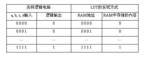
From this, it can be seen that LUT has the same functionality as a logic circuit. In fact, LUT has faster execution speed and greater scale.
Due to the high integration of LUT-based FPGAs, their device density ranges from tens of thousands to tens of millions of gates, capable of completing extremely complex sequential and combinational logic circuit functions, making them suitable for high-speed, high-density high-end digital logic circuit design fields. Their components mainly include programmable input/output units, basic programmable logic units, embedded SRAM, rich routing resources, embedded functional units, and embedded dedicated units. Major design and manufacturing companies include Xilinx, Altera, Lattice, Actel, Atmel, and QuickLogic, with Xilinx, Altera, and Lattice being the largest.
As mentioned earlier, FPGAs are set in their working state by RAM stored on the chip, so programming the internal RAM is required during operation. Users can adopt different programming methods based on different configuration modes. FPGAs have the following configuration modes:
Parallel mode: Parallel PROM, Flash configuration for FPGAs;
Master-slave mode: One PROM configures multiple FPGAs;
Serial mode: Serial PROM configures FPGAs;
Peripheral mode: Using the FPGA as a peripheral of a microprocessor, programmed by the microprocessor.
Currently, the two companies with the highest market share in FPGAs, Xilinx and Altera, produce SRAM-based FPGAs that require an external memory to save programs during use. Upon powering up, the FPGA reads data from the external memory into the internal RAM and enters the working state after configuration; when power is lost, the FPGA returns to a blank state, and the internal logic disappears. This way, FPGAs can be reused without needing a dedicated FPGA programmer; a general-purpose EPROM or PROM programmer suffices. Companies like Actel and QuickLogic offer antifuse technology FPGAs that can only be programmed once, featuring advantages such as radiation resistance, high and low-temperature tolerance, low power consumption, and fast speed, making them widely used in military and aerospace fields, but these FPGAs cannot be rewritten, making early development more complicated and costly. Lattice is the inventor of ISP technology, which has unique features in small-scale PLD applications. Early Xilinx products generally did not involve military and aerospace-grade markets, but now several products like Q Pro-R have entered this field.
1.2.2 FPGA Chip Structure
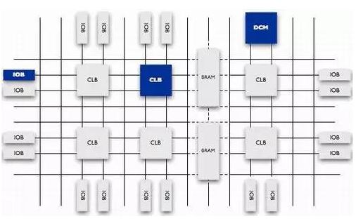
Currently, mainstream FPGAs are still based on LUT technology, far exceeding the basic performance of previous versions, and integrating commonly used functions (like RAM, clock management, and DSP) into hard (ASIC-type) modules. As shown in Figure 1-1 (Note: Figure 1-1 is just a schematic; each series of FPGAs has its corresponding internal structure), FPGA chips are mainly composed of six parts: programmable input/output units, basic programmable logic units, complete clock management, embedded block RAM, rich routing resources, embedded low-level functional units, and embedded dedicated hardware modules.
Figure 1-1 Internal structure of FPGA chip
The functions of each module are as follows:
1. Programmable Input/Output Units (IOB)
The programmable input/output unit, abbreviated as I/O unit, is the interface part between the chip and external circuits, fulfilling the driving and matching requirements for input/output signals under different electrical characteristics. Its schematic structure is shown in Figure 1-2. The I/O within the FPGA is classified into groups, with each group supporting different I/O standards independently. Through flexible configuration via software, it can adapt to different electrical standards and I/O physical characteristics, adjusting the size of driving currents and changing pull-up/pull-down resistors. Currently, the frequency of I/O ports is also increasing, with some high-end FPGAs supporting data rates of up to 2Gbps through DDR register technology.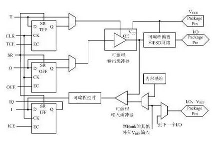 Figure 1-2 Schematic diagram of a typical IOB internal structure
External input signals can enter the internal FPGA through the storage unit of the IOB module or directly into the FPGA. When external input signals enter the FPGA through the storage unit of the IOB module, their hold time requirements can be relaxed, usually defaulting to 0.
To facilitate management and adapt to various electrical standards, the FPGA’s IOB is divided into several groups (banks), with the interface standard of each bank determined by its interface voltage VCCO. A bank can only have one VCCO, but different banks can have different VCCOs. Only ports with the same electrical standard can be connected together; having the same VCCO voltage is a basic condition for the interface standard.
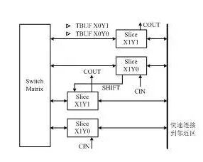
2. Configurable Logic Blocks (CLB)
CLB is the basic logic unit within the FPGA. The actual number and characteristics of CLBs vary depending on the device, but each CLB contains a configurable switch matrix, which consists of 4 or 6 inputs, some selection circuits (multiplexers, etc.), and flip-flops. The switch matrix is highly flexible and can be configured to handle combinational logic, shift registers, or RAM. In Xilinx’s FPGA devices, a CLB is composed of multiple (generally 4 or 2) identical slices and additional logic, as shown in Figure 1-3. Each CLB module can be used to implement combinational logic, sequential logic, and can also be configured as distributed RAM and distributed ROM.
Figure 1-3 Schematic diagram of a typical CLB structure
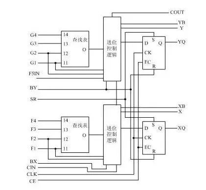
A slice is the basic logic unit defined by Xilinx, with its internal structure shown in Figure 1-4. A slice consists of two 4-input functions, carry logic, arithmetic logic, storage logic, and function multiplexers. The arithmetic logic includes an XOR gate (XORG) and a dedicated AND gate (MULTAND). An XOR gate allows a slice to perform 2-bit full addition operations, while the dedicated AND gate improves the efficiency of multipliers. Carry logic consists of dedicated carry signals and function multiplexers (MUXC) to achieve fast arithmetic addition and subtraction operations. The 4-input function generator is used to implement 4-input LUTs, distributed RAM, or 16-bit shift registers (the two input functions in the slice of the Virtex-5 series chips can be 6-input, allowing for 6-input LUTs or 64-bit shift registers); carry logic includes two fast carry chains to enhance the processing speed of the CLB module.
Figure 1-4 Schematic diagram of a typical 4-input Slice structure
3. Digital Clock Management Modules (DCM)
Most FPGAs in the industry provide digital clock management (all Xilinx FPGAs have this feature). Xilinx’s most advanced FPGAs offer digital clock management and phase-locked loops. Phase-locked loops can provide precise clock synthesis, reduce jitter, and implement filtering functions.
4. Embedded Block RAM (BRAM)
Most FPGAs have embedded block RAM, significantly expanding the application scope and flexibility of FPGAs. Block RAM can be configured as single-port RAM, dual-port RAM, content-addressable memory (CAM), and FIFO, among other common storage structures. RAM and FIFO are widely known concepts and will not be elaborated here. CAM memory has comparison logic in each of its internal storage units, and data written to CAM is compared with every piece of internal data, returning the addresses of all data that matches the port data, thus having wide applications in routing address switches. Besides block RAM, LUTs in FPGAs can also be flexibly configured into RAM, ROM, and FIFO structures. In practical applications, the number of internal block RAMs is also an important factor in chip selection.
The capacity of a single block RAM is 18k bits, with a bit width of 18 bits and a depth of 1024. It can be adjusted in bit width and depth as needed, but must meet two principles: first, the modified capacity (bit width x depth) cannot exceed 18k bits; second, the maximum bit width cannot exceed 36 bits. Of course, multiple block RAMs can be cascaded to form larger RAM, in which case it is only limited by the number of block RAMs within the chip, and the above two principles no longer apply.
5. Rich Routing Resources
Routing resources connect all units within the FPGA, and the length and process of the connections determine the driving capability and transmission speed of signals on the connections. FPGA chips have rich routing resources, categorized into four different types based on process, length, width, and distribution location. The first type is global routing resources, used for global clock and global reset/set routing within the chip; the second type is long line resources, used for high-speed signals and secondary global clock signal routing between chip banks; the third type is short line resources, used for logical interconnections and routing between basic logic units; the fourth type is distributed routing resources, used for proprietary clock, reset, and other control signal lines.
In practice, designers do not need to directly select routing resources; the layout router automatically selects routing resources to connect various module units based on the topology of the input logic netlist and constraint conditions. Essentially, the method of using routing resources is closely and directly related to the design results.
6. Low-Level Embedded Functional Units
Embedded functional modules mainly refer to DLL (Delay Locked Loop), PLL (Phase Locked Loop), DSP, and CPU soft cores. Increasingly rich embedded functional units make single-chip FPGAs become system-level design tools, enabling soft and hardware co-design capabilities, gradually transitioning to SOC platforms.
DLL and PLL have similar functions, capable of achieving high precision, low jitter clock multiplication and division, as well as duty cycle adjustment and phase shifting. Xilinx chips integrate DLLs, Altera chips integrate PLLs, and Lattice’s new chips integrate both PLL and DLL. PLL and DLL can be conveniently managed and configured through tools generated by IP cores. The structure of DLL is shown in Figure 1-5.
Figure 1-2 Schematic diagram of a typical IOB internal structure
External input signals can enter the internal FPGA through the storage unit of the IOB module or directly into the FPGA. When external input signals enter the FPGA through the storage unit of the IOB module, their hold time requirements can be relaxed, usually defaulting to 0.
To facilitate management and adapt to various electrical standards, the FPGA’s IOB is divided into several groups (banks), with the interface standard of each bank determined by its interface voltage VCCO. A bank can only have one VCCO, but different banks can have different VCCOs. Only ports with the same electrical standard can be connected together; having the same VCCO voltage is a basic condition for the interface standard.
2. Configurable Logic Blocks (CLB)
CLB is the basic logic unit within the FPGA. The actual number and characteristics of CLBs vary depending on the device, but each CLB contains a configurable switch matrix, which consists of 4 or 6 inputs, some selection circuits (multiplexers, etc.), and flip-flops. The switch matrix is highly flexible and can be configured to handle combinational logic, shift registers, or RAM. In Xilinx’s FPGA devices, a CLB is composed of multiple (generally 4 or 2) identical slices and additional logic, as shown in Figure 1-3. Each CLB module can be used to implement combinational logic, sequential logic, and can also be configured as distributed RAM and distributed ROM.
Figure 1-3 Schematic diagram of a typical CLB structure
A slice is the basic logic unit defined by Xilinx, with its internal structure shown in Figure 1-4. A slice consists of two 4-input functions, carry logic, arithmetic logic, storage logic, and function multiplexers. The arithmetic logic includes an XOR gate (XORG) and a dedicated AND gate (MULTAND). An XOR gate allows a slice to perform 2-bit full addition operations, while the dedicated AND gate improves the efficiency of multipliers. Carry logic consists of dedicated carry signals and function multiplexers (MUXC) to achieve fast arithmetic addition and subtraction operations. The 4-input function generator is used to implement 4-input LUTs, distributed RAM, or 16-bit shift registers (the two input functions in the slice of the Virtex-5 series chips can be 6-input, allowing for 6-input LUTs or 64-bit shift registers); carry logic includes two fast carry chains to enhance the processing speed of the CLB module.
Figure 1-4 Schematic diagram of a typical 4-input Slice structure
3. Digital Clock Management Modules (DCM)
Most FPGAs in the industry provide digital clock management (all Xilinx FPGAs have this feature). Xilinx’s most advanced FPGAs offer digital clock management and phase-locked loops. Phase-locked loops can provide precise clock synthesis, reduce jitter, and implement filtering functions.
4. Embedded Block RAM (BRAM)
Most FPGAs have embedded block RAM, significantly expanding the application scope and flexibility of FPGAs. Block RAM can be configured as single-port RAM, dual-port RAM, content-addressable memory (CAM), and FIFO, among other common storage structures. RAM and FIFO are widely known concepts and will not be elaborated here. CAM memory has comparison logic in each of its internal storage units, and data written to CAM is compared with every piece of internal data, returning the addresses of all data that matches the port data, thus having wide applications in routing address switches. Besides block RAM, LUTs in FPGAs can also be flexibly configured into RAM, ROM, and FIFO structures. In practical applications, the number of internal block RAMs is also an important factor in chip selection.
The capacity of a single block RAM is 18k bits, with a bit width of 18 bits and a depth of 1024. It can be adjusted in bit width and depth as needed, but must meet two principles: first, the modified capacity (bit width x depth) cannot exceed 18k bits; second, the maximum bit width cannot exceed 36 bits. Of course, multiple block RAMs can be cascaded to form larger RAM, in which case it is only limited by the number of block RAMs within the chip, and the above two principles no longer apply.
5. Rich Routing Resources
Routing resources connect all units within the FPGA, and the length and process of the connections determine the driving capability and transmission speed of signals on the connections. FPGA chips have rich routing resources, categorized into four different types based on process, length, width, and distribution location. The first type is global routing resources, used for global clock and global reset/set routing within the chip; the second type is long line resources, used for high-speed signals and secondary global clock signal routing between chip banks; the third type is short line resources, used for logical interconnections and routing between basic logic units; the fourth type is distributed routing resources, used for proprietary clock, reset, and other control signal lines.
In practice, designers do not need to directly select routing resources; the layout router automatically selects routing resources to connect various module units based on the topology of the input logic netlist and constraint conditions. Essentially, the method of using routing resources is closely and directly related to the design results.
6. Low-Level Embedded Functional Units
Embedded functional modules mainly refer to DLL (Delay Locked Loop), PLL (Phase Locked Loop), DSP, and CPU soft cores. Increasingly rich embedded functional units make single-chip FPGAs become system-level design tools, enabling soft and hardware co-design capabilities, gradually transitioning to SOC platforms.
DLL and PLL have similar functions, capable of achieving high precision, low jitter clock multiplication and division, as well as duty cycle adjustment and phase shifting. Xilinx chips integrate DLLs, Altera chips integrate PLLs, and Lattice’s new chips integrate both PLL and DLL. PLL and DLL can be conveniently managed and configured through tools generated by IP cores. The structure of DLL is shown in Figure 1-5.
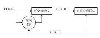
Figure 1-5 Schematic diagram of a typical DLL module
7. Embedded Dedicated Hard Cores
Embedded dedicated hard cores refer to powerful hard cores (Hard Cores) within FPGAs, equivalent to ASIC circuits. To enhance FPGA performance, chip manufacturers integrate dedicated hard cores within the chip. For example, to improve multiplication speed, mainstream FPGAs include dedicated multipliers; to accommodate communication bus and interface standards, many high-end FPGAs integrate serial/parallel transceivers (SERDES), achieving transceiver speeds of dozens of Gbps.
Xilinx’s high-end products not only integrate Power PC series CPUs but also embed DSP Core modules, with corresponding system-level design tools being EDK and Platform Studio, thus proposing the concept of System on Chip (SoC). Through platforms like PowerPC, Microblaze, and Picoblaze, standard DSP processors and their related applications can be developed, achieving SoC development objectives.
1.2.3 Concepts of Soft Cores, Hard Cores, and Firm Cores
IP (Intelligent Property) cores refer to integrated circuit cores with intellectual property rights, which are verified macro-modules with specific functions, independent of chip manufacturing processes, and can be ported to different semiconductor processes. In the SOC stage, IP core design has become an important task for ASIC design companies and FPGA providers, reflecting their strength. For FPGA development software, the richer the IP cores provided, the more convenient the user’s design, and the higher its market share. Currently, IP cores have become the basic unit of system design and are exchanged, transferred, and sold as independent design results.
Based on the provision method of IP cores, they are usually divided into three categories: soft cores, hard cores, and firm cores. In terms of the cost of completing IP cores, hard cores are the most expensive; in terms of usage flexibility, soft cores have the highest reusability.
Soft cores in the EDA design field refer to register transfer level (RTL) models before synthesis; specifically, in FPGA design, it refers to hardware language descriptions of circuits, including logic descriptions, netlists, and documentation. Soft cores undergo only functional simulation and require synthesis and layout routing to be usable. Their advantages include high flexibility and strong portability, allowing user configuration; their disadvantages include lower predictability of modules, with potential errors in subsequent designs, carrying certain design risks. Soft cores are the most widely used form of IP cores.
Firm cores in the EDA design field refer to netlists with planar layout information; specifically, in FPGA design, they can be seen as soft cores with layout planning, typically provided in a mixed form of RTL code and corresponding specific process netlists. By combining RTL descriptions with specific standard cell libraries for synthesis optimization design, a gate-level netlist is formed, which can then be used through layout routing tools. Compared to soft cores, firm cores have slightly lower design flexibility but significantly improved reliability. Currently, firm cores are also one of the mainstream forms of IP cores.
Hard cores in the EDA design field refer to verified design layouts; specifically, in FPGA design, they refer to designs that are fixed in layout and process, having undergone front-end and back-end verification, which designers cannot modify. The reasons for the inability to modify are twofold: first, system design has very strict timing requirements for each module, not allowing disruption of existing physical layouts; second, the requirement to protect intellectual property does not permit designers to make any changes. The characteristic of non-modifiability of IP hard cores makes their reuse somewhat difficult, so they can only be used for certain specific applications, with a narrower usage range.
Source | Hardware Ten Thousand Whys
☞ Business Cooperation: ☏ Please call 010-82306118 / ✐ Or send an email to [email protected]
Click here for “Read the original text”, directly reaching Electronic Technology Application Official Website