Click the blue text to follow us
Semiconductors
In the process of semiconductor process research and manufacturing, precise characterization techniques are the core link to ensure device performance and yield.
This article systematically elaborates on the technical principles and typical application scenarios of six key analytical instruments used in semiconductor process characterization.
1. Secondary Ion Mass Spectrometry (SIMS)
Technical Principle:
SIMS bombards the sample surface with a high-energy ion beam (such as Cs⁺, O₂⁻, Ar⁺), exciting atoms, molecules, and secondary ions.

The energy analyzer and mass analyzer work together to filter secondary ions by energy and mass, ultimately generating a mass spectrum through an ion detector. This technology can achieve vertical depth profiling of elemental composition (with depth resolution reaching the nanometer level) and lateral two-dimensional imaging, with detection limits reaching ppm (parts per million) to ppb (parts per billion) levels.
Application Scenarios:
Doping concentration analysis: Monitoring the concentration distribution of dopants such as boron and phosphorus during ion implantation processes.
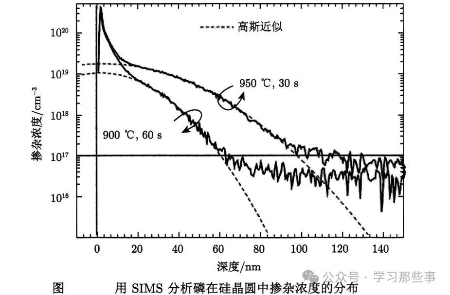
For example, the Gaussian distribution curve of phosphorus doping concentration after oxidation annealing shown in the figure above can evaluate the impact of the annealing process on dopant diffusion.
Interface contamination detection: Analyzing the content of metal impurities (such as Fe, Cu) at the oxide/silicon interface to assess the effectiveness of cleaning processes.
Molecular structure characterization: Identifying residues of organic photoresists or components of polymer passivation layers.
Variant Technology:
Time-of-Flight SIMS (TOF-SIMS) identifies elements by measuring the time-of-flight differences of secondary ions over a fixed distance.

It is suitable for non-destructive analysis of extremely thin surface layers (<1nm), such as detecting hydrogen content in gate dielectric layers.
2. Atomic Force Microscopy (AFM)
Technical Principle:
AFM utilizes the changes in forces (van der Waals forces, electrostatic forces, etc.) between the probe and the sample surface atoms to drive the deflection of a cantilever.
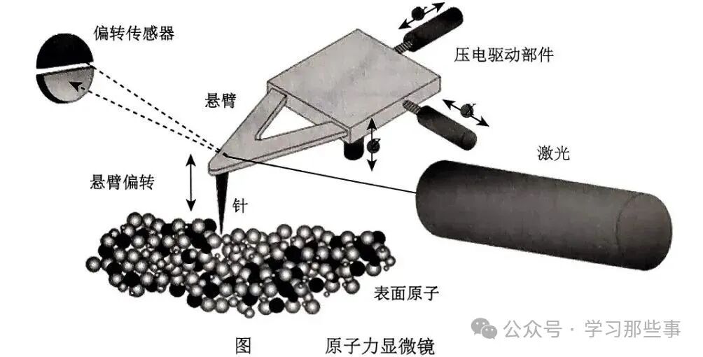
Laser interferometry accurately measures the deformation of the cantilever, reconstructing the surface morphology of the sample, with a vertical resolution of up to 0.1nm.
Application Scenarios:
Surface roughness measurement: Evaluating the global flatness of wafer surfaces after chemical mechanical polishing (CMP) to optimize polishing fluid formulations and process parameters.
Nano-structure characterization: Observing the sidewall morphology of photoresist patterns and detecting line edge roughness (LER), providing feedback for extreme ultraviolet lithography (EUV) processes.
Mechanical property testing: Analyzing the Young’s modulus of low-k materials through force-distance curves to assess mechanical stability.
Limitations: Scanning speed is relatively slow (usually <1Hz/pixel), making it difficult to meet the demand for large-area rapid inspection.
3. Auger Electron Spectroscopy (AES)
Technical Principle:
AES utilizes a high-energy electron beam to excite inner-shell electron transitions in surface atoms of the sample, achieving qualitative analysis of elements by detecting Auger electron energy.

Its information depth is limited to 1-5nm at the surface, with high sensitivity to light elements (such as B, C, N).
Application Scenarios:
Thin film composition analysis: Determining the oxygen content at the interface of metal gates (such as TiN, TaN) and high-k dielectrics to optimize atomic layer deposition (ALD) processes.
Oxide layer thickness measurement: Combining the exponential decay law of Auger electron yield with depth to calibrate the thickness of gate oxide layers (<5nm).
Failure analysis: Locating surface composition changes in metal interconnects that have failed due to electromigration, such as the segregation of Cu in Al-Cu alloys.
Technical Features: Spatial resolution better than 10nm, but requires ultra-high vacuum conditions (<10⁻⁹ Torr).
4. X-ray Photoelectron Spectroscopy (XPS)
Technical Principle:
XPS uses monochromatic X-rays (such as Al Kα=1486.6eV) to irradiate the sample, exciting photoelectrons to escape.
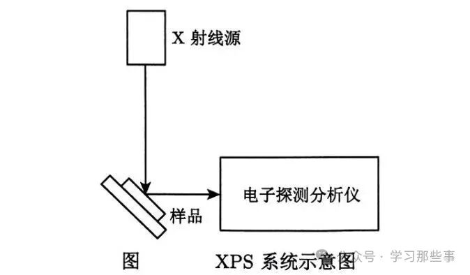
By measuring the kinetic energy of photoelectrons
Ek=hν-Eb-φ
the chemical state of elements is determined, where Eb is the electron binding energy and φ is the instrument work function.
Application Scenarios:
Chemical state analysis: Identifying the bonding states of Si-Si and Si-Me (metal) during the formation of silicides to optimize silicide process temperatures.
Interface reaction studies: Analyzing the composition of the interfacial layer (IL) between high-k dielectrics (such as HfO₂) and silicon substrates to assess interface state density.
Contamination control: Detecting the residual amount of hydrocarbons on wafer surfaces after cleaning (C1s peak intensity).
Technical Advantages: Non-destructive testing, but information depth is limited to 2-3nm at the surface, requiring argon ion sputtering for depth profiling.
5. Transmission Electron Microscopy (TEM)
Technical Principle:
TEM transmits a high-voltage accelerated electron beam (typically 100-300kV) through ultra-thin samples (<100nm), focusing the image using electromagnetic lenses.

The energy loss spectrometer (EELS) can simultaneously analyze the characteristics of electron energy loss, obtaining information on elemental distribution and chemical bonding.
Application Scenarios:
Defect characterization: Observing dislocation loops and stacking faults in shallow junctions of silicon to evaluate ion implantation damage repair processes.
Three-dimensional structure reconstruction: Analyzing the three-dimensional morphology of FinFET devices in conjunction with focused ion beam (FIB) slicing technology.
Metallization analysis: Studying the lattice matching of cobalt silicide (CoSi₂) at the silicon contact interface to optimize ohmic contact performance.
Sample preparation challenges: Requires mechanical grinding, chemical polishing, and ion thinning to obtain electron-transparent areas, with preparation cycles lasting several hours.

The above analytical techniques cover a complete dimension from nano-level morphology characterization (AFM), surface chemical analysis (XPS/AES) to sub-atomic level structure resolution (TEM), forming a complementary relationship in semiconductor process development.
For example, in advanced process nodes (<7nm), it is necessary to use SIMS to monitor dopant diffusion, AES to analyze interface oxide layers, and TEM to observe strained silicon channel structures to systematically optimize process parameters.
To learn more and enjoy more benefits, you can join our knowledge community, where you can ask questions, and we will do our best to help you!


To facilitate communication among peers, this public account has created a series of technical discussion groups, and all colleagues are welcome to join! You can add the group owner on WeChat (WeChat ID: xxnxs5262692) to apply for group membership!
① Chip packaging and testing process discussion group
② Failure analysis and reliability discussion group
③ Quality system control discussion group
④ Advanced packaging process discussion group
⑤ Wafer manufacturing process discussion group
⑥ Analog circuit design discussion group
⑦ Wire bonding process discussion group
⑧ Packaging equipment technology discussion group
⑨ Electronic assembly technology discussion group
⑩ Thinning and dicing technology discussion group
You can reply to “join group” in the background or scan the group owner’s WeChat below to apply for group membership.

That’s all for sharing. If you have any needs, please leave a message in the background!

Learning About Those Matters
Images are sourced from the internet. If there is any infringement, please inform us for deletion.