During the use of I2C, we may observe half-high levels or glitch phenomena. This article attempts to explain the causes of these phenomena and their impact on applications. The main content is as follows:
1. Glitch/Half-High Level Phenomenon
2. Characteristics of Glitches/Half-High Levels
3. Causes of Glitches
4. Is the Existence of Glitches Reasonable?
5. Causes of Half-High Levels
6. How to Evaluate the Impact of Glitches/Half-High Levels on Applications
7. Selection of Level Shift (Level Shifting Chips)
8. What Are We Setting When We Set the Frequency?
9. Summary
1. Glitch/Half-High Level Phenomenon
Common glitches are as follows:
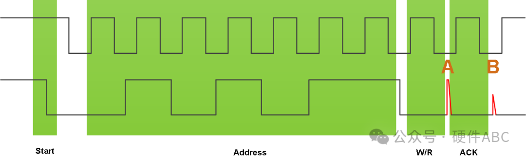
(Here, taking I2C addressing as an example, glitches often occur at points A and B, with varying widths)
Common half-high levels are as follows:
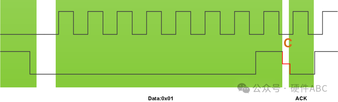
(Here, taking writing to a register after addressing as an example, half-high levels often occur at point C)
2. Characteristics of Glitches/Half-High Levels
From the above examples, it can be seen that the occurrence of glitches/half-high levels is concentrated near ACK. Why is that? In other words, do glitches/half-high levels occur elsewhere? This requires us to analyze the characteristics of ACK.
Characteristics of the ACK bit: Represents the transition of the SDA controller.
Combining the examples,
Point A, SDA controller: Master ➡️ Slave
Point B, SDA controller: Slave ➡️ Master
Point C, SDA controller: Master ➡️ Slave
So, why does the transition of the SDA controller lead to this “abnormal” waveform?
3. Causes of Glitches
The logic before and after points A/B: After the Master sends the W/R bit, it releases SDA → SDA is pulled high by the bus → Slave pulls SDA low to ACK → After the Slave acknowledges, it releases SDA → SDA is pulled high by the bus → Master pulls SDA low, taking control of SDA. Thus, the cause of the glitch seems to be clear:
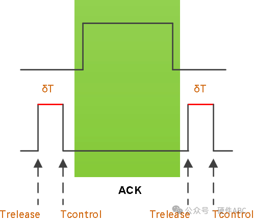
Here, we define: Trelease as the moment SDA is released, Tcontrol as the moment SDA is controlled, then δT=Tcontrol-Trelease represents the width of the glitch.
If δT>0, glitches occur at points A and B;
If δT≤0, there are no glitches;
4. Is the Existence of Glitches Reasonable?
Reasonable.
The I2C protocol specifies the maximum value of tVD:ACK, which refers to the time after SCL falls when the master releases SDA, as well as the time the slave controls SDA. In other words, the specification does not specify the order of these two events, so for communication between different manufacturers’ Masters and Slaves, δT can have various possibilities as described in (3. Causes of Glitches).
5. Causes of Half-High Levels
In a normally functioning I2C system, there are only two levels: VCC and GND. If a stable half-high level like point C is observed in the measured waveform, there is only one possibility: SDA is pulled high while also being pulled low, and the pull-up/pull-down capabilities are roughly equal.
Generally speaking, for I2C applications, pull-up resistors are usually in the kΩ range, which is less than the pull-down capability. Therefore, the occurrence of half-high levels can have two possibilities:
a. The MCU simulates I2C through GPIO, and the GPIO output mode is set to Push-Pull.
b. A buffer is added between the Master and Slave for level shifting, such as the 74LVC1T45, which has a direction control DIR function for Push-Pull output. If the direction control is not timely, the waveform at point C will occur. The Slave has already taken control of SDA and pulled it low to ACK, but the buffer is still outputting a Push-Pull pull-up, causing both to pull up/down simultaneously, resulting in a half-high level on SDA, with power consumption typically reaching around 10mA.
6. How to Evaluate the Impact of Glitches/Half-High Levels on Applications
Recall one of the strictest rules of I2C: During the high level of SCL, SDA must remain stable.
Therefore, as long as the occurrence of SDA glitches/half-high levels does not happen during the high level of SCL, it will not affect communication, as mentioned at points A, B, and C.
7. Selection of Level Shift (Level Shifting Chips)
Level Shifters are mainly divided into two types: passFET-based Switch type and logic-controlled Buffer type. The passFET-based Switch type is inherently friendly to I2C, so it is recommended to choose the switch type for I2C Level Shifters. (The architecture/differences of Level Shifters are not the focus of this article, so we will stop here.)
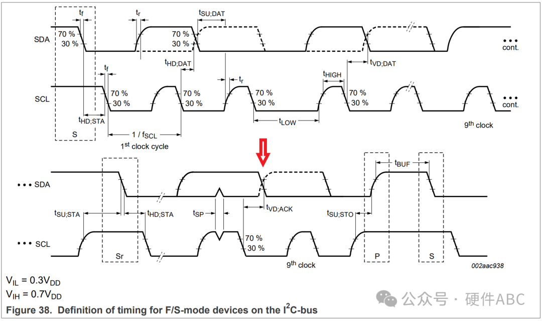
Let’s look at what conditions need to be met when selecting a Level Shifter to avoid impacting applications, assuming a case of level conversion.
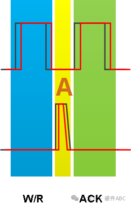
The black waveform is from the Master side, and the red waveform is from the Slave side. Based on the previous analysis, as long as the yellow and green areas do not overlap, it will not affect the application. For safety, the wider this area is, the greater the margin.
8. What Are We Setting When We Set the Frequency?
When using a host computer to read and write chip registers, there is often an option to set the I2C frequency: 100kHz, 400kHz, or 1MHz, etc.
The higher the frequency, the shorter the SCL period, and the shorter the time interval between two SCLs. The Slave can respond to SCL and change SDA in a shorter time.
For example: For a 1MHz Master, a Slave that only supports 400kHz may not be able to respond with an ACK within half a cycle. Furthermore, even if this Slave supports extending the low level of SCL, it may still fail to respond correctly to SCL and send Data.
When using an MCU to simulate I2C with GPIO, the shorter the delay between pulling GPIO high/low between adjacent instructions, the higher the communication frequency of the MCU. When communication anomalies occur, it is often found that increasing the delay can restore normal communication.
Therefore, for the same Master, the higher the frequency supported by the Slave, the lower the likelihood of glitches occurring.
9. Summary
Communication failures can be analyzed through waveforms;
Successful communication can also be analyzed through margins.
Take it easy!
This article is entirely the author’s ramblings, and comments are welcome in the comment section.