Follow 【RF Academy】 to learn something new every day! Join groups/recruitment/repost/collaborate/contribute/promote, add WeChat: RF_Centered Everything in nature has its unique characteristics, and what we can do is only to explore these properties and utilize them for our benefit. In the field of electronics, materials can typically be classified based on their electrical conductivity characteristics into: conductors, insulators, and semiconductors, which lie between conductors and insulators. Today, we are going to talk about this special material – semiconductors. Semiconductors are the backbone of modern electronic technology, with diodes, transistors, and ICs all made from semiconductor materials. In the foreseeable future, they will be key components in most electronic systems, serving communication, signal processing, computing, and control applications in both consumer and industrial markets.Introduction to Semiconductor Materials The following diagram is a schematic from the public network showing the electrical conductivity characteristics of materials. The conductivity of a material can be represented by resistivity ρ, or conductivity σ, and these two Greek letters are particularly apt; conductivity σ is the reciprocal of resistivity ρ. Insulators have relatively low conductivity, such as glass or quartz, while conductors have relatively high conductivity, such as silver, copper, aluminum, and gold. Here, I would like to remind everyone that although gold is expensive, its conductivity is not very good; the best is silver, the purer the better, followed by copper, the purer the better, while brass is just average. Additionally, some conductors can become even more conductive under certain conditions, known as superconductors. The conductivity of semiconductors lies between that of insulators and conductors, and they are usually sensitive to temperature, light, magnetic fields, and trace impurity atoms. For example, adding about 10 boron atoms (known as dopants) per million silicon atoms can increase its conductivity by a thousand times. Common semiconductor materials include silicon (Si), germanium (Ge), and now widely used gallium nitride and gallium arsenide.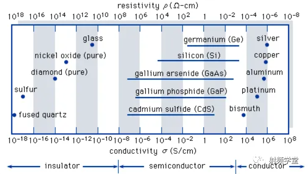 The study of semiconductor materials began in the 19th century, during which an important Russian chemist, Dmitri Ivanovich Mendeleev, summarized and organized the periodic table of elements.
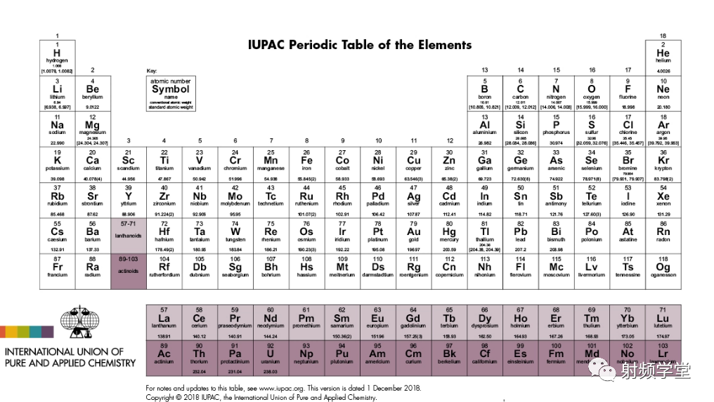 We also owe thanks to the contributions of the old Zhu family regarding the periodic table of elements in China.
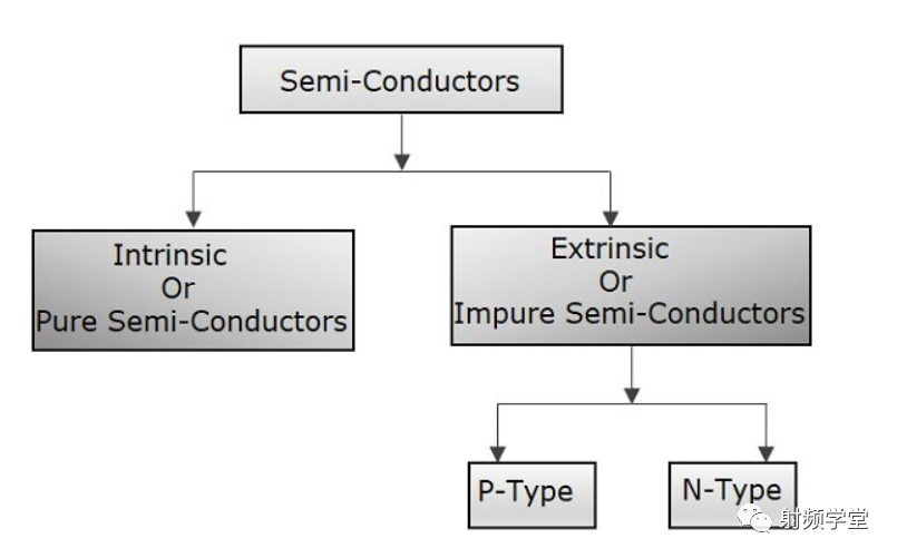
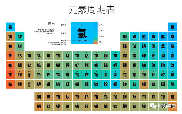 Elemental semiconductors are composed of a single type of atom, such as silicon (Si), germanium (Ge), and tin (Sn) listed in group IV of the periodic table, while selenium (Se) and tellurium (Te) are listed in group VI of the periodic table. However, there are many compound semiconductors composed of two or more elements. For example, gallium arsenide (GaAs) is a binary III-V compound formed from gallium (Ga) from group III and arsenic (As) from group V. Ternary compounds can be formed from elements from three different groups—for example, mercury indium telluride (HgIn2Te4), a II-III-VI compound. They can also be formed from elements from two groups, such as aluminum gallium arsenide (AlxGa1-xAs), a ternary III-V compound where both Al and Ga come from group III, and the subscript x relates to the composition of the two elements from 100% Al (x = 1) to 100% Ga (x = 0). Pure silicon is the most important material for integrated circuit applications, while III-V binary and ternary compounds are crucial for optoelectronics. Before the invention of the bipolar transistor in 1947, semiconductors were only used as two-terminal devices, such as rectifiers and photodiodes. In the early 1950s, germanium was the primary semiconductor material. However, it proved unsuitable for many applications because devices made from this material exhibited high leakage currents even at moderately elevated temperatures. Since the early 1960s, silicon has become the most widely used semiconductor, almost replacing germanium as the material for device manufacturing. The main reasons for this are twofold: (1) silicon devices exhibit much lower leakage currents, and (2) silicon dioxide (SiO2), a high-quality insulator, can easily be used as part of silicon-based devices. Therefore, silicon technology has become very advanced and widespread, with silicon devices accounting for over 95% of global sales of all semiconductor products. Many compound semiconductors possess certain specific electrical and optical properties that are superior to their silicon counterparts. These semiconductors, especially gallium arsenide, are primarily used in optoelectronic and certain radio frequency (RF) applications.Electrical Properties of Semiconductor Materials Semiconductor materials can also be classified into two categories: pure semiconductor materials and doped semiconductor materials. The extremely pure form of semiconductors is called intrinsic semiconductors. However, this pure form has very low conductivity. To enhance the conductivity of intrinsic semiconductors, it is best to add some impurities. This process of adding impurities is called doping. Now, this doped intrinsic semiconductor is referred to as extrinsic semiconductors.
 Pure semiconductor materials are primarily silicon and germanium, which are single-crystal materials. The atoms are arranged in a three-dimensional periodic manner. Part A of the figure shows a simplified two-dimensional representation of intrinsic (pure) silicon crystals containing negligible impurities. Each silicon atom in the crystal is surrounded by four nearest neighbors. Each atom has four electrons in its outer shell and shares these electrons with its four neighbors. Each shared electron pair forms a covalent bond. The attraction between the electrons and the two atomic nuclei binds the two atoms together. For isolated atoms (for example, in gas rather than in crystal), the electrons can only have discrete energy levels. However, when a large number of atoms gather together to form a crystal, the interactions between atoms cause discrete energy levels to spread into energy bands. When there is no thermal vibration (i.e., at low temperatures), the electrons in an insulator or semiconductor crystal will completely fill many energy bands, while the remaining energy bands will be empty. The highest filled band is called the valence band. The next energy band is the conduction band, which has an energy gap (the gap in a crystal insulator is much larger than that in a semiconductor) between it and the valence band. This energy gap, also known as the bandgap, is a region in the crystal where electrons cannot have energy. The bandgap of most important semiconductors ranges from 0.25 to 2.5 electron volts (eV). For example, silicon has a bandgap of 1.12 eV, while gallium arsenide has a bandgap of 1.42 eV. In contrast, the bandgap of well-crystallized insulator diamond is 5.5 eV.
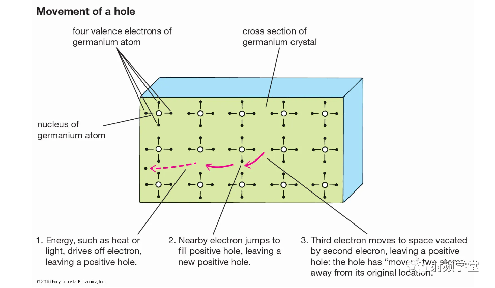
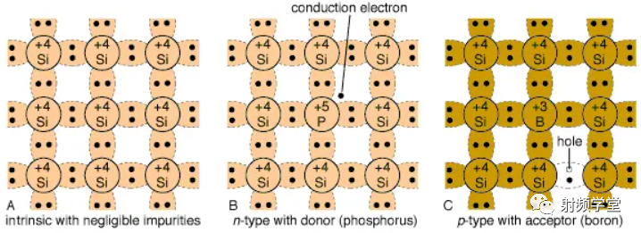 At low temperatures, electrons in semiconductors are bound within their respective energy bands in the crystal. Therefore, they cannot conduct electricity. At higher temperatures, thermal vibrations may break some covalent bonds, resulting in free electrons that can participate in current conduction. Once electrons leave the covalent bonds, electron vacancies associated with those bonds appear. These vacancies can be filled by adjacent electrons, causing the vacancy position to move from one crystal location to another. This vacancy can be viewed as a fictitious particle known as a “ hole,” which carries a positive charge and moves in the opposite direction to the electrons. When an electric field is applied to the semiconductor, both free electrons (now in the conduction band) and holes (left in the valence band) move through the crystal, generating current. The electrical conductivity of the material depends on the number of free electrons and holes (charge carriers) per unit volume and the rate at which these carriers move under the influence of the electric field. In intrinsic semiconductors, there are equal numbers of free electrons and holes. However, electrons and holes have different mobilities. That is to say, they move at different speeds in the electric field. For example, for intrinsic silicon at room temperature, the electron mobility is 1,500 square centimeters/volt-second (cm2/V·s)—that is, under an electric field of 1 volt per centimeter, electrons will move at a speed of 1,500 centimeters per second—while the hole mobility is 500 cm2/V·s. The mobility of electrons and holes in specific semiconductors typically decreases with increasing temperature.
 The conductivity of intrinsic semiconductors is very poor at room temperature. To achieve higher conductivity, impurities can be intentionally introduced (usually at a concentration of parts per million of the host atoms). This is called doping, a process to increase conductivity, although there is some mobility loss. For example, if a silicon atom is replaced by an atom with five outer electrons, such as arsenic (see part B of the figure), four of those electrons form covalent bonds with four neighboring silicon atoms. The fifth electron becomes a conduction electron, donating to the conduction band. Silicon becomes an n-type semiconductor because electrons are added. The arsenic atom is the donor. Similarly, part C of the figure shows that if a silicon atom is replaced by an atom with three outer electrons (such as boron), it accepts an extra electron, forming four covalent bonds around the boron atom, creating a positively charged hole in the valence band. This results in a p-type semiconductor, where boron acts as the acceptor.
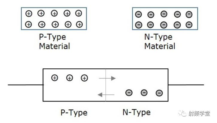 In the p-side, holes are the majority carriers, hence referred to as majority carriers. There will also be a small number of thermally generated electrons; these are called minority carriers. On the n-side, electrons are the majority carriers, while holes are the minority carriers. Near the junction, there is a region devoid of free charge carriers. This region is called the depletion layer, which behaves as an insulator.
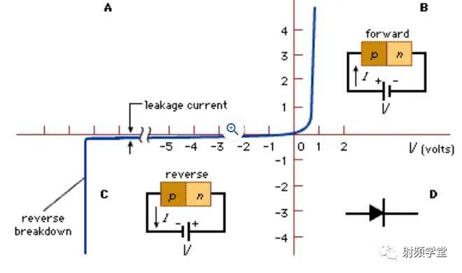 The most important characteristic of p-n junctions is that they can rectify. Part A of the figure shows the current-voltage characteristics of a typical silicon p-n junction. When a forward bias is applied to the p-n junction (i.e., a positive voltage is applied to the p-side relative to the n-side, as shown in part B of the figure), the majority charge carriers move across the junction, allowing a large current to flow. However, when a reverse bias is applied (as shown in part C of the figure), the charge carriers introduced by impurities move away from the junction in the opposite direction, resulting in only a small leakage current. As the reverse bias increases, the leakage current remains very small until the critical voltage is reached, at which point the current suddenly increases. This sudden increase in current is known as junction breakdown, which, if the power dissipation generated is limited to safe values, is typically a non-destructive phenomenon. The applied forward voltage is usually less than 1 volt, but the reverse critical voltage, known as breakdown voltage, can range from less than 1 volt to several thousand volts, depending on the impurity concentration parameters of the junction and other devices. The applications of p-n junctions form the foundation of modern semiconductors, although many more junctions have been invented, such as PNP or NPN, the application of p-n junctions in modern electronics remains unshakable.References
- https://www.techtarget.com/whatis/definition/semiconductor
- https://www.autodesk.com/products/fusion-360/blog/transistors-101-detailed-introduction/
- https://byjus.com/jee/transistor/
- https://byjus.com/jee/semiconductors/
- https://www.thoughtco.com/what-is-a-transistor-2698913
- https://www.britannica.com/science/semiconductor
Note: 【RF Academy】 reposts, all original articles belong to the original authors. Sharing aims to learn; if there are any objections, please contact RF Academy to delete or change. Wishing you much learning and gain at RF Academy!Essential for RF Learning
【RF Material Download】【Essential RF Basics】【Must-Read Excellent Articles