Click the blue words to follow us
1. Microcontroller Parallel External Expansion System
1. Microcontroller Parallel External Expansion System
External expansion is an important aspect of building a microcontroller system, which can be categorized into two types:
Memory expansion and I/O expansion;
There are two methods for external expansion: parallel expansion and serial expansion.
2. Microcontroller Parallel Expansion Bus
Memory expansion includes program memory and data memory, while all other expansion content is collectively referred to as I/O expansion.
From the structure diagram of the expansion system, it can be seen that expansion is conducted via the system bus. The so-called bus is a set of common signal lines that connect various expansion components of the microcontroller, serving as a shared path for the system, connecting all expansion components to transmit data, address, and control signals.
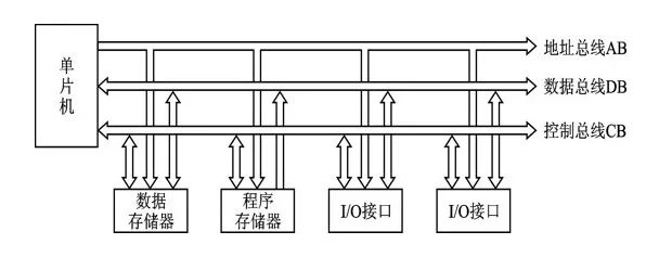
Microcontroller Parallel Expansion System Structure Diagram
3. Composition of the Parallel Expansion Bus
The parallel expansion bus consists of three components: the address bus, data bus, and control bus.
The address bus (Address Bus, abbreviated AB) transmits address signals used for addressing external memory units and I/O ports. The address bus is unidirectional.
The data bus (Data Bus, abbreviated DB) is used to transmit data, status, instructions, and commands. The bit width of the data bus should match the word length of the microcontroller. The data bus is bidirectional.
The control bus (Control Bus, abbreviated CB) is a set of control signal lines. The transmission of a control signal is unidirectional, but the control bus composed of signal lines from different directions should be represented as bidirectional.
The bus structure can improve the reliability of the system and increase its flexibility.
4. 80C51 Microcontroller Parallel Expansion Bus
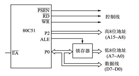
80C51 Microcontroller Parallel Expansion Bus Structure Diagram
(1) The 8-bit port line of P0 acts as the low address/data line
The low address/data line refers to the low 8 bits of address A7~A0, while the data line corresponds to D7~D0.
After separating the address and data, an additional 8-bit latch is required to store the separated address, using ALE as the latch control signal.
(2) The port line of P2 serves as the high address line
P2 is used only as a high address line, and combined with the low 8-bit address provided by P0, a complete 16-bit address bus is formed, allowing the microcontroller’s external addressing range to reach 64K units.
(3) Control Signals
In addition to address and data lines, the system expansion also requires the microcontroller to provide some control signal lines, which constitute the control bus of the expansion system. These control signals include:
-
Using ALE as the address latch selection signal to achieve low 8-bit address latching.
-
Using /PSEN signal as the read selection signal for the expansion program memory.
-
Using /EA signal as the selection signal for internal and external program memory.
-
Using /RD and /WR as the read/write selection signals for the expansion data memory and I/O ports.
5. I/O Addressing and Chip Selection of the Parallel Expansion System
The connection of data lines and control signal lines is relatively simple, while the connection of address lines is more complex, involving I/O addressing and chip selection issues.
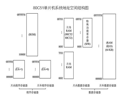
The external expansion address space of the microcontroller is related to its memory system. The memory system of the 80C51 microcontroller and the structure of the external expansion address space are shown in the diagram below.
6. Chip Selection Technology
To expand the microcontroller system, the first issue to address is the addressing problem, i.e., how to find the expansion chip to access and the target unit within the chip.
To perform chip selection, expansion chips typically have one or more chip selection signal pins (commonly referred to as CE or CS). Thus, the addressing problem boils down to how to generate valid chip selection signals. Common chip selection methods (i.e., addressing methods) include wired selection and decoding methods.
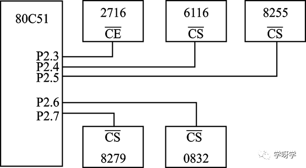
(1) Wired Selection Addressing
Wired selection means directly using bit address signals as chip selection signals. When in use, simply connect the address lines directly to the chip’s chip selection signal pins.
The main characteristic of wired selection addressing is its simplicity, making it suitable for smaller microcontroller systems. Assuming the microcontroller system has expanded program memory chip 2716, data memory chip 6116, parallel interface chip 8255, keyboard/display interface chip 8279, and D/A converter chip 0832, the expanded chip selection connections using wired selection are shown in the diagram below.
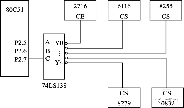
(2) Decoding Method Addressing
The decoding method uses a decoder to decode high address bits, with its decoded output serving as the chip selection signal for the expansion chip. This is a commonly used addressing method that effectively utilizes storage space and is suitable for large capacity, multi-chip system expansions. The system expansion chip selection connections using decoding method are illustrated in the diagram below.
2. Classification of Memory
(1) Mask Read-Only Memory
Mask Read-Only Memory is programmed by the semiconductor manufacturer, meaning programming is completed during the manufacturing process. Since the programming process uses a mask process, it is referred to as Mask ROM.
(2) Programmable Read-Only Memory (PROM)
PROM (Programmable Read-Only Memory) chips have no program information when they leave the factory; the program is written by the user at the development site. However, this type of ROM chip can only be written once, and its content cannot be modified once written.
(3) Erasable Programmable Read-Only Memory (EPROM)
EPROM (Erasable Programmable Read-Only Memory) chips are written by the user but allow for repeated erasure and rewriting. EPROM is erased using ultraviolet light.
(4) Electrically Erasable Programmable Read-Only Memory (E2PROM)
E2PROM (Electrically Erasable Programmable Read-Only Memory) is a type of ROM chip that is programmed and erased using electrical signals. It allows for reading and writing of individual storage units through read/write operations, similar to RAM, but with slower writing speeds, yet it retains information after power loss.
(5) Flash Memory (Flash ROM)
Flash memory, fully known as Flash Programmable/Erasable Read-Only Memory, is also referred to as Flash memory or FPEROM (Flash Programmable and Erasable Read-Only Memory).
In the microcontroller system, data memory is used to store data that can be modified at any time. Data memory expansion uses random access memory chips, abbreviated as RAM.
RAM allows both read and write operations, but it is volatile memory, meaning information is lost when power is turned off.
RAM is further divided into static (SRAM) and dynamic (DRAM) based on working method.
3. Parallel Expansion of Memory
The expanded program memory is referred to as external ROM, while the expanded data memory is referred to as external RAM.
(1) Parallel Expansion of Program Memory
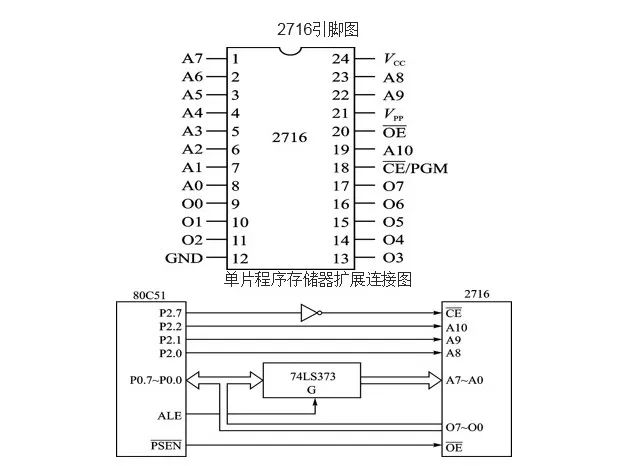
Program memory expansion uses read-only memory chips, illustrated with the simplest 2716 chip as an example. The main pin functions of the 2716 pinout are as follows:
A10~A0: 11-bit address.
O7~O0: Data output.
CE/PGM: Dual-function control line.
OE: Output enable signal.
VPP: Programming power supply. When programming the chip, +25 V programming voltage is applied; during use, +5 V power supply is applied.
(2) Main Content of Memory Expansion
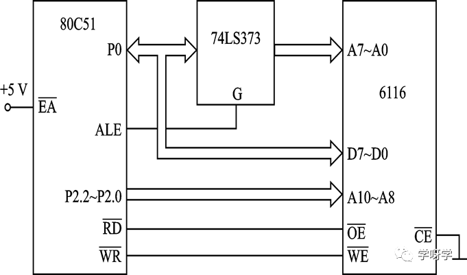
The main content of memory expansion involves the connection of address lines, data lines, and control lines. The storage capacity of the 2716 is 2 KB, requiring 11 bits of address (A10~A0) for memory unit addressing. To achieve this, first connect the A7~A0 pins of the chip to the 8-bit address output of the address latch, and then connect the A10~A8 pins to P2 port lines P2.2~P2.0. Using wired selection for chip selection, only one of the remaining high address lines (P2.7) needs to be connected to the CE pin of the 2716.
The connection of data lines is relatively simple; just connect the data output pins of the memory chip to the P0 port lines of the microcontroller.
Control signals for program memory expansion only involve PSEN (external program memory read selection), connecting this signal to the OE pin of the 2716 for memory read selection.
(3) Analysis of Memory Unit Address
By identifying the lowest and highest addresses, the address range occupied by the expanded memory can be determined.
Assuming the unused high address lines of P2 are set to 0, the address range of the expanded 2716 chip is as follows:
Since the states of P2.6~P2.3 are irrelevant to the addressing of the 2716 chip, they can be in any state when the chip is addressed, allowing for 16 combinations of states from 0000 to 1111.
This indicates that the 2716 chip corresponds to 16 address ranges, namely 8000H~87FFH, 8800H~8FFFH, 9000H~97FFH, 9800H~9FFFH, A000H~A7FFH, A800H~AFFFH… among which the 2716 can be accessed, highlighting the address range overlap issue present in wired selection methods.
3. Parallel Expansion of Memory
Data Memory Parallel Expansion
1. RAM Chip 6116
The storage capacity of the 6116 chip is 2 KB,
This chip uses dual in-line package (DIP),
The pin arrangement is shown in the diagram.
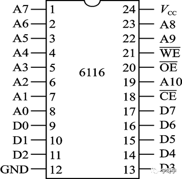
A10~A0: Address lines.
D7~D0: Data lines.
CE: Chip select signal.
OE: Data output enable signal.
WE: Write selection signal.
VCC: Power supply (+5 V).
GND: Ground.
2. Data Memory Expansion Connection
The data memory expansion connection is identical to that of program memory expansion regarding data and address lines; however, the control signals differ. Data memory uses /RD and /WR as read/write selection signals.
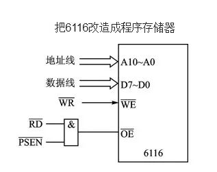
3. Using RAM Chips to Expand Read/Write Program Memory
RAM chips can be specially connected to serve as program memory, allowing both program execution and modification, effectively becoming a read/write program memory.
During program execution, the read signal for program memory /PSEN is required; while modifying the program, the read signal /RD and write signal /WR for data memory are used. Taking the 6116 chip as an example, the connection method for these three signals is illustrated in the circuit diagram below.
4. Characteristics and Usage of the 80C51 Microcontroller Memory System
1. Characteristics of the Microcontroller Memory System
(1) Coexistence of Program Memory and Data Memory
Program memory is required to store programs, while data memory is necessary for program execution. In the system, these two types of memory are completely separate, each having its own address space, operation instructions, and control signals.
(2) Coexistence of Internal and External Memory
On-chip memory is inherent to the chip, providing convenient access but limited capacity, which may not meet system requirements; external memory is system expanded. This results in a microcontroller system structure that includes both internal and external memory.
(3) Continuous Address Requirement for Program Memory
During programming, the addresses of internal and external program memory spaces must be continuous.
80C51 Memory’s 4 Physical Storage Spaces and 3 Logical Storage Spaces
2. Usage of the 80C51 Microcontroller Memory
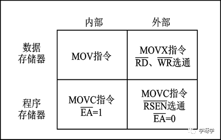
(1) Distinction of Storage Spaces
1) Distinction Between Internal Program Memory and Data Memory
The internal ROM and RAM of the chip are distinguished through instructions. The MOVC instruction is used to read ROM, while the MOV instruction is used to read RAM.
2) Distinction Between External Program Memory and Data Memory
For external expanded ROM and RAM, instructions are also used for distinction. The MOVC instruction is used to read external ROM, while MOVX instructions are used for reading/writing external RAM. /PSEN serves as the read selection signal for external ROM, while /RD and /WR serve as the read/write selection signals for external RAM.
3) Distinction Between Internal and External Data Memory
Internal RAM and external RAM are addressed separately, leading to an overlap in the addresses of the first 256 external RAM units. However, due to different instructions used for access, accessing internal RAM uses the MOV instruction, while accessing external RAM uses the MOVX instruction, thus preventing operational confusion.
(2) Interconnection of Internal and External Program Memory
To ensure continuous execution of programs, internal and external program memory must be uniformly and continuously addressed, using the same read instruction MOVC. The internal and external ROM face address interconnection issues. Considering that some chips in the 80C51 microcontroller series have internal ROM while others do not, the 80C51 microcontroller is specially configured with an EA (External Access Control) signal. The interconnection diagram is shown below.
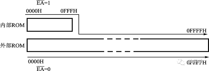
Interconnection Diagram of Internal and External Program Memory
From the above diagram, it can be seen that:
Since the storage space from 0000H to 0FFFH is occupied by internal ROM, external ROM cannot use this portion of storage space, resulting in a loss of 4 KB of storage space for external ROM.
For microcontrollers like the 80C31 that do not have internal ROM, /EA should be set to 0 (grounded). This way, only external ROM needs to be addressed, with the addressing range being 0000H to FFFFH, representing a complete 64KB ROM space.
Long press the image to follow
Discover more exciting content
WeChat ID : Mechanical-knowledge