Click the blue text to follow us

1. Microcontroller Measurement and Control System and Analog Input Channel
Measurement and control include two processes: “measurement” and “control”.
The so-called “measurement” is the real-time collection of physical parameters of the controlled object, such as temperature, pressure, flow rate, speed, and rotational speed. These parameters are usually analog quantities, i.e., continuously varying physical quantities.
The so-called “control” means that after processing the collected data through the microcontroller, conclusions are drawn to implement corrective control on the controlled object. However, the result obtained after microcontroller processing is a digital quantity.
The measurement and control system cannot do without the mutual conversion of analog and digital quantities; therefore, A/D (Analog to Digital) and D/A (Digital to Analog) conversion have become important components of the measurement and control system.
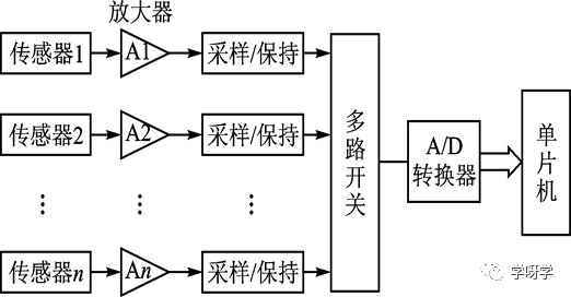
The operation of the analog input channel starts with signal acquisition. Since the amplitude of the analog signals collected by sensors is usually very small, and continuously varying signals are easily disturbed, the raw signals collected by sensors must be amplified, sampled, held, filtered, etc., before being sent to the A/D converter. This series of processing steps constitutes the analog input channel, as shown in the figure below.
The main function of the sensor is to collect signals, and it also has a signal conversion function, that is, it converts the collected non-electric signals into electrical signals (voltage or current) for subsequent processing. There are many types of sensors, and commonly used sensors include the following:
The voltage or current signals obtained from the sensors are often of small amplitude and difficult to perform A/D conversion directly, so amplifiers are needed to amplify the analog signals.
There are many types of amplifiers, but the type used in the analog input channel is a direct-coupled amplifier with high gain and deep negative feedback. Since it can perform various mathematical operations (such as proportional, addition, subtraction, integration, and differentiation) on the input signals, it is called an operational amplifier. Operational amplifiers have characteristics such as high input impedance, high gain, high reliability, low cost, and ease of use. There are now various specialized or general-purpose operational amplifiers available for selection.
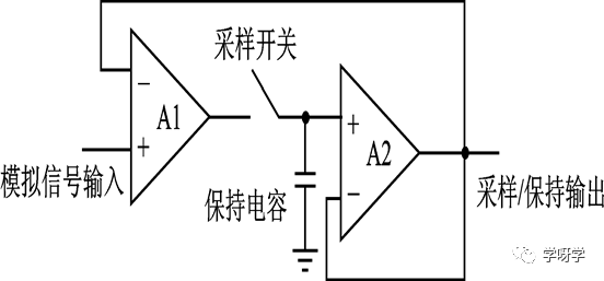
Sampling is to track the changes in the input signal, and its essence is to convert a continuously varying analog signal into a time-discrete sampled signal. The sampling frequency must be much higher than the highest frequency component in the analog signal (generally 2.5 times).
Holding is to maintain the sampled signal for a period of time, as the subsequent A/D conversion requires a time process. During the hold period, the signal must remain stable, and efforts should be made to keep the signal unchanged.
In the analog input channel, the sampling circuit and the hold circuit are combined, referred to as the sample/hold circuit. As shown in the figure below.
Filtering can be divided into analog filtering and digital filtering.
Analog filtering is completed by filtering circuits built with electronic components, and analog filtering can be divided into passive and active types. Passive filtering uses passive components (inductors, capacitors, and resistors) to construct filtering circuits. Active filters use amplifiers along with capacitors and resistors to construct filtering circuits.
Digital filtering involves smoothing the sampled signals through programs to enhance useful signals and eliminate or suppress interference signals. There are various digital filtering programs, such as program judgment filtering, median filtering, arithmetic mean filtering, weighted average filtering, first-order lag filtering, and composite filtering.
Compared with analog filtering, digital filtering has many advantages, which is why digital filtering is widely used in modern measurement and control systems. Digital filtering not only does not require hardware devices but is also very convenient to use; it only requires adding a segment of filtering program before entering data processing or control algorithms.
Many measurement and control systems are multiplex systems to facilitate multi-parameter collection. In a multiplex system, as long as the speed allows, a scheme should be adopted where multiple channels share a single A/D converter to simplify the structure and reduce costs. A multiplexer needs to be set up in the analog input channel to switch channels, allowing each channel to be connected in turn and alternately.
2. A/D Converter Interface
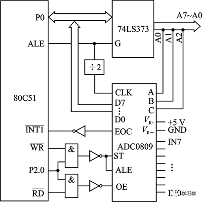
1. 8-bit A/D Conversion Chip and 80C51 Interface
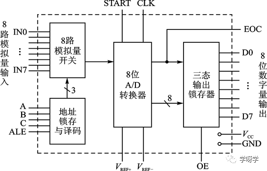
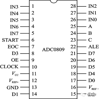
(1) ADC0809 Chip
ADC0809 adopts successive approximation A/D conversion principle and can achieve time-sharing collection of 8 analog signals. The chip has 8 analog switching gates and corresponding channel address latching and decoding circuits, with a conversion time of about 100 μs. The internal logic structure of ADC0809 is shown in the figure below.
-
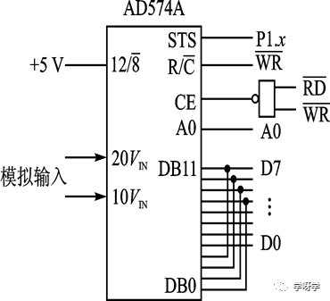
R/C: Read/start conversion signal. When R/C=0, it is the start conversion signal; when R/C=1, it is the read signal. -
STS: Conversion end signal. It is high during the conversion, and goes low when the conversion is complete. -
12/8: Output bit selection signal. When 12/8=1, it is a 12-bit output; when 12/8=0, it is an 8-bit output. -
CE: Enable signal, active high. It participates in controlling the start of conversion and reading data.
-
Integrating A/D Converter: Also known as dual-slope or multi-slope A/D converters. It is widely used and has advantages such as high accuracy and strong anti-interference ability. -
Successive Approximation A/D Converter: Simple principle, easy to implement, and does not have time delay problems. -
Flash A/D Converter: Its main feature is high speed, but it has high power consumption and complex circuits, so the chip size is also larger. -
ΣΔ A/D Converter: Also known as oversampling A/D converters. Although it appeared later, it has advantages such as high resolution, low cost, and strong anti-interference ability.
-
Unipolar voltage signals, all A/D conversion chips have this input form. The generally allowed voltage range is 0~+5 V, 0~+10 V, and 0~+20 V, etc. -
Bipolar voltage signals can be both positive and negative. Although they are still input through one lead, the chip needs a pair of power supplies with opposite polarities to work together. -
Differential signals are voltage signals that are not grounded together. Two polarities of differential signals require two signal lines to be input, represented on the chip as VIN+ and VIN-. Differential voltage signals can start from non-zero volts, with ranges such as ±2 V, ±4 V, ±5 V, and ±10 V.
-
The binary code A/D conversion chip outputs binary codes, with bit numbers ranging from 8 bits, 10 bits, 12 bits, 14 bits, 16 bits, 20 bits to 24 bits, etc. -
BCD code A/D conversion chips output multi-digit BCD codes. This type of conversion chip is typically used in digital voltmeters, where the output BCD code can be directly sent to LED or LCD for display. Common BCD code A/D conversion chips have bit numbers of 3.5 bits, 4.5 bits, and 5.5 bits, etc.
The A/D converter converts voltage, so its resolution is the ability to distinguish changes in the input voltage signal. The more bits the A/D converter has, the smaller the resolution value, and the stronger the resolution capability, meaning the converter’s sensitivity to changes in input quantity is higher. Therefore, when selecting an A/D converter, the number of bits should be given importance.
There are some control signals in A/D conversion chips, including clock signals, conversion start signals, and conversion end signals, etc. These signals need to be processed during interface connections.
The digital quantity data obtained after A/D conversion should be transmitted to the microcontroller for processing in a timely manner, and reading should be done after data conversion is complete.
3. D/A Converter Interface
There are many D/A conversion chips; here we take DAC0832 as an example.
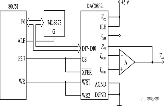
DAC0832 is an 8-bit D/A conversion chip powered by a single +5 V supply, with a reference voltage range of ±10 V, a current settling time of 1 μs, using CMOS technology, low power consumption (20 mW), and a 20-pin dual in-line package. The pin arrangement is shown in the figure below.
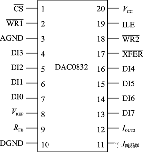
-
DI7~DI0: Data input for conversion.
-
CS: Chip select signal (input), active low.
-
ILE: Data latch enable signal (input), active high.
-
WR1: First write signal (input), active low.
-
XFER: Data transfer control signal (input), active low.
-
WR2: Second write signal (input), active low.
-
IOUT1: Current output 1. When the data is all 1s, the output current is maximum; when all 0s, the output current is minimum.
-
IOUT2: Current output 2.
-
RFB: Feedback resistor terminal, which is the feedback resistor terminal of the operational amplifier, and the resistor (15 kΩ) is fixed in the chip. DAC0832 is a current output type D/A converter; to obtain voltage conversion output, operational amplifiers need to be connected to the two current output terminals, with RFB being the feedback resistor of the operational amplifier.
-
VREF: Reference voltage, an external high-precision voltage source connected to the internal resistor network of the chip. This voltage can be positive or negative, with a range of -10 to +10 V. The reference voltage determines the output voltage range of the D/A converter; for example, if VREF is connected to +10 V, the output voltage range is 0 to -10 V.
-
DGND: Digital ground.
-
AGND: Analog ground.
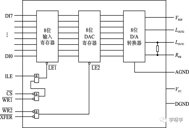
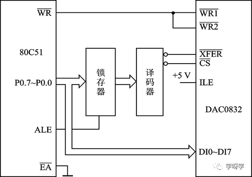
The internal structural block diagram of DAC0832 is shown in the figure below, where the resistor decoding network is included in the 8-bit D/A converter shown in the diagram. The input channel consists of an input register and DAC register, forming two levels of data input latching, controlled by three “AND” gate circuits to produce LE1 and LE2 signals, which control the two input registers.
2. Single Buffer Connection Mode for DAC0832
3. Dual Buffer Connection Mode for DAC0832
The so-called dual buffer connection mode means that both the input register and DAC register of DAC0832 are connected in a controlled latching mode. In multi-channel D/A conversion, if synchronous output is required, the dual buffer connection mode should be used. The dual buffer connection mode for DAC0832 is shown in the figure below.
4. Serial Interface of A/D and D/A Converter Chips
For A/D or D/A conversion chips with I2C bus interfaces, the interface can be realized through the I2C bus. Here, we take the mixed chip PCF8591 as an example.
PCF8591, produced by Philips, is a typical mixed A/D and D/A conversion chip with I2C bus interface, using CMOS semiconductor technology. The analog input channel of the A/D conversion part has 4 channels, with a conversion result of 8 bits, adopting a successive approximation conversion method with a sample/hold circuit. The D/A conversion part has 1 analog output. The pin arrangement of the dual in-line chip is shown in the figure below.
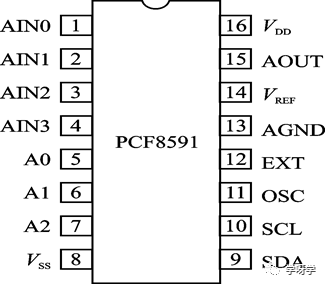
- AIN3~AIN0: Analog signal input.
- A3~A0: Pin addresses.
- SCL, SDA: I2C bus interface signals.
- OSC: External clock input, internal clock output.
- EXT: Internal/external clock selection, EXT=0 selects internal clock, EXT=1 selects external clock.
- Aout: D/A conversion analog output.
- VDD, VSS: Chip power supply.
- VREF: Reference power supply.
- AGND: Analog ground.
- PCF8591’s device address is 1001, and the pin address is set by A2, A1, and A0. A system can expand up to 8 PCF8591 chips.
- PCF8591 has a control register inside, and the microcontroller controls A/D and D/A conversion by writing control words to this register. Therefore, before conversion, it is necessary to transmit the control word.
- The main content of the control word written during D/A conversion in the PCF8591 chip is to set the analog output enable bit to 1. Subsequently, each time a data byte is written, the conversion result is output at the AOUT terminal.
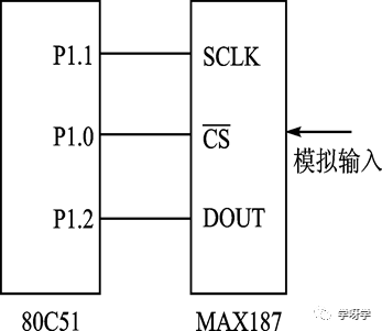
For microcontroller chips without a serial interface, a software simulation method can be used to achieve a serial interface. Taking MAX187 as an example. MAX187 is a 12-bit single analog channel A/D conversion chip with an SPI bus, which has a sample/hold circuit and adopts a successive approximation conversion method with a conversion time of 10 μs. The pin arrangement is shown in the figure below.

- AIN: Analog signal input, effective voltage range is 0 V~VREF.
- DOUT: Serial output of conversion results.
- SCLK: Clock signal input.
- CS: Chip select signal.
- SHDN: Control signal. This pin is connected to low level, and the chip is in low power mode; this pin is connected to high level, and the chip uses the internal reference power supply; this pin is left floating, and the chip uses the external reference power supply.
- VREF: Reference power supply.
- VDD: Chip power supply.
- GND: Digital ground and analog ground.
The connection of the software simulated serial interface is very simple; just connect three port lines of the 80C51 to the CS, SCLK, and DOUT signal pins of MAX187, as shown in the figure below.

Long press the image to follow
Discover more exciting content
WeChat ID: Mechanical-knowledge