 The biggest challenge in high-speed design is to minimize crosstalk, ensuring good signal integrity during transmission while also reducing the impact of noise on the PCB. Since single-ended signals and Low Voltage Differential Signaling (LVDS) are typical types of high-speed interface signals, it is essential to ensure the transmission of these two types of signals.In most cases, the recommendation to avoid such issues is to follow design guidelines, but designers must weigh various design principles during the design process. Designers must decide on parameters that will affect performance, reliability, and design costs.Because designers need to consider and keep the above issues in mind, special attention must be paid to the following key aspects during the design process.
-
Selection of high-speed PCB layers
-
Layout of signal transmitting and receiving components.
-
Impedance control during routing.
-
Wiring of high-speed serial signals.
-
Termination correction at transmission line ends.
-
Minimization of crosstalk between signal channels.
-
PCB level filtering and decoupling.
Design of High-Speed PCB Layer Stacking StructureAt the beginning of the PCB design, it is crucial to correctly select the hierarchical structure of the high-speed PCB, as different hierarchical structures can affect routing paths and impedance control. Impedance control during routing is one of the main parameters in high-speed design.The following conditions must be considered:
-
How to ensure a fixed GND reference voltage on high-speed lines while maintaining impedance continuity;
-
Signal lines must have a minimum spacing to the reference plane layer;
-
Maximize the capacitive reactance of the power domain layer;
-
How to reduce vias or layer transitions for high-speed signals.
Since decoupling capacitors on discrete PCBs only work effectively at signal frequencies up to 200MHz, it is advisable to use plane layer decoupling whenever possible.By adopting a stacked design structure, a power plane layer capacitor can be built, which has decoupling effects at high frequencies, becoming effective at frequencies above 200MHz.The following are examples of the stacking structure design for 4-layer and 6-layer PCBs.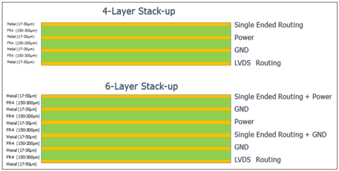 Figure 1. Example of 4-layer and 6-layer PCB stacking structure designComponent Layout
-
First, place the MCU and connectors that use high-speed signal connections, ensuring the routing path between them is the shortest distance.
-
Do not place other components between the connector and the MCU.
-
Keep potential noise sources away from high-speed signals.
-
Place components that communicate with other devices outside the PCB at the edge of the PCB.
Table 1. Considerations when “Output, Power, Input, and I/O” pins are not in use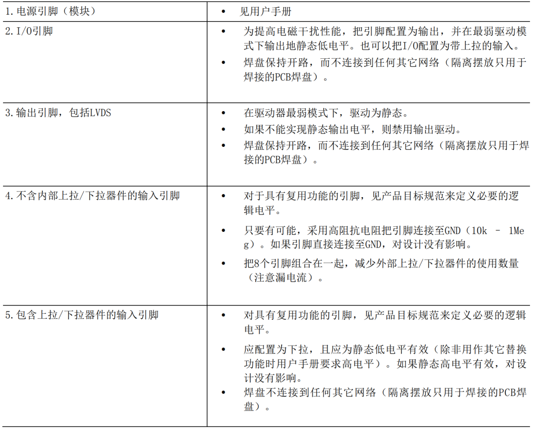 Impedance Control Design During RoutingOne of the key issues to ensure high-speed signal transmission is routing design. The routing impedance design is 50 ohms, and the differential impedance for LVDS signals is 100 ohms.There are two types of transmission lines that can be used for routing design:
-
Microstrip
-
Stripline
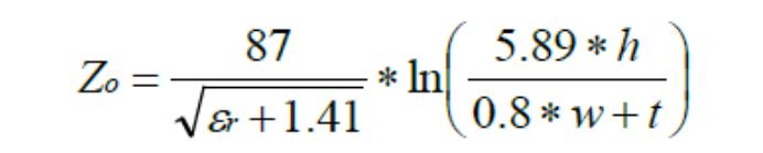
Based on the selected hierarchical design scheme, calculate the characteristic impedance of the microstrip or stripline transmission line to achieve a routing impedance of 50 ohms.Microstrip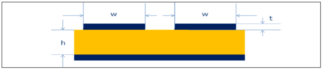 Figure 2. Microstrip transmission lineFormula:
 Stripline
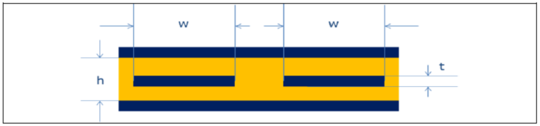 Figure 3. Stripline transmission lineFormula:
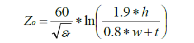 Key values in the formula:
- h
- For microstrip calculations = height to ground
- For stripline calculations = distance to ground
- w = routing width
- t = line thickness
- εr = relative permittivity of the substrate (all distance units in inches)
Transmission Line ParametersUse transmission line parameters to calculate routing impedance. Parameters are provided by the PCB manufacturer.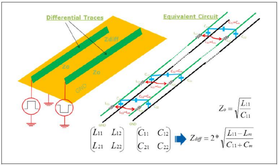 Figure 4. Calculating impedance using transmission line parametersTo determine whether routing should be considered as controlled impedance routing (critical length), the following rules and calculation formulas should be followed—If the routing length is longer than 1/4 of the distance traveled during the signal rise time, impedance control should be applied.Simple calculation (for FR4 material and 500ps rise time):Propagation speed:
 Rise time distance:
 Critical length:
 From the perspective of suppressing electromagnetic interference (EMI), it is recommended to use stripline, as they are placed in the inner layers, and routing will not cause radiation outside the PCB.However, stripline requires layer transitions, which can lead to impedance discontinuities and reflections. Due to the presence of different reference planes, it is challenging to meet the requirements for 50 ohm routing impedance and 100 ohm differential impedance.Differential impedance is defined based on the following values:
-
Distance between lines
-
Distance to reference plane
To accurately calculate routing and differential impedance, a 2D field solver or signal integrity function in layout design tools can be utilized. Most tools on the market provide such functionality. This way, when designing the routing path, there is no need to worry about impedance calculations, as the tools can assist in calculating and adjusting the relevant parameters to ensure that routing is always controlled for impedance.When designing and connecting routing, follow the rules below:
-
Use the widest routing possible.
-
It is recommended to use microstrip, as differential signals will cancel most of the emissions.
-
If there are still emission issues, stripline can also be used.
-
Keep the routing width/spacing ratio less than 0.8 to reduce the impact on routing impedance.
-
The PCB manufacturer should ensure that 50 ohm routing and 100 ohm differential impedance are within ±10% tolerance.
Routing Width EstimationIn the early design phase, use the following flowchart to estimate routing width, and then calculate impedance.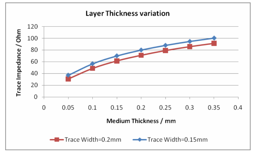 Figure 5. Routing impedance variation with layer thickness
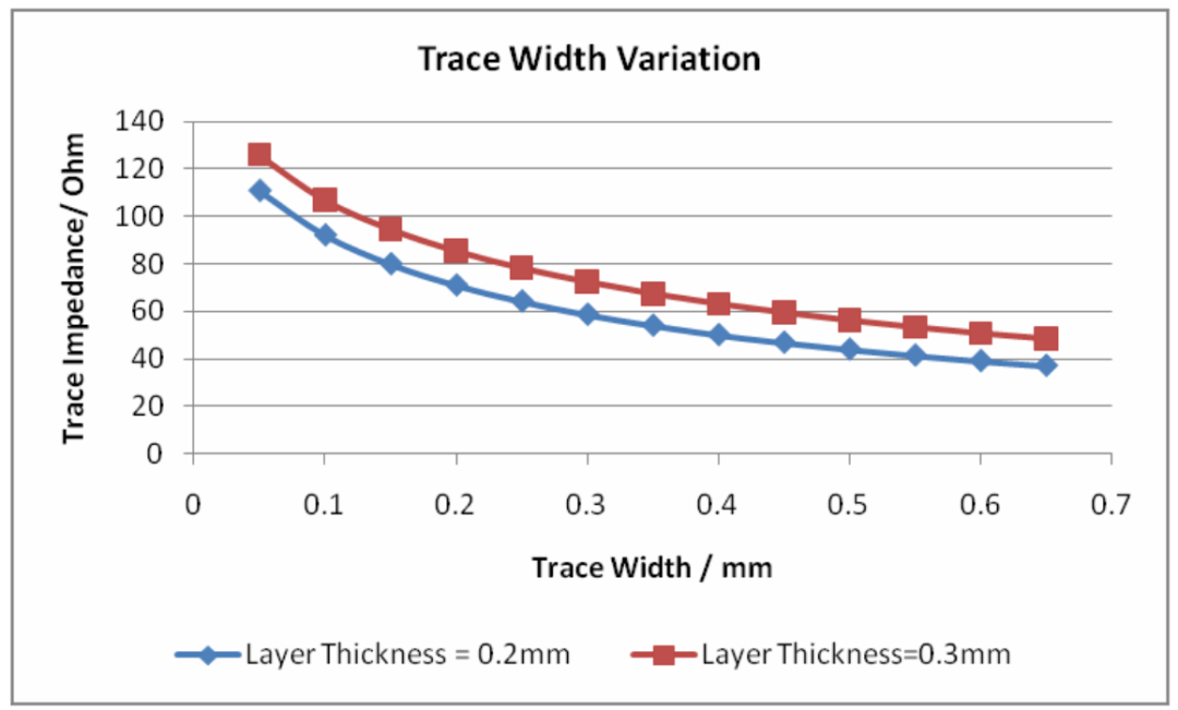 Figure 6. Routing impedance variation with routing width
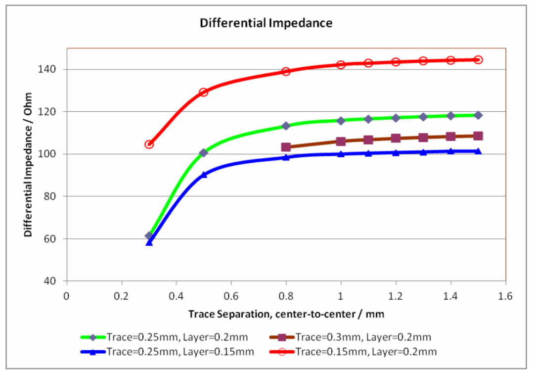 Figure 7. Differential impedance variation with routing separationWiring of High-Speed Serial Signals
-
First, high-speed signals should be prioritized in routing to meet impedance continuity requirements, with short distances and optimized channel designs.
Do not place routing on separation layers. Routing should be continuous, with a solid reference GND plane throughout its length to avoid impedance discontinuities and reflections.
-
Remember, the return current path should be close to the signal line. Keep the current loop as small as possible.
-
Keep routing as short as possible.
-
Arrange routing to be straight. Differential lines require point-to-point connections, avoiding daisy chain routing. If daisy chain routing is necessary, do not use short stubs in the daisy chain connections.
-
If unavoidable, use 45-degree bends instead of 90-degree bends.
-
Avoid layer transitions and vias in routing.
-
If layer transitions are unavoidable, use GND reference.
-
If layer transitions are unavoidable, place GND vias close to the signal lines (differential vias – GSSG).
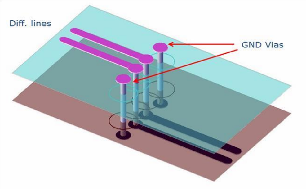 Figure 8. Differential vias
-
All differential routing must match in length.
-
Different lengths of differential routing can lead to skew between differential pairs. Skew can affect common mode and increase voltage jitter.
-
For Gb/s interfaces, the length difference of differential routing should be less than 1mm.
-
Route single-ended lines on different layers as differential pairs, or maintain a minimum distance of 4 line widths between them to reduce crosstalk.
-
Avoid impedance discontinuities in routing.
-
Reference to GND plane AC coupling capacitors SMT pads will have different impedance values than the required 50 ohms. In this case, the GND layer under the pad can be removed, but it must be ensured that the field solver is analyzed based on the impedance result values.