Abstract: This article introduces the composition, working principle, and remote configuration of the FPGA remote experiment system, focusing on the principle and specific implementation of remote configuration in the FPGA remote experiment system. Under the guidance of the ARM microcontroller, FPGA configuration data is transmitted and downloaded via Ethernet, and then the ARM acts as a timing controller to complete the FPGA remote configuration through the slave serial configuration method of FPGA. During the FPGA configuration, the output waveform of the configuration pins is studied to verify the configuration principle in the slave serial configuration mode.
1 Introduction
In recent years, the use of programmable devices such as FPGA/CPLD and VHDL for hardware design has developed rapidly. Programmable logic devices have gradually replaced traditional general-purpose medium and small-scale integrated circuits and have been widely applied. As the complexity of systems increases, the use of EDA (Electronic Design Automation) software, which plays an important role in the development of electronic systems, has made FPGA the preferred method for experimental teaching in courses such as digital logic circuit design, computer architecture, and embedded systems. With the development of embedded technology and network technology, remote control has become easier to implement. By introducing remote control technology into FPGA experimental systems, the reprogrammable nature of FPGAs can be utilized to achieve remote execution of FPGA experimental operations, thereby enabling remote sharing of experimental equipment and maximizing the utilization of experimental devices.
2 FPGA Working Principle and Configuration
The Field Programmable Gate Array (FPGA) is a product that has further developed based on programmable devices such as PAL, GAL, and CPLD. It emerged as a semi-custom circuit in the field of Application-Specific Integrated Circuits (ASIC), solving the shortcomings of custom circuits and overcoming the limitations of the number of gate circuits in traditional programmable devices. Circuit designs completed using hardware description languages (Verilog or VHDL) can be quickly programmed onto the FPGA for testing through simple synthesis and layout, making it the mainstream technology for modern IC design verification.
FPGA uses small lookup tables (16×1 RAM) to implement combinatorial logic, with each lookup table connected to the input of a D flip-flop, which then drives other logic circuits or I/O, thus forming the basic logic unit module that can realize both combinatorial logic functions and sequential logic functions. These modules are connected to each other or to I/O modules using metal wiring. When the FPGA is working normally, the configuration data is stored in SRAM cells, also known as Configuration RAM. Since SRAM is volatile memory, external circuits need to reload the configuration data into the internal configuration RAM after the FPGA is powered on. The FPGA configuration process is as follows: the external circuit loads the configuration data into the internal configuration RAM; the configuration data in the internal configuration RAM is used to control the initialization of the FPGA’s programmable internal logic, internal registers, I/O register enabling, etc. After configuration is complete, the FPGA enters user mode. After power loss, the FPGA reverts to a blank state, and the internal logic relationships disappear.
There are generally four configuration modes for FPGA: Slave Serial, Master Serial, Slave Parallel/SelectMap, and Boundary Scan mode. The selection of the configuration mode is generally determined by the input levels of the configuration mode selection pins on the FPGA chip.
Slave Serial configuration mode refers to the process where the external controller dominates the synchronous clock input during configuration, loading the configuration data bit by bit into the FPGA. Master Serial configuration mode, under the action of the FPGA’s internal synchronous clock, serially loads the configuration data from external memory into the FPGA bit by bit. Slave Parallel mode allows multiple bits of configuration data to be input in parallel. Boundary Scan mode, also known as JTAG configuration mode, is used during the development and debugging phase.
3 ARM-Based Remote Experiment System
The main function of the ARM-based remote experiment system is to enable remote FPGA experimental operations. Users can log into the experiment system on the PC side to schedule FPGA experiments, send FPGA control commands, and receive experimental result information. The system structure, as shown in Figure 1, is mainly divided into three modules: PC client, server, and ARM-FPGA module. The PC client provides users with a remote experiment operation interface, the server is primarily responsible for sending and receiving data or commands, while the ARM-FPGA module controls and executes the commands sent from the client and returns experimental results to the server.

3.1 PC Client
The main role of the client is to provide a user operation interface, allowing users to control the FPGA configuration and related FPGA experimental operations remotely. The client is primarily designed using C/C++ programming and employs a socket programming model to send configuration data and return configuration result data.
3.2 Server
The server is the core of the remote experiment system based on the FPGA experimental platform, responsible for controlling the operation of the experiment system. It manages the scheduling of the FPGA experimental platform, assigning idle experimental platforms to experimental users (PC clients). Moreover, it needs to connect to hundreds of ARM clients and PC clients, acting as an information relay station between the two types of clients. Additionally, the server manages the database, promptly recording and updating information related to students, FPGA platform, reservation records, and experimental records.
3.3 ARM Client
The ARM client, as an important component of the overall system structure, is the only interface for data interaction with the FPGA experimental platform. It mainly implements the following functions:
(1) Connect to the server, receive command information from the PC client, and also receive the stored FPGA configuration execution files.
(2) Parse commands and call programs to complete the commands.
(3) Implement dynamic configuration of the FPGA, loading the configuration files for execution on the FPGA.
(4) Connect to the PC client, sending relevant pin information of the FPGA in real-time.
(5) Implement remote control operations for switches and buttons on the FPGA experimental platform.
4 Implementation of FPGA Remote Configuration
In this experiment, an ARM9 development board and FPGA experimental board are used to achieve the specific implementation of FPGA remote configuration. The ARM controller uses a microcontroller development board with ARM9 as the processor. The ARM9 development board supports network interface connections and has successfully ported the Linux 2.6.30 kernel operating system and the corresponding file system, providing a good Linux environment for socket network programming and software implementation and execution of the ARM client. The FPGA uses an FPGA experimental board designed for computer architecture, with the FPGA chip being the Spartan-6 series produced by Xilinx, and its specialized configuration interface is brought out for subsequent experimental operations.
4.1 Configuration File
The configuration data format used for the FPGA in this design is the .bin format, which is a format for FPGA configuration data generated by Xilinx’s FPGA design tool ISE software, and is also the format for serial configuration data for Spartan-6 series chips. On the PC client, configuration pins can be set up through socket programming.
Transmit the file over the network to the ARM controller client.
4.2 Configuration Circuit
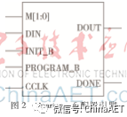
The Spartan-6 configuration pins are shown in Figure 2, and the functions of each pin are described in Table 1. Table 1 FPGA Configuration Pin Description
Pin Name Type Description
M[1:0] Input Mode selection pins that determine the FPGA’s configuration mode
CCLK Input/Output Synchronous clock source for all configuration modes except JTAG
DIN Input Serial configuration data input pin, synchronized to the rising edge of the clock
DOUT Output Used for Daisy Chain configuration data input for subsequent devices
DONE Output High level indicates configuration is complete, low level indicates configuration failed
INIT_B Input/Output Pulling this pin low before configuration mode selection indicates delayed configuration; after mode selection, the level output indicates whether CRC check errors occurred:
0=CRC error
1=No CRC error
PROGRAM_B Input Low level input to reset the chip
4.3 Configuration Process
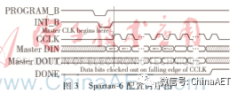
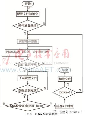
The configuration timing of the Spartan-6 chip is shown in Figure 3. First, provide a low-level signal to the PROGRAM_B pin, then restore it to high level, and check the INIT_B pin level signal. If the level signal changes with PROGRAM_B, it indicates that the FPGA internal configuration has been initialized and can proceed with FPGA configuration. Next, under the signal synchronization of the DCLK pin input to the FPGA by the ARM, the configuration data is loaded bit by bit until all configuration data is loaded. When the DONE pin signal changes to high level, it indicates that the FPGA configuration is complete, and it enters operational status. The flowchart of the configuration program is shown in Figure 4.
5 Experimental Results Analysis
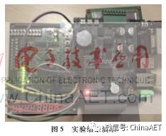
During the experiment, the FPGA configuration pins DIN, CCLK, INIT_B, DONE, and PROGRAM_B are connected to the I/O pins of the ARM development board. It is also important to ensure that the ARM development board and FPGA experimental board share a common ground. After connecting the ARM development board to the network cable, powering it on, and starting it up, the configuration file is transmitted and loaded via the PC client. When the configuration is complete, the client receives “config done!” indicating that the configuration is complete. The experimental results demonstration is shown in Figure 5.
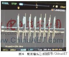
To obtain the data from the DIN and CCLK pins during the configuration process, configuration data output was performed in the program, and the output waveforms of these two pins were captured using an oscilloscope, as shown in Figure 6. It can be seen from the figure that in one configuration cycle, the ARM controller performs bit transmission by byte, with each byte consisting of 8 bits of data. During each clock input, one bit of configuration data is input until all configuration data is loaded, completing the FPGA configuration.
6 Conclusion
This design employs the connection of two independent modules to achieve the overall functionality, and some command operations of the ARM controller are transmitted via serial ports. In the upcoming FPGA remote experiment system, all command operations of the ARM will be fully implemented through a single network cable, enabling not only remote configuration of the FPGA but also remote experiments—remote FPGA experiments that are real on the remote side and virtual on the local side. This means that operations such as switches and buttons on the client computer will be completed on the interface, and these command operations will be transmitted via the network cable to the ARM side, controlling the input high and low levels of the relevant FPGA pins, and returning the output levels of the relevant pins, which will be displayed on the client computer through LEDs or digital tubes.
References
[1] Ding Wei, Xiao Tiejun. Design and Implementation of a General Experimental Platform Based on FPGA. Wireless Communication Technology, 2013, 22(4):38-39.
[2] Liu Xiaolei, He Guangping. Configuration and Downloading of FPGA Chips. Science and Technology Information, 2011(15):109-109.
[3] Gao Chuang, Wu Lihua, Fang Luo, et al. Design of a Configurable Memory for FPGA. Research and Progress in Solid State Electronics, 2016, 36(1):67-67.
[4] Chen Xi, Shen Zuofeng. A Reliable Dynamic Configuration Method for FPGA and Its Implementation. Communication Technology, 2012, 45(3):105-107.