1. Introduction
In the previous article, we extracted the firmware of the smart lock through the SWD interface and successfully loaded it using IDA. This article will continue analyzing the firmware, studying how the lock processes the communication data of BleKey sent by the phone via BLE.
Continuing from the previous article, we followed the processing method of the Guojia lock firmware to analyze the Lock’s firmware, and the navigation bar of IDA is shown in the figure below.

Figure 1-1 Navigation bar after directly parsing the firmware in IDA
As seen in the image, currently, only a small part of the firmware has been parsed into code, while the vast majority of the firmware data remains in unexplored status. By browsing the strings in the firmware, we can find the content shown in the image below:
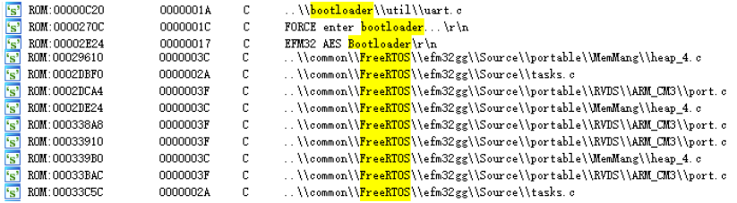
Figure 1-2 Some strings in the firmware
Combining the successfully parsed code snippets, we can speculate that this part of the code is merely the bootloader, and the subsequent main program may have used the FreeRTOS system (an open-source real-time operating system, https://www.freertos.org/).
Given the current situation, we can choose to directly “dive in,” starting the analysis from the bootloader all the way to the BLE processing flow. However, since the lock firmware uses the FreeRTOS operating system, this analytical approach will be a bit more complicated. Here, we can choose a more straightforward research method: since the lock circuit board has provided SWD pins, let’s see if we can “take a shortcut” and quickly locate the key positions in the firmware through SWD debugging. We will share the analysis methods for bootloader and FreeRTOS in a subsequent special article.
2. SEGGER JLink Debugging Functionality
Before debugging, let’s briefly introduce how to use the debugging functionality of SEGGER JLink (hereinafter referred to as JLink). In the previous article, we used the command line tool of JLink to extract the firmware. This command line tool also includes instructions for setting breakpoints, pausing the CPU core, reading/writing registers or specified memory locations, single-step debugging, and other dynamic debugging needs. Specific details can be found in SEGGER’s Wiki (https://wiki.segger.com/J-Link_Commander). You can choose to use openOCD in conjunction with JLink for debugging, but we will not introduce openOCD in this article and will instead choose another debugging tool.
In practical debugging, the command line tool usually needs to be used in conjunction with IDA, which can be cumbersome and the information displayed is not intuitive enough. SEGGER provides a graphical interface tool—Ozone, which can somewhat alleviate the above problems. For an introduction to Ozone, you can refer to SEGGER’s official website (https://www.segger.com/products/development-tools/ozone-j-link-debugger/), where you can also find the software and user manual download page. After downloading, the installation can be completed by clicking next, which I believe everyone is quite familiar with (humorously).
After installation, you can create a new project by selecting “File->New->New Project Wizard”. During the creation, you need to select the model of the chip to be debugged, the type of debugging interface, communication rate, and other information. Continue by clicking “Debug->Start Debug Session->Attach to Running Program” to connect to the device to be debugged. Note that the computer, debugger, and device must remain connected throughout the debugging process, as shown in the image below.
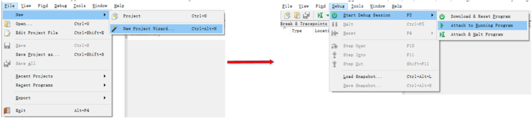
Figure 2-1 Connecting to the device
After connecting to the device to be debugged, Ozone can display multiple subviews like IDA, allowing for the simultaneous observation of various information. The image below shows the interface I used during a debugging session.
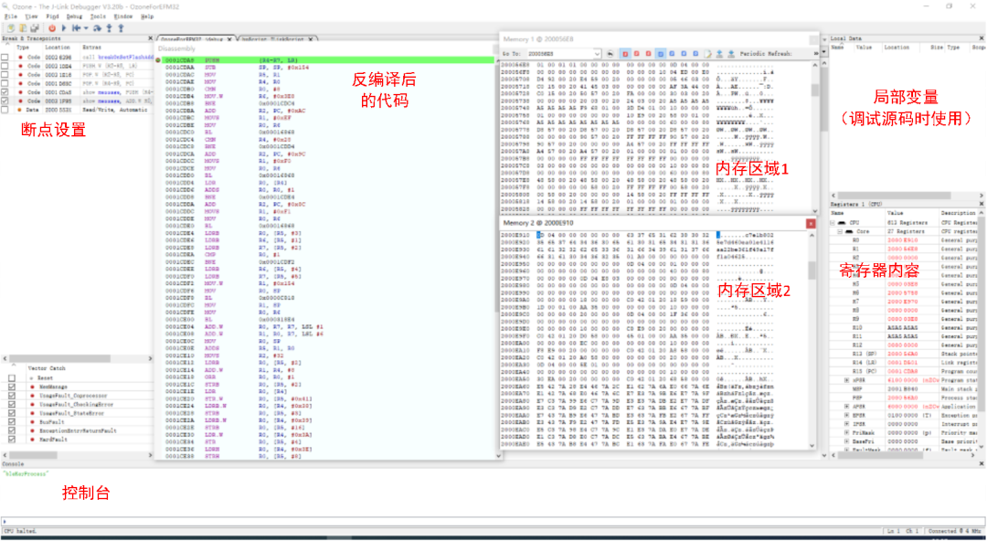
Figure 2-2 Ozone Debugging Interface
As shown in the image, during debugging, we can see the data of the registers, the data of multiple memory areas, and the disassembled code all at once. The console area below can execute some instructions or pre-written scripts. Additionally, in the upper left corner of the breakpoint setting area, we can see that besides Location, the breakpoint has two other attributes: Type and Extra. By reading the user manual, we can determine that these two attributes are used to set the breakpoint type, such as execution breakpoints, read/write breakpoints, TRACE breakpoints, etc., as shown in the image below:
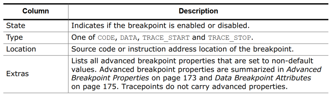
Figure 2-3 Breakpoint Attributes in Ozone
Ozone also provides many powerful functions, which we will introduce one by one when we use them later.
3. Debugging the Lock via SWD Interface
Having learned the basic usage of Ozone, let’s debug the lock firmware. Reviewing the first analysis article on the Lock, we analyzed the communication data between the Lock and the mobile app and learned that BLE communication is protected by AES encryption. Reflecting on the analysis article of the Guojia lock, we used constants from the TEA encryption to locate the communication handling code of the lock, so can we also start from AES encryption here?
3.1 AES Encryption and Decryption in the Firmware
Looking through the chip manual of the lock’s MCU, we can see that the chip provides an AES processing module, and the memory mapping of this module is shown in the image below.
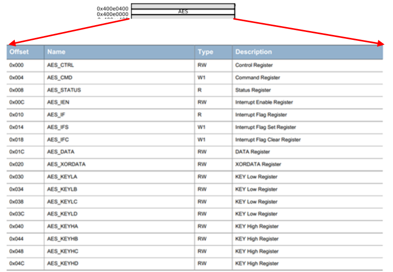
Figure 3-1 Memory Mapping in EFM32
Clearly, we assume that the Lock uses the chip’s AES module for encryption and decryption operations instead of writing the AES algorithm from scratch, which means it must access the memory addresses in the range of 0x400E0000~0x400E0400. Therefore, we just need to set appropriate read/write breakpoints and wait for the phone to communicate with the lock to trigger the breakpoints.
In the breakpoint setting area, right-click and select Set Data Breakpoint, a window will pop up as shown in the image below.
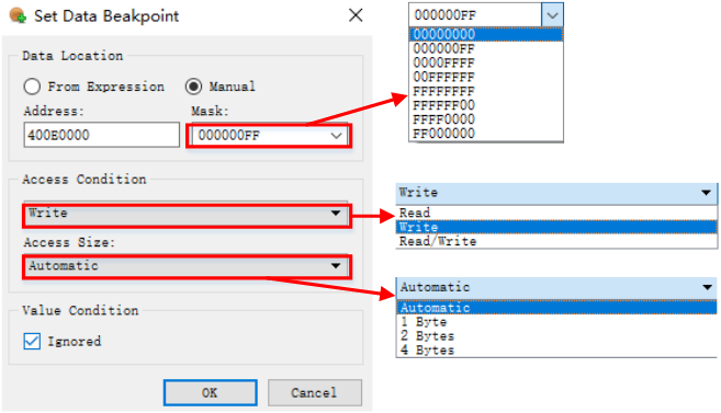
Figure 3-2 Setting Data Breakpoint
The settings in the image indicate that a breakpoint will be triggered when the CPU writes data to the address 0x400E00XX.
After setting the breakpoint, click to unlock on the phone. Since the data breakpoint we set monitors a memory area, it will be triggered multiple times during the unlocking process. Later, we can see a small section of code on the left side of the image, and on the right side is the register data when executing at address 0xED0C.
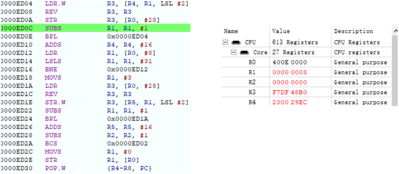
Figure 3-3 Breakpoint for Writing Data to be Decrypted
In the image, the address 0x400E001C (R0 + 28) is the AES_DATA register, and this small section of code is writing data to the AES_DATA register, which should be the AES processing function (hereinafter referred to as AESFunc). By backtracking the call stack, we can find the outer function that calls AESFunc and the starting address of the AESFunc function, and then use IDA’s F5 function to analyze the AESFunc function, as shown in the image below:
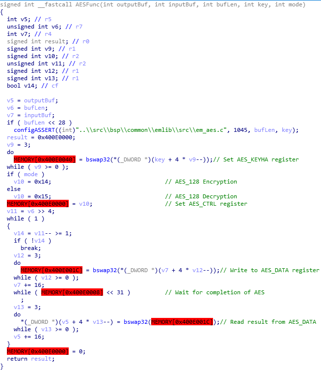
Figure 3-4 Pseudocode of AESFunc Function
Combining with the chip manual, it is easy to determine the function of each parameter of AESFunc from the pseudocode. In the first article of this series, we learned that the decryption key during unlocking is the BleKey, and the process of obtaining the lock’s BleKey is that the server sends a set of data, totalData, to the mobile app, which forwards it directly to the lock via BLE without any processing. Next, let’s take a look at how the lock processes totalData.
3.2 The Process of the Lock Obtaining BleKey
First, we need to look at what the content of totalData is, as shown in the image below:
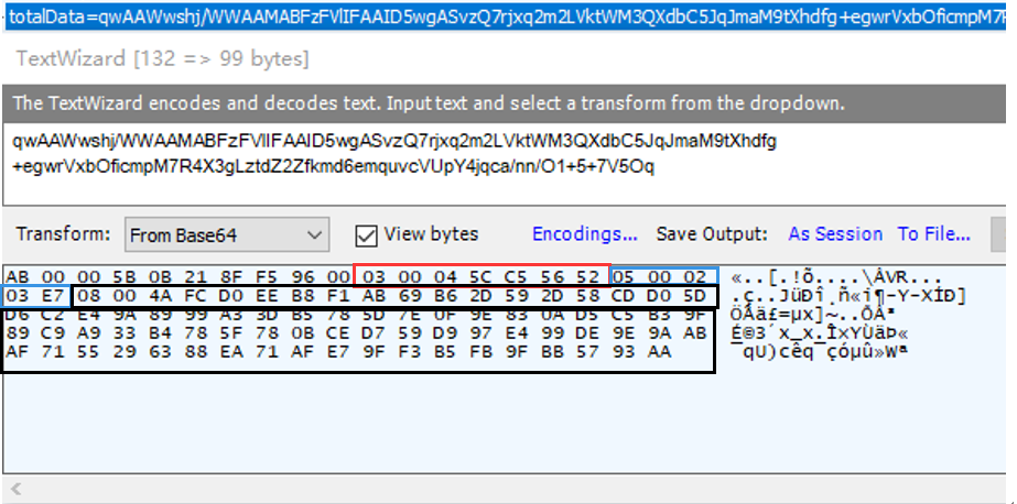
Figure 3-5 totalData Field and Its Base64 Decoded Data
We can see that totalData is a string of binary data encoded in base64. The part before the red box can be viewed as the header of the data, containing the message header, data packet sequence number, checksum, etc. The body part after the header, i.e., the data in the red, blue, and black boxes, has the same structure for the three groups of data, as shown in the image below:

Figure 3-6 Data Structure Used in totalData Payload
The data_type of 0x03 in the red box has a data_content of 0x5FFFECAE, which is related to the AES root key ciphertext. The body of totalData has two more sets of data, the specific function of which will not be elaborated here as it is somewhat inappropriate to discuss too much.
Next, we set a breakpoint at the entry of AESFunc and can see the value of BleKey as shown in the image below:

Figure 3-7 BleKey in Memory
From Figures 3-5 and 3-7, we cannot see the connection between BleKey and totalData. Presumably, there is some decryption or decoding transformation between the two, so we need to continue searching for the lock’s processing of totalData. Keeping the breakpoint in the AESFunc function, we can discover that totalData is also decrypted through the AESFunc function during debugging. At this point, backtracking the call stack can reveal the key code as shown in the image below.
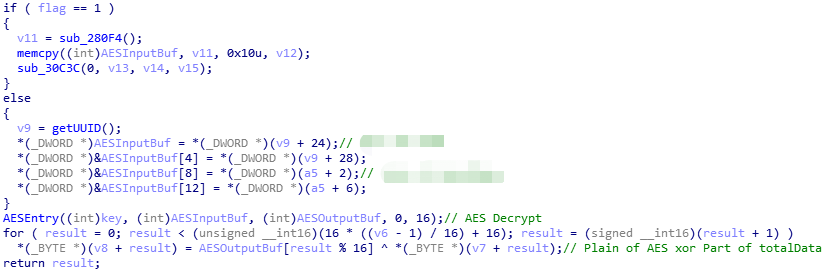
Figure 3-8 Processing of totalData
The AESEntry function in the image is a wrapper for AESFunc; this part is the core code that generates BleKey from totalData. The process can be organized as shown in the image below.
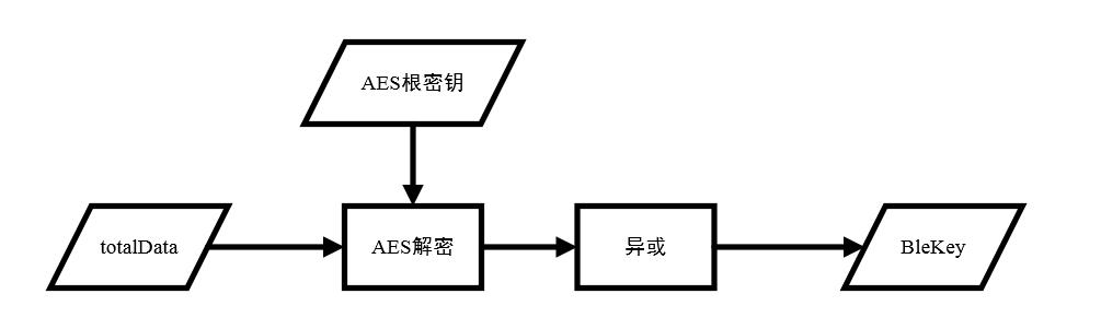
Figure 3-10 Flowchart of BleKey Acquisition
In this process, without the root key, it is impossible to decrypt and obtain BleKey. Through debugging, we can find that the storage address of the root key in Flash is 0x7E09C.
4. Conclusion
The series of articles on the Lock ends here. We will not discuss the logic of other functions in detail; interested readers can explore on their own. In the first article about the Lock, we learned through reverse engineering the mobile app that the Bluetooth communication data of the lock has AES encryption protection. The second article shared how to use the SWD interface to extract the firmware. This article further analyzes the process of the lock obtaining BleKey through debugging the lock firmware. In the next special article, we will introduce other analysis techniques regarding the Lock, but we will not discuss the operating logic of the Lock any further. Interested readers please stay tuned for our subsequent articles. Finally, I hope everyone gains something from this.
Light & Yimi Hu @ PwnMonkeyLabs
Click the “Read the Original” button below to enter the topic and view the series of articles.