Silicon materials are divided into monocrystalline silicon and polycrystalline silicon based on the arrangement of their crystal cells. The main difference between monocrystalline and polycrystalline silicon is that the crystal cell arrangement in monocrystalline silicon is ordered, while that in polycrystalline silicon is disordered. In terms of manufacturing methods, polycrystalline silicon is generally made by melting silicon material directly in a crucible and then cooling it. Monocrystalline silicon is formed by pulling a single crystal to create a crystal rod (the Czochralski method). In terms of physical properties, the characteristics of the two types of silicon differ significantly. Monocrystalline silicon has a higher conductivity and a higher photoelectric conversion efficiency, typically around 17% to 25%, while polycrystalline silicon has an efficiency of less than 15%.
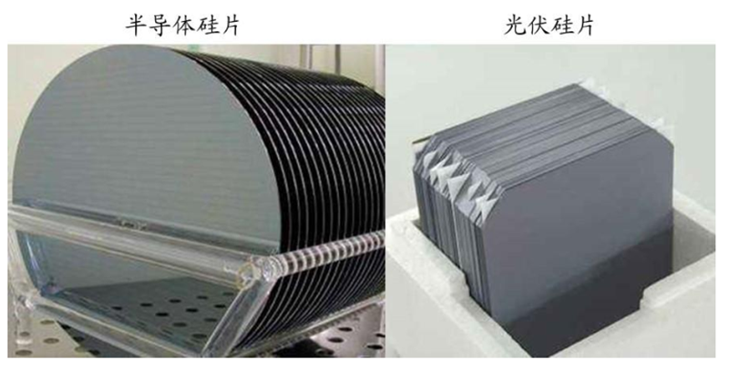 ▲ Semiconductor silicon wafers and photovoltaic silicon wafers
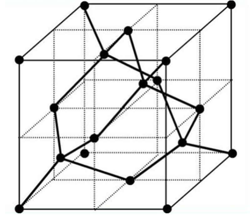 ▲ Monocrystalline silicon crystal cell structure
Photovoltaic silicon wafers: Due to the photoelectric effect and the clear advantages of monocrystalline silicon, silicon wafers are used to convert solar energy into electrical energy. In the photovoltaic field, the typical shape used is rounded square monocrystalline silicon solar cells. There are also cheaper polycrystalline silicon wafers, but they have lower conversion efficiency.
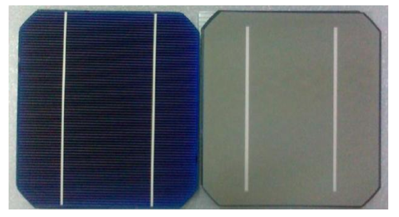 ▲ Front and back of monocrystalline silicon solar cells
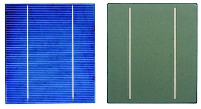 ▲ Front and back of polycrystalline silicon solar cells
Due to the lower purity and curvature requirements for photovoltaic silicon wafers, the manufacturing process is relatively simple. Taking monocrystalline silicon solar cells as an example, the first step is to cut square rods and grind them round; the square rods are cut to size and then the corners are rounded. The second step is acid etching, primarily to remove surface impurities from the monocrystalline square rods. The third step is slicing, where the cleaned square rods are adhered to a workboard. The workboard is then placed on a slicing machine where it is cut according to pre-set process parameters. Finally, the monocrystalline silicon wafers are cleaned and monitored for surface smoothness, resistivity, and other parameters.
Semiconductor silicon wafers: Semiconductor silicon wafers have higher requirements than photovoltaic silicon wafers. First, all silicon wafers used in the semiconductor industry are monocrystalline silicon, in order to ensure that each position of the silicon wafer has the same electrical properties. In terms of shape and size, the monocrystalline silicon wafers for photovoltaic use are square, typically with side lengths of 125mm, 150mm, and 156mm. In contrast, semiconductor monocrystalline silicon wafers are round, with diameters of 150mm (6-inch wafers), 200mm (8-inch wafers), and 300mm (12-inch wafers). In terms of purity, photovoltaic monocrystalline silicon wafers require silicon content between 4N-6N (99.99%-99.9999%), while semiconductor monocrystalline silicon wafers require purity around 9N (99.9999999%)-11N (99.999999999%), which is at least 1000 times higher than that of photovoltaic monocrystalline wafers. In appearance, semiconductor silicon wafers have stricter requirements for surface flatness, smoothness, and cleanliness compared to photovoltaic silicon wafers. Purity is the biggest difference between photovoltaic monocrystalline silicon wafers and semiconductor monocrystalline silicon wafers.
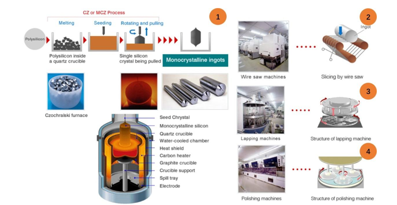 ▲ Semiconductor silicon wafer manufacturing process
The development of Moore’s Law is synonymous with the development of silicon wafers. Since semiconductor silicon wafers are round, they are also known as “silicon wafers” or “wafers.” Wafers are the “substrate” for chip manufacturing; all chips are made on this “substrate.” Throughout the development of semiconductor silicon wafers, there have been two main directions: size and structure.
In terms of size, the trend in silicon wafers is towards larger sizes: In the early days of integrated circuits, 0.75-inch wafers were used. Increasing the wafer area allows for more chips per wafer, reducing costs. Around 1965, with the introduction of Moore’s Law, both integrated circuit technology and silicon wafers entered a period of rapid development. Silicon wafers have passed through milestones of 4-inch, 6-inch, 8-inch, and 12-inch wafers. Since Intel and IBM jointly developed 12-inch wafer chip manufacturing in 2001, the mainstream silicon wafer is now the 12-inch wafer, accounting for about 70%, but 18-inch (450mm) wafers are already on the agenda.
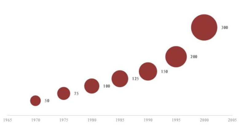 ▲ Parameters of different sized wafers▲ Development of silicon wafer sizes
In terms of structure, the trend in silicon wafers is towards increasing complexity: In the early days of integrated circuits, there was only one type of logic chip, but as application scenarios increased, various types of chips such as logic chips, power devices, analog chips, mixed-signal chips, flash/DRAM memory chips, and RF chips emerged, resulting in different structural forms of silicon wafers. Currently, there are mainly three types:
PW (Polish Wafer): Polished wafers. The silicon wafers obtained by cutting after pulling single crystals are not perfect in terms of smoothness or warpage, so they must first undergo polishing treatment. This method is also the most primitive processing method for silicon wafers.
AW (Anneal Wafer): Annealed wafers. With the continuous development of process technology and the shrinking sizes of transistor features, the drawbacks of polished wafers have gradually become apparent, such as local lattice defects on the wafer surface and a higher oxygen content on the wafer surface. To address these issues, annealed wafer technology was developed. After polishing, the wafers are placed in a furnace filled with inert gas (usually argon) for high-temperature annealing. This can repair lattice defects on the wafer surface and reduce the oxygen content on the surface.
EW (Epitaxy Wafer): Epitaxial wafers. With the increasing application scenarios for integrated circuits, standard silicon wafers produced by silicon wafer manufacturers can no longer meet the electrical characteristics required by certain products. Additionally, the lattice defects reduced by thermal annealing cannot meet the demand for increasingly smaller line widths. This led to the development of epitaxial wafers. The typical epitaxial layer is a silicon thin film, which is grown on the original silicon wafer using thin film deposition technology. In silicon epitaxy, the silicon substrate acts as a seed crystal, so the crystal structure of the epitaxial layer replicates that of the silicon wafer. Since the substrate silicon wafer is monocrystalline, the epitaxial layer is also monocrystalline. However, as it is not polished, the lattice defects on the surface of the grown silicon wafer can be minimized.
The technical indicators for epitaxy mainly include the thickness and uniformity of the epitaxial layer, uniformity of resistivity, control of bulk metal, particle control, and defect control such as layer faults and dislocations. Currently, by optimizing the epitaxy reaction temperature, flow rate of epitaxial gases, and temperature gradients at the center and edges, very high quality of epitaxial silicon wafers has been achieved. Depending on the different products and the need for technological upgrades, high quality epitaxial silicon wafers have now been realized through continuous optimization of epitaxy processes.
In addition, current technology can generate epitaxial layers with different doping elements and doping concentrations from the original silicon wafer, making it easier to control the electrical characteristics of the grown silicon wafers. For example, a layer of N-type silicon epitaxial layer can be generated on a P-type silicon wafer, forming a low concentration doped PN junction, which helps optimize breakdown voltage and reduce latch-up effects in subsequent chip manufacturing. The thickness of the epitaxial layer generally varies depending on the application scenario, with typical logic chip thicknesses ranging from about 0.5 microns to 5 microns, while power devices require thicknesses of around 50 microns to 100 microns.
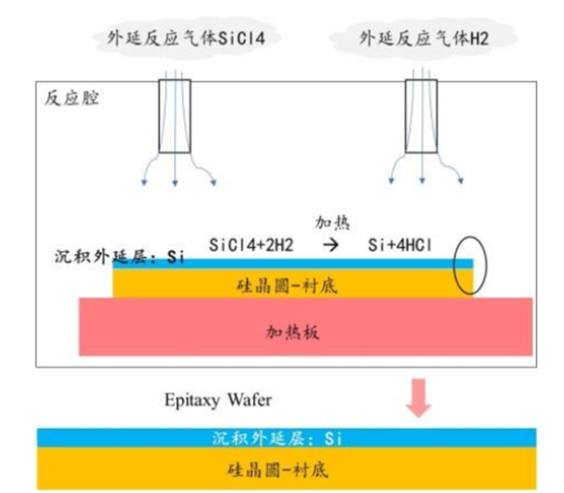 ▲ Epitaxial silicon wafer growth process
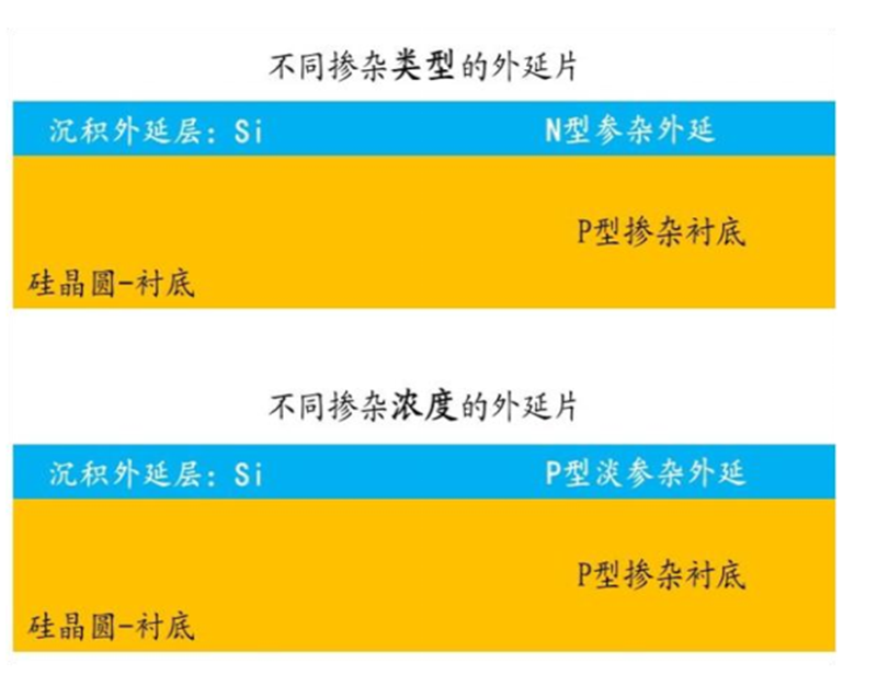 ▲ Different doping of epitaxial wafers
SW (SOI Wafer): SOI stands for Silicon-On-Insulator. Due to the advantages of SOI wafers, such as low parasitic capacitance, small short-channel effects, high integration density, fast speed, and low power consumption, especially the low substrate noise, SOI wafers are often used in RF front-end chips.
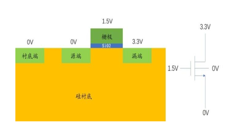 ▲ Regular silicon wafer MOS structure
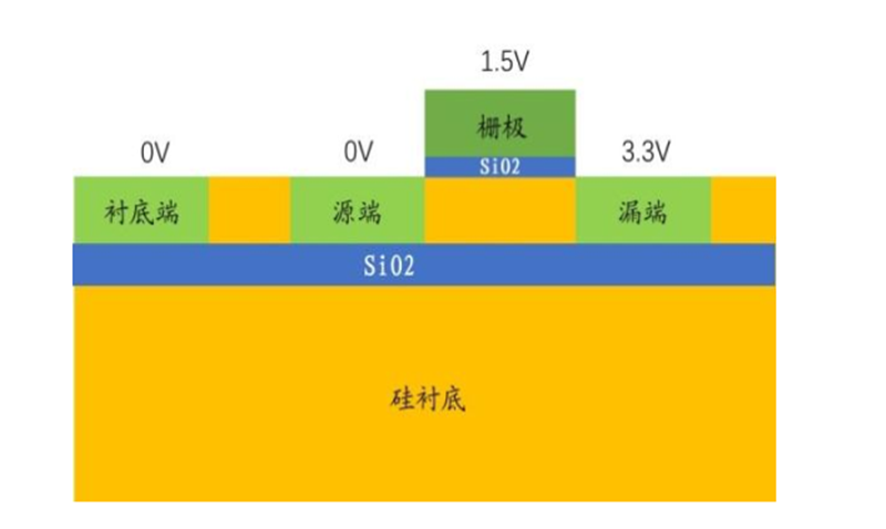 ▲ SOI wafer MOS structure
The methods for manufacturing SOI wafers mainly include four types: SIMOX technology, Bonding technology, Sim-bond technology, and Smart-CutTM technology; the principle of SOI wafers is quite simple, with the core goal being to add an insulating layer (generally silicon dioxide SiO2) in the middle of the substrate.
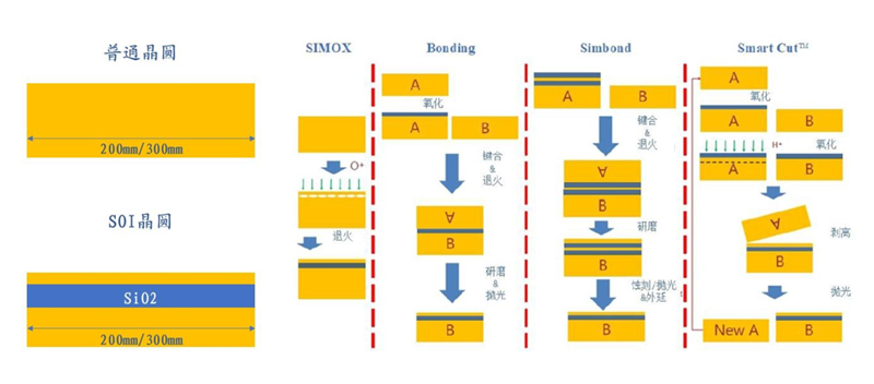 ▲ Four methods for manufacturing SOI wafers
From the perspective of performance parameters, Smart-CutTM technology is currently the most outstanding performance among SOI wafer manufacturing technologies. Sim-bond technology has performance similar to Smart-Cut technology, but in terms of top silicon thickness, SOI wafers produced by Smart-Cut technology are thinner. Additionally, from a production cost standpoint, Smart-Cut technology can reuse silicon wafers, making it more cost-effective for future large-scale production. Thus, the industry widely recognizes Smart-Cut technology as the future direction for SOI wafer development.
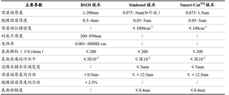 ▲ Performance comparison of different SOI wafer manufacturing technologies
SIMOX technology: SIMOX stands for Separation by Implanted Oxygen. Oxygen atoms are implanted into the wafer, and then high-temperature annealing is performed, causing the oxygen atoms to react with surrounding silicon atoms to form a layer of silicon dioxide. The challenge of this technology is to control the depth and thickness of the oxygen ion implantation, which requires high precision in the ion implantation technology.
Bonding technology: Bonding technology, also known as bonding technology, produces SOI wafers called Bonded SOI, abbreviated as BSOI. This technology requires two ordinary silicon wafers, one of which has a layer of oxide (SiO2) grown on it, which is then bonded to the other silicon wafer. The bonding interface is the oxide layer. Finally, grinding and polishing are performed to achieve the desired depth of the buried layer (SiO2). Since bonding technology is simpler than ion implantation technology, most SOI wafers are currently produced using bonding technology.
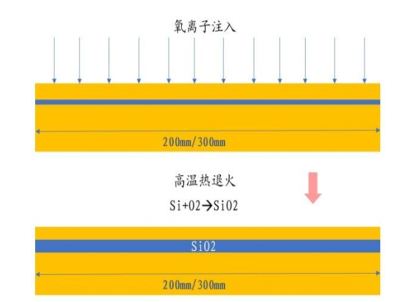 ▲ Ion implantation method for forming silicon on insulator
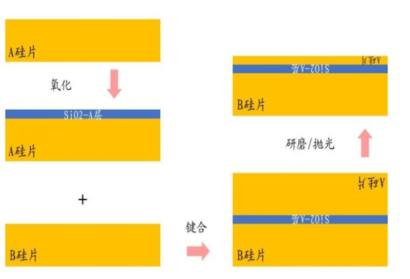 ▲ Wafer bonding method for forming silicon on insulator
Sim-bond technology: Oxygen ion bonding technology. Sim-bond technology is a combination of SIMOX and bonding technology. Its advantage is the high precision control of the buried oxygen layer thickness. The first step is to implant oxygen ions into a silicon wafer, followed by high-temperature thermal annealing to form the oxide layer. The second step is to bond this silicon wafer with another wafer. The third step involves thinning processes using CMP technology, but unlike bonding technology, sim-bond has a self-stop layer that automatically stops when grinding reaches the SiO2 layer. The final step is to etch away the SiO2 layer, followed by polishing.
Smart-cut technology: Smart-cut technology is an extension of bonding technology. The first step is to oxidize a silicon wafer, generating a fixed thickness of SiO2 on the wafer surface. The second step is to use ion implantation technology to inject hydrogen ions to a fixed depth in the wafer. The third step is to bond another wafer to the oxidized wafer. The fourth step is to use low-temperature thermal annealing technology, causing the hydrogen ions to form bubbles, which leads to the separation of part of the silicon wafer. The fifth step is to use high-temperature thermal annealing technology to increase the bonding strength. The final step is to flatten the silicon surface. This technology is recognized internationally as the development direction for SOI technology, with the thickness of the buried oxide layer entirely determined by the depth of hydrogen ion implantation, making it more accurate. Additionally, the separated wafers can be reused, significantly reducing costs.
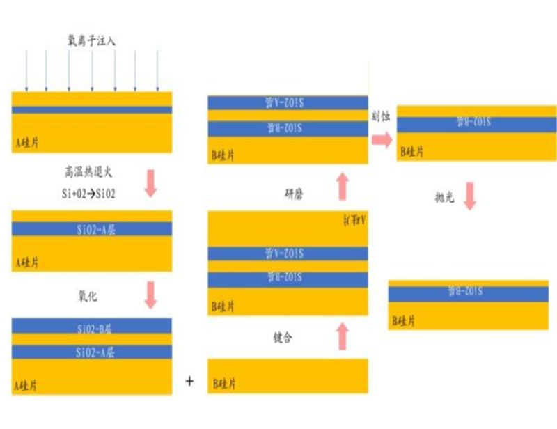 ▲ Sim-bond method for forming silicon on insulator
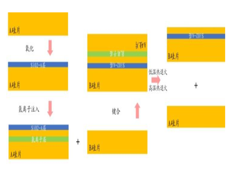 ▲ Smart-cut method for forming silicon on insulator
Source: Smart Things
Disclaimer: This article is sourced from the internet, and the purpose of sharing it is to convey more information. It does not imply agreement with its viewpoints or confirm its authenticity, nor does it constitute other advice. It is merely a platform for communication and does not take responsibility for its copyright. If there are any infringements, please contact us for timely modifications or deletions.