Dear readers, there is an “invisible champion track” hidden in the advanced packaging field of semiconductors—bonding equipment! The explosion of AI computing power, mass production of HBM (High Bandwidth Memory), and the popularization of 3D integration technology have transformed bonding equipment from a “supporting role” in packaging to a “core necessity.” The market scale continues to expand, and domestic manufacturers are making strong breakthroughs. This concise summary clearly breaks down the industry logic, technical trends, and investment opportunities. Save it and keep up with the new wave of the semiconductor industry!
1. Core Logic: End-user Demand + Technological Iteration, Bi-directional Drive for Bonding Equipment Explosion
1.End-user Demand Driving Force: AI servers, electric vehicles, high-end mobile devices, and other scenarios have seen a surge in requirements for chip performance, density, and heat dissipation, forcing upgrades in advanced packaging technology. As bonding is the core process of packaging, the demand for equipment continues to grow;
2.Technological Iteration Driving Force: From traditional wire bonding to flip chip bonding, and then to TCB (Thermal Compression Bonding), hybrid bonding, bonding technology is continuously evolving towards “higher density, smaller pitch, and lower power consumption” with a strong demand for equipment upgrades;
3.Market Size Forecast: The packaging equipment market is expected to grow by 59% from 2024 to 2026, with hybrid bonding equipment having the greatest potential. By 2030, the market space is expected to reach 2.8-3.5 billion euros (approximately 21-26.5 billion RMB).
2. Technical Route: From TCB to Hybrid Bonding, Who Will Be the Future Mainstream?
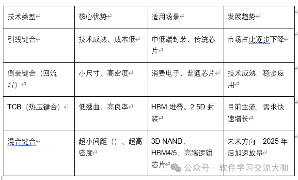
Key Point: Hybrid bonding is the next-generation core technology, eliminating the need for solder bumps and directly achieving copper-to-copper interconnection, meeting the extreme demands of 3D stacking and heterogeneous integration. Samsung, SK Hynix, and TSMC have all laid out their strategies.
3. Core Increment: HBM+CoWoS, Two Major Scenarios Open Up Equipment Space
1.HBM (High Bandwidth Memory):
1. The core necessity for AI computing power, with a demand growth rate of nearly 200% in 2024, and nearly all production capacity sold out by 2025;
2. The stacking process heavily relies on bonding equipment, TCB is currently mainstream, while hybrid bonding will be used for 16 layers and above high-end models;
3. The global market for HBM bonding equipment driven by AI servers is expected to reach 14.31 billion RMB by 2025.
1.CoWoS (Chip on Wafer on Substrate):
1. The mainstream solution for 2.5D packaging, with HBM co-packaged with GPU as the core process;
2. Manufacturers like TSMC and Samsung are accelerating production expansion, driving demand for TCB bonding equipment, with companies like ASMPT already securing large orders.
4. Competitive Landscape: International Giants Dominate, Domestic Substitution Accelerates Breakthroughs
1.International Landscape: The top five global manufacturers hold 86% of the market share, with EV Group (Austria), SUSS (Germany), Besi (Netherlands), and Hanmi Semiconductor (Korea) dominating the high-end market, with mature technology and stable customer resources;
2.Domestic Progress:
1. Breakthroughs in key technologies: companies like Tuojing Technology, Xinhui Lian, and Huazhuo Qingke have launched W2W (Wafer to Wafer), D2W (Die to Wafer) hybrid bonding equipment, with some achieving mass production and repeat orders;
2. Policy + Market Dual Drive: Domestic HBM and advanced packaging capacity are accelerating construction, combined with overseas technology restrictions, domestic equipment is ushering in a “product breakthrough + downstream release” dual opportunity;
3. Key Enterprises: Tuojing Technology (mass production of hybrid bonding equipment), Xinyuan Micro (temporary bonding / debonding machines), Xinhui Lian (first shipment of D2W/W2W equipment), and Quick Intelligent (developing TCB equipment).
5. Investment Highlights: Two Main Lines to Seize Opportunities
1.Technology Leading Type: Focus on hybrid bonding, TCB and other high-end equipment, with manufacturers that have achieved technological breakthroughs and secured customer orders;
2.Domestic Substitution Type: Companies with cost advantages and localized service capabilities in temporary bonding, debonding, surface pre-treatment, and other segments;
Overseas Benchmarking: Hanmi Semiconductor (HBM TCB equipment leader, stock price increased 13 times in two years), Besi (hybrid bonding equipment leader, order growth doubled), providing valuation references for domestic manufacturers.
Dear readers, how long do you think it will take for domestic bonding equipment to break into the high-end market? Which specific technologies are most worth paying attention to? Let’s discuss your views in the comments! You can also leave a message about the companies or technical details you want to learn more about, and we will arrange special analyses for everyone!
#semiconductors #bonding equipment #advanced packaging #HBM #AI chips #domestic substitution #semiconductor equipment #investment strategy