Jiufengshan Laboratory GaN PDK R&D Team
Jiufengshan Laboratory GaN Series Achievements II
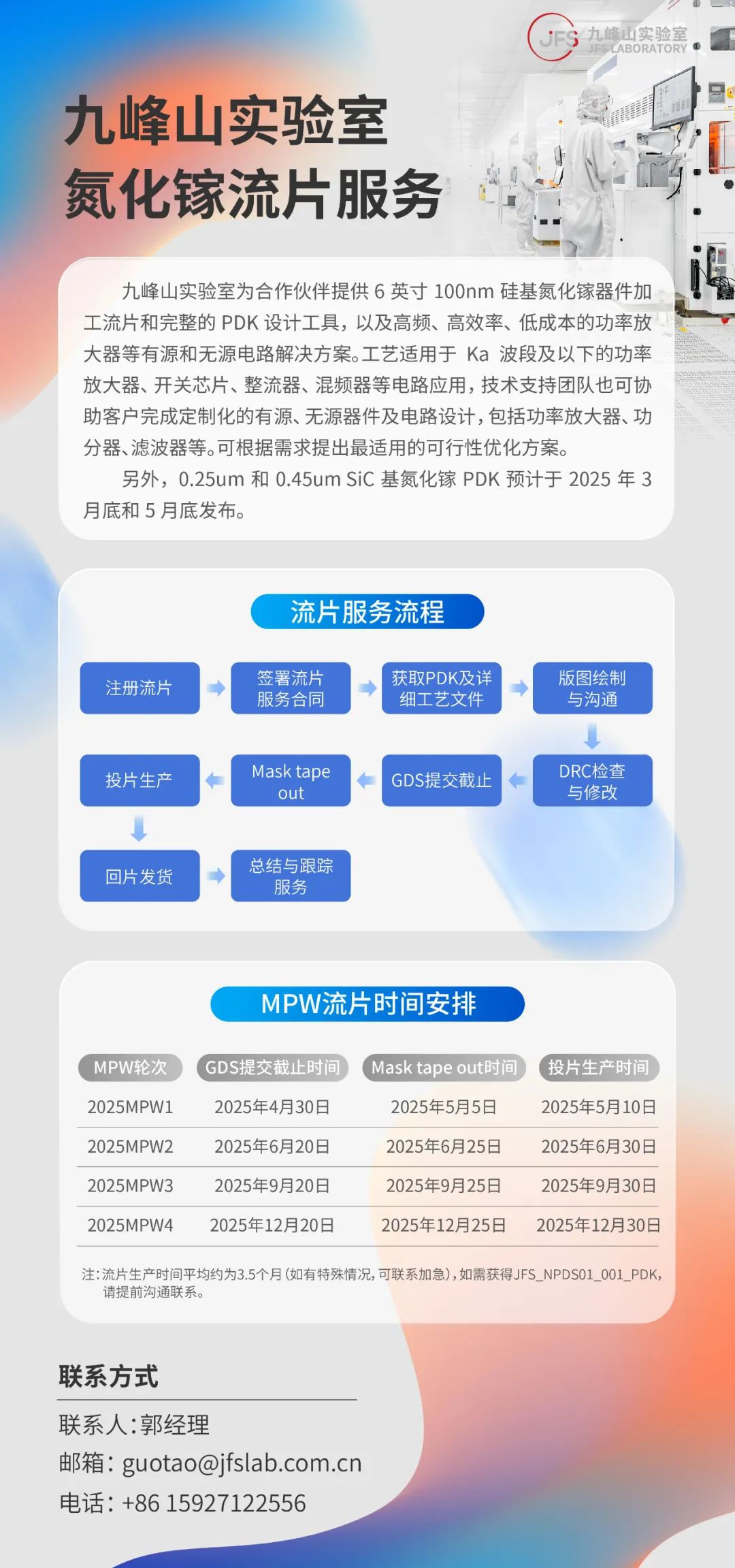
Recently, Jiufengshan Laboratory released the first 100 nm silicon-based GaN commercial Process Design Kit (PDK) in China, with performance indicators reaching domestic leading and international top levels. As the second commercial solution globally and the first in China, its technical specifications support high-throughput Ku/Ka band low Earth orbit satellite communications, meeting the demands for high-frequency, high-power, and high-efficiency GaN devices in next-generation mobile communications, commercial satellite communications, aerospace, vehicle networking, industrial IoT, and mobile terminals, promoting the transition of related device fields in China from “import substitution” to “technology export”.
NEWS
”
PDK (Process Design Kit) is an indispensable toolkit in semiconductor manufacturing. It provides chip designers with critical information such as process parameters, device models, and design rules, facilitating the rapid transformation from circuit design to actual manufacturing, serving as the “bridge” between chip design and manufacturing.
In recent years, with the rapid increase in demand for high-speed, low-latency communication, communication technology is undergoing rapid iteration. Against this backdrop, the market demand for high-performance GaN devices has significantly increased. Among them, silicon-based GaN (GaN-on-Si) technology, with its high efficiency, high power, and high frequency advantages, combined with the benefits of large size and low cost of silicon, has become one of the most promising mainstream solutions in the high-frequency, high-throughput communication field (such as commercial satellite communications) and a technological battleground that countries around the world are competing for.
For silicon-based GaN to achieve breakthroughs in commercial applications, strong PDK design kit support is essential. The PDK released by Jiufengshan Laboratory is the first 100 nm silicon-based GaN commercial Process Design Kit (PDK) in China, having obtained multiple independent intellectual property rights. Its core technological advantages are reflected in:
01
Generational Development
To meet the demands for higher transmission rates and larger bandwidth in scenarios such as high-throughput satellite communications, the technology skips nodes below 150 nm and adopts 100 nm gate length technology, significantly enhancing the cutoff frequency of devices, enabling coverage of DC to Ka band millimeter-wave applications.
02
High Performance
Through epitaxy and device structure design, effectively reducing current collapse, minimizing contact resistance, and improving device efficiency, this series of technological breakthroughs significantly enhances the power consumption and power density of application terminals.
03
Low Cost
Silicon-based GaN technology combines the high-frequency, high-power, and high-efficiency performance advantages of GaN materials with the cost advantages of silicon. In the future, this technology can expand to 8-inch and larger sizes, compatible with CMOS processes, achieving further cost reductions.
#Industry Application Interpretation

(Scene image source: internet)
In the past two years, with the gradual realization of the “direct satellite connection” feature in domestic smartphones, satellite communications have gradually entered the public’s daily life, allowing more people to experience its convenience. The application of silicon-based GaN technology in low Earth orbit commercial satellites perfectly aligns with people’s expectations for high-speed, low-latency communication.
Not only in satellite communications, but GaN devices will also play an increasingly important role in 5G/6G communications, autonomous driving, vehicle networking, IoT, smart cities, and aerospace. A powerful PDK design kit with intellectual property rights lays a solid foundation for the large-scale market application of GaN devices.
For more information on the series of groundbreaking advancements from Jiufengshan Laboratory, please refer to the series of articles published on the same day by this public account.
Note: To better promote the scientific dissemination of compound semiconductor research and development, please contact the backend staff for authorization before reprinting or modifying the original content of this public account.