Source: Semiconductor Full解
Original Author: Yuan Yuan De Yuan
This article introduces the relevant knowledge of power semiconductor IGBT and SiC technology.
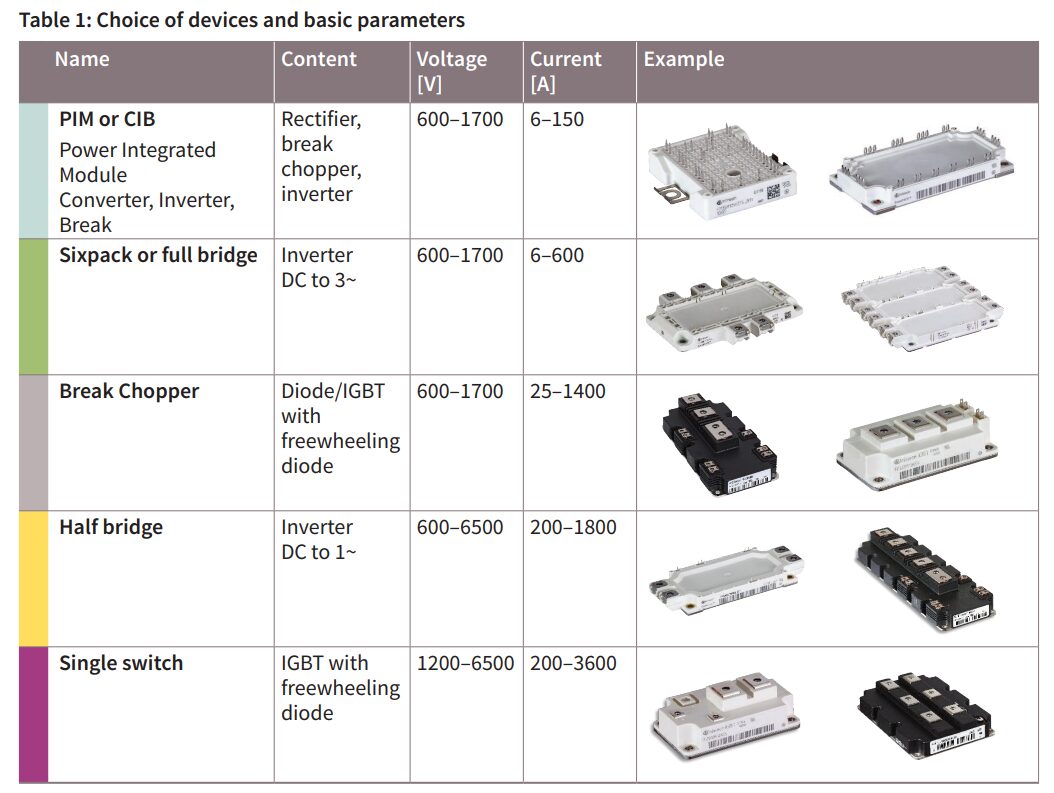
1. Applications of IGBT
Power electronics technology is widely used in new energy vehicles, serving as the basis for efficient, rapid, stable, and safe energy conversion in automotive powertrain systems. The DC/DC topology in new energy vehicles is mainly applied in onboard chargers, the AC/DC topology is mainly used in charging piles, and the DC/AC topology is primarily applied in motor controllers. The motor controller is used to drive the motor after achieving high-power DC/AC conversion and can also capture regenerative braking energy and return it to the battery pack. It is the “heart” of new energy vehicles, determining the vehicle’s functional safety, high-speed stability, and green comfort.
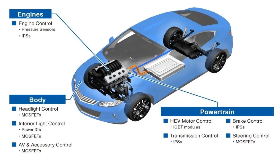
Due to the high demand for range in new energy vehicles, the demand for energy management has become more refined. This has led to a much higher demand for power discrete devices such as Insulated Gate Bipolar Transistors (IGBT), MOSFETs, and diodes compared to traditional vehicles. Power semiconductors account for about 55% of the total vehicle semiconductors in new energy vehicles.
Power semiconductor devices, as the foundation and core of power electronic devices for energy conversion, driving, and control, are one of the key factors driving optimization in terms of conversion efficiency, power density, and size/weight in power electronic systems.
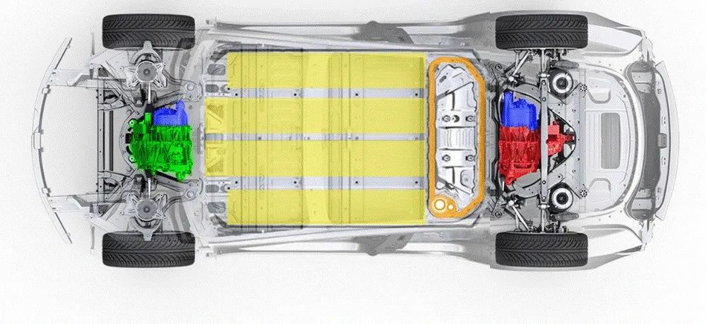
Next, let’s take a look at the distribution of power semiconductor IGBT, where red represents rear-mounted engines and green represents front-mounted engines. Below the cabin floor are four battery packs. The inverter (blue) is integrated within the motor housing and shares the cooling circuit with it. The inverter converts the DC power from the battery to AC power for the motor and is also where the IGBT module is installed.
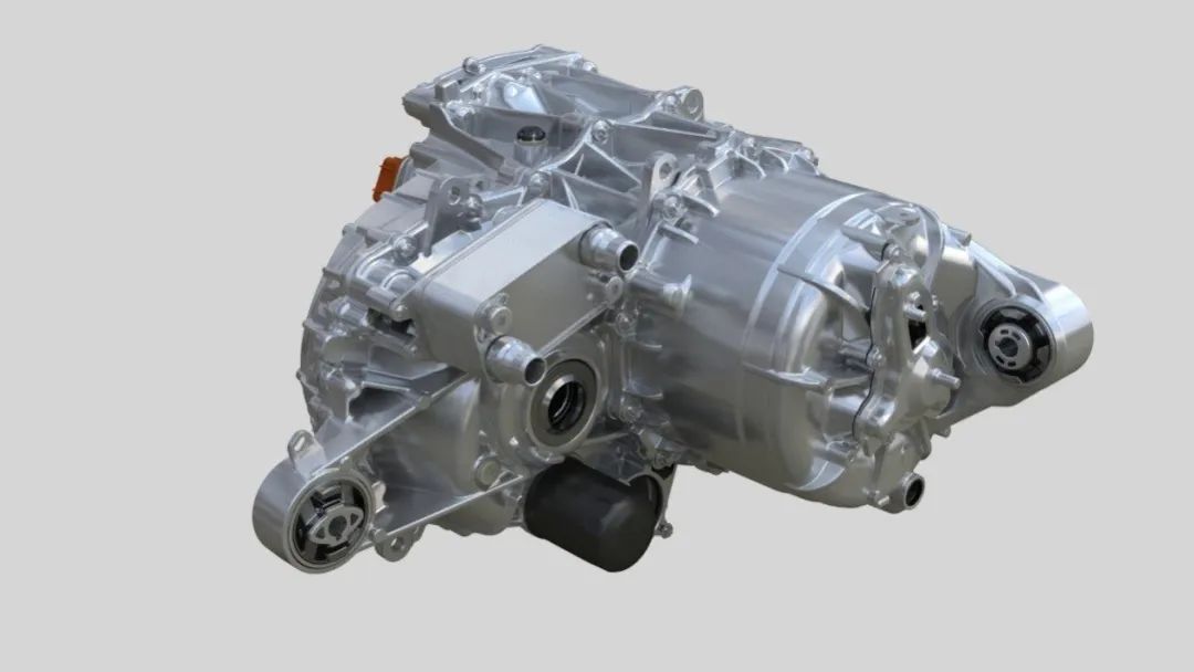
Looking at the power system in isolation, the following diagram shows the power device:
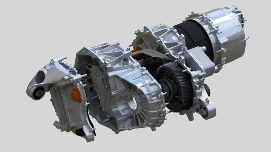
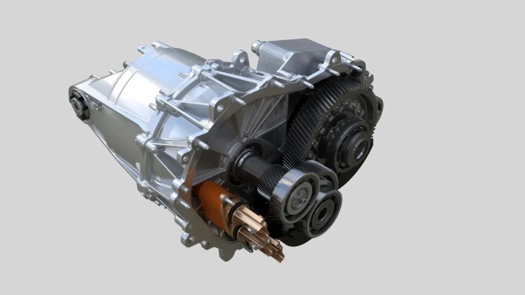
This is an exploded view of the power device, including the motor (stator and rotor), transmission part (gears), and control part (inverter):
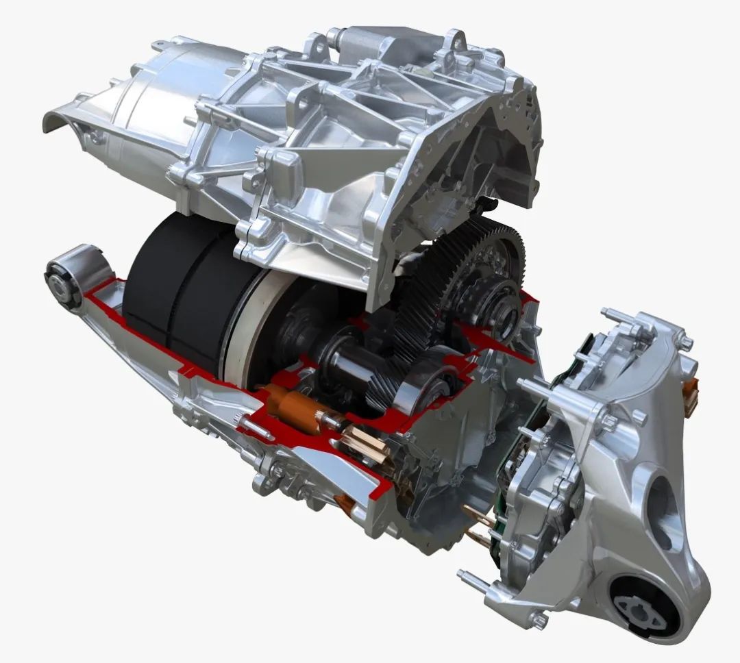
Another view of the power device disassembly:
The following diagram shows a partial detail of the transmission part:
This image is the focus of this article – the inverter! It is also where the power device IGBT is installed:
The next generation of IGBT power devices is shown below:
2. Basic Knowledge of IGBT
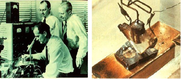
In January 1946, a semiconductor research group was officially established at the BELL laboratory in the United States, consisting of three core members: Schokley, Bardeen, and Brattain, commonly known as the “Transistor Trio”.
The trio had their own research advantages. Bardeen proposed the surface state theory, Schokley provided the basic idea for realizing amplifiers, and Brattain designed the experiments.
The year after the trio was formed, in 1947, Bardeen and Brattain invented the point-contact transistor. Then in 1949, Schokley published a classic paper on p-n junctions and bipolar transistors. In the first transistor in history, two point contacts at the bottom of a triangular quartz crystal were made by pressing gold foil wires spaced 50μm apart onto the semiconductor surface, using germanium as the semiconductor material; when one contact is forward biased (applying positive voltage to the third terminal) and the other contact is reverse biased, transistor action can be observed.
In 1982, RCA and GE jointly developed the composite transistor – Insulated Gate Bipolar Transistor (IGBT). IGBT combines the high input impedance of Metal-Oxide-Semiconductor Field-Effect Transistor (MOSFET) and the high current density of Bipolar Junction Transistor (BJT), providing significant advantages in high-power applications, and was once regarded as an almost ideal power semiconductor device.
Since IGBT integrates the advantages of both BJT and MOSFET, what are BJT and MOSFET?
Before understanding BJT and MOSFET, let’s first understand what a P-N junction is?
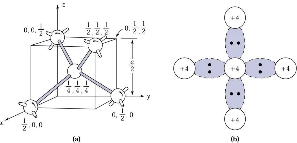
The application of semiconductors is inseparable from silicon. Let’s look at the characteristics of silicon. In the periodic table, silicon is placed in the 14th position, and silicon atoms have 4 electrons in the outer layer, which share 4 pairs of electrons with 4 surrounding atoms. This structure of shared electron pairs is called covalent bonding. Each electron pair forms a covalent bond. This part of knowledge is learned in middle school chemistry. Let’s look at a picture for a visual understanding:
The left image shows the crystal structure of single crystal silicon, which has a diamond crystal structure. The right image shows the situation of silicon atoms sharing electrons, with one silicon atom sharing electrons with four silicon brothers.
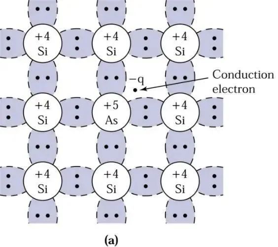
One day, a physicist thought about a question: What if silicon does not share electrons with silicon brothers but brings other brothers into the group? One day, the physicist brought arsenic brother into the group, and a miracle happened:
The arsenic brother has 5 electrons in the outer layer, four of which found partners in the silicon family, while one electron remained single. This electron became a vagrant, wandering around. Since electrons carry charge, it changed the conductivity of the silicon family. At this point, the arsenic atom provided an extra electron to the silicon family, hence it is called a donor.
With the increase of free electrons, the negatively charged carriers increase, and silicon becomes n-type semiconductor. Why is it called n-type? In English, “Negative” represents negative, and the first letter of that word is N.
Similarly, physicists thought, since they can bring in arsenic which has more electrons, can they also bring in boron atoms which have fewer electrons? So the physicist tried bringing in boron atoms.
Since boron atoms have only 3 electrons in the outer layer, one less than silicon, the originally paired covalent bonds now have one less pair of electrons, resulting in a vacant position, forming a positively charged hole. At this point, the silicon-based semiconductor is called a p-type semiconductor, and similarly, P comes from the first letter of the English word “Positive”, while boron atoms are called acceptors.
The junction formed by the contact of p-type and n-type semiconductors is called a PN junction.
For example, the p-type semiconductor is like a square piece of clay with many holes (holes), similar to lobster holes we see. The n-type semiconductor is also a square piece of clay, but it has many lobsters (free electrons) hidden inside. When we stick these two pieces of clay together, the lobsters will crawl towards the lobster holes (electron drift). Under the drift of electrons, current is formed in the PN junction.
Now let’s talk about the function of transistors. A transistor (transistor is an abbreviation for transfer resistor) is a multi-junction semiconductor device. Transistors are usually integrated with other circuit devices to gain voltage, current, or signal power gain.
In circuits, the main function of a transistor is to act as a switch. A small base current can be used to change the collector current from off to on (and vice versa) in a very short time. Off means high voltage and low current, while on means low voltage and high current.
How to understand bipolar transistors? Bipolar transistors are semiconductor devices in which both electrons and holes participate in conduction, composed of two adjacent coupled p-n junctions, which can be in the form of p-n-p or n-p-n.
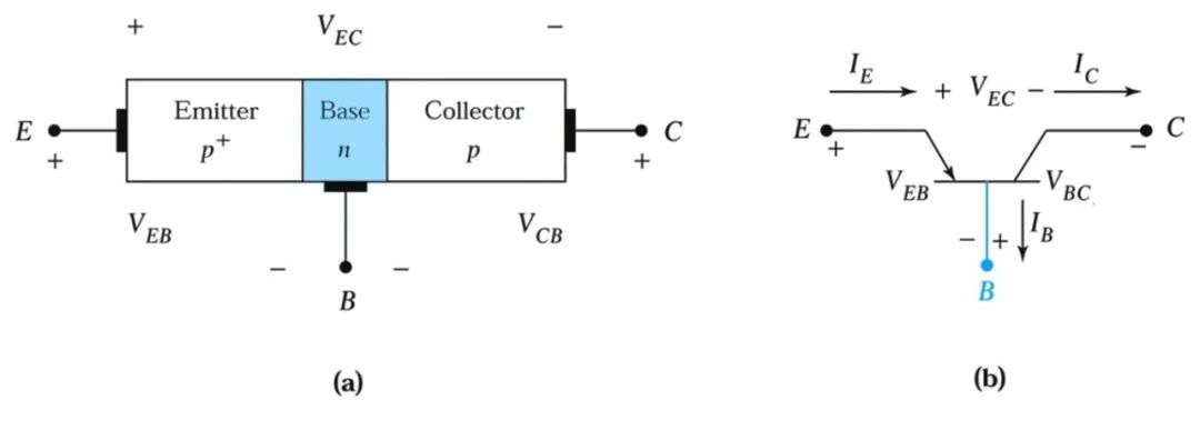
The following diagram shows a perspective view of a p-n-p bipolar transistor. Its manufacturing process involves using p-type semiconductor as the substrate, forming an n-type region on the p-type substrate using thermal diffusion, and then forming a high concentration p+ region on this n-type region, followed by metal covering the p+, n, and underlying p-type regions to form ohmic contacts.
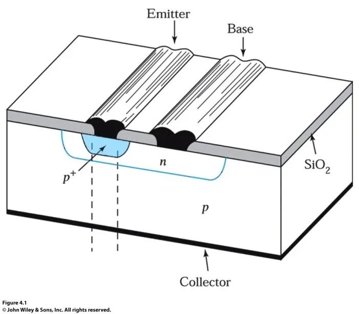 The following diagram shows a p-n-p bipolar transistor, which has three regions with different doping concentrations, forming two p-n junctions. The highest concentration p+ region is called the emitter (represented by E); the narrower n-type region with moderate impurity concentration is called the base (represented by B), and the width of the base must be much smaller than the diffusion length of minority carriers; the lowest concentration p-type region is called the collector (represented by C). Assuming the concentrations in each region are uniformly distributed, the concept of p-n junction can be directly applied to the junctions within the transistor.
After understanding BJT, let’s look at the definition of MOSFET. First, let’s understand the first half of MOSFET, which is the MOS device.
Metal-Oxide-Semiconductor (MOS) capacitors play an important role in semiconductor devices and are one of the most useful devices for studying semiconductor surface properties. They are also the hub of the most important MOSFET devices in advanced integrated circuits.
The ideal MOS capacitor has the following cross-sectional structure, where d is the thickness of the oxide layer, and V is the voltage applied to the metal plate. When the metal plate is positively biased relative to the ohmic contact, V is positive; when the metal plate is negatively biased relative to the ohmic contact, V is negative.
MOSFET has several abbreviations, such as IGFET (Insulated-Gate Field-Effect Transistor), MISFET (Metal-Insulating-Semiconductor Field-Effect Transistor), and MOST (Metal-Oxide-Semiconductor Transistor).
The n-channel MOSFET is a four-terminal device composed of a p-type semiconductor with two n+ regions (source and drain). For the p-channel MOSFET, the doping types of the substrate and source/drain regions are n and p+, respectively.
The metal on the oxide layer is called the gate. Highly doped or metal silicide such as WSi2 can be used as the gate electrode, and the fourth terminal is the ohmic contact connected to the substrate.
The basic device parameters include channel length L (the distance between the two n+-p junctions), channel width Z, oxide layer thickness d, junction depth rj, and substrate doping concentration NA. The center of the device is the MOS capacitor.
The basic characteristics of MOSFET: The source terminal serves as a voltage reference point. When there is no external bias voltage at the gate, the source-drain electrodes can be considered as two back-to-back p-n junctions, and the current flowing from the source to the drain is only the reverse leakage current.
These definitions may sound complicated, but their overall function is similar to a faucet switch, which can control the direction and size of water flow. The internal structure differences between MOSFET, BJT, and IGBT can be seen in the following diagram:
3. Internal Structure of IGBT
Having said so much, how is the IGBT module manufactured? What are the technical difficulties?
The following image shows several typical IGBT modules:
Disassembling one of the IGBT modules, the internal structure of the IGBT module is shown in the following diagram. During the manufacturing process, it can be mainly divided into two parts: one part is the packaging and testing of the IGBT chip, and the other part is the design and manufacturing of the IGBT chip:
If we further categorize the structure of the IGBT module, it can be divided into the following parts:
The IGBT module mainly includes the following interconnection structure layers:
(1) Chip: includes IGBT chip and diode chip, which are the core structures of the IGBT module.
(2) Direct Copper Bonded (DCB) ceramic substrate: consists of an upper copper layer, a ceramic substrate layer, and a lower copper layer. The upper copper layer is etched into a circuit as needed, providing interconnection for the IGBT chip’s collector, emitter, and gate electrodes. The ceramic substrate layer is usually made of aluminum oxide or aluminum nitride, providing insulation for the chip and its underlying structure while supporting and dissipating heat from the chip. The lower copper layer primarily provides a heat dissipation path for various chips.
(3) Copper substrate: provides a heat dissipation channel for the chip and supports the upper structure layer.
(4) Solder layer: mainly connects the chip, the upper copper layer of the direct copper bonded ceramic substrate, the lower copper layer of the direct copper bonded ceramic substrate, and the copper substrate.
(5) Al bonding wire: usually uses multiple parallel wires, with one end bonded to the chip and the other end bonded to the upper copper layer of the direct copper bonded ceramic substrate. The main function of the Al bonding wire is to achieve interconnection between the chip and external terminal connections.
(6) Al metallization layer: has good ductility and conductivity, facilitating the bonding of the IGBT chip to the Al lead wire.
(7) External connection terminals: include the emitter busbar and collector busbar, which connect to the upper copper layer of the direct copper bonded ceramic substrate at one end and are exposed to the external device at the other end, mainly achieving interconnection between the IGBT chip and external circuits.
(8) Silicone: protects the interconnection structure layers from external acid and alkali corrosion, and also protects the interconnection structure layers from vibration and shock.
(9) Housing: includes side frames and top covers made of epoxy resin, protecting the internal interconnection structure layers of the IGBT module from external environmental influences.
4. IGBT Module Packaging Technology
Before explaining the manufacturing stage of the IGBT module, let’s first understand the packaging part of the IGBT module.
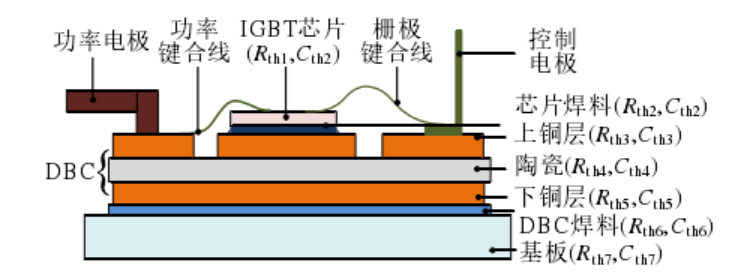
The appearance and cross-section of a typical power module are shown in the following images, where the upper copper layer arranges the power semiconductor/diode chips/bonding wires, etc., and the DBC provides circuit layout, insulation, heat transfer, and mechanical support functions. The heat dissipation substrate supports the backing plate from above and contacts the heat transfer medium from below. The main components in the heat transfer path are the power chip, chip solder, upper copper layer, ceramic, lower copper layer, DBC solder, and substrate.
The following diagram shows a p-n-p bipolar transistor, which has three regions with different doping concentrations, forming two p-n junctions. The highest concentration p+ region is called the emitter (represented by E); the narrower n-type region with moderate impurity concentration is called the base (represented by B), and the width of the base must be much smaller than the diffusion length of minority carriers; the lowest concentration p-type region is called the collector (represented by C). Assuming the concentrations in each region are uniformly distributed, the concept of p-n junction can be directly applied to the junctions within the transistor.
After understanding BJT, let’s look at the definition of MOSFET. First, let’s understand the first half of MOSFET, which is the MOS device.
Metal-Oxide-Semiconductor (MOS) capacitors play an important role in semiconductor devices and are one of the most useful devices for studying semiconductor surface properties. They are also the hub of the most important MOSFET devices in advanced integrated circuits.
The ideal MOS capacitor has the following cross-sectional structure, where d is the thickness of the oxide layer, and V is the voltage applied to the metal plate. When the metal plate is positively biased relative to the ohmic contact, V is positive; when the metal plate is negatively biased relative to the ohmic contact, V is negative.
MOSFET has several abbreviations, such as IGFET (Insulated-Gate Field-Effect Transistor), MISFET (Metal-Insulating-Semiconductor Field-Effect Transistor), and MOST (Metal-Oxide-Semiconductor Transistor).
The n-channel MOSFET is a four-terminal device composed of a p-type semiconductor with two n+ regions (source and drain). For the p-channel MOSFET, the doping types of the substrate and source/drain regions are n and p+, respectively.
The metal on the oxide layer is called the gate. Highly doped or metal silicide such as WSi2 can be used as the gate electrode, and the fourth terminal is the ohmic contact connected to the substrate.
The basic device parameters include channel length L (the distance between the two n+-p junctions), channel width Z, oxide layer thickness d, junction depth rj, and substrate doping concentration NA. The center of the device is the MOS capacitor.
The basic characteristics of MOSFET: The source terminal serves as a voltage reference point. When there is no external bias voltage at the gate, the source-drain electrodes can be considered as two back-to-back p-n junctions, and the current flowing from the source to the drain is only the reverse leakage current.
These definitions may sound complicated, but their overall function is similar to a faucet switch, which can control the direction and size of water flow. The internal structure differences between MOSFET, BJT, and IGBT can be seen in the following diagram:
3. Internal Structure of IGBT
Having said so much, how is the IGBT module manufactured? What are the technical difficulties?
The following image shows several typical IGBT modules:
Disassembling one of the IGBT modules, the internal structure of the IGBT module is shown in the following diagram. During the manufacturing process, it can be mainly divided into two parts: one part is the packaging and testing of the IGBT chip, and the other part is the design and manufacturing of the IGBT chip:
If we further categorize the structure of the IGBT module, it can be divided into the following parts:
The IGBT module mainly includes the following interconnection structure layers:
(1) Chip: includes IGBT chip and diode chip, which are the core structures of the IGBT module.
(2) Direct Copper Bonded (DCB) ceramic substrate: consists of an upper copper layer, a ceramic substrate layer, and a lower copper layer. The upper copper layer is etched into a circuit as needed, providing interconnection for the IGBT chip’s collector, emitter, and gate electrodes. The ceramic substrate layer is usually made of aluminum oxide or aluminum nitride, providing insulation for the chip and its underlying structure while supporting and dissipating heat from the chip. The lower copper layer primarily provides a heat dissipation path for various chips.
(3) Copper substrate: provides a heat dissipation channel for the chip and supports the upper structure layer.
(4) Solder layer: mainly connects the chip, the upper copper layer of the direct copper bonded ceramic substrate, the lower copper layer of the direct copper bonded ceramic substrate, and the copper substrate.
(5) Al bonding wire: usually uses multiple parallel wires, with one end bonded to the chip and the other end bonded to the upper copper layer of the direct copper bonded ceramic substrate. The main function of the Al bonding wire is to achieve interconnection between the chip and external terminal connections.
(6) Al metallization layer: has good ductility and conductivity, facilitating the bonding of the IGBT chip to the Al lead wire.
(7) External connection terminals: include the emitter busbar and collector busbar, which connect to the upper copper layer of the direct copper bonded ceramic substrate at one end and are exposed to the external device at the other end, mainly achieving interconnection between the IGBT chip and external circuits.
(8) Silicone: protects the interconnection structure layers from external acid and alkali corrosion, and also protects the interconnection structure layers from vibration and shock.
(9) Housing: includes side frames and top covers made of epoxy resin, protecting the internal interconnection structure layers of the IGBT module from external environmental influences.
4. IGBT Module Packaging Technology
Before explaining the manufacturing stage of the IGBT module, let’s first understand the packaging part of the IGBT module.
The appearance and cross-section of a typical power module are shown in the following images, where the upper copper layer arranges the power semiconductor/diode chips/bonding wires, etc., and the DBC provides circuit layout, insulation, heat transfer, and mechanical support functions. The heat dissipation substrate supports the backing plate from above and contacts the heat transfer medium from below. The main components in the heat transfer path are the power chip, chip solder, upper copper layer, ceramic, lower copper layer, DBC solder, and substrate.
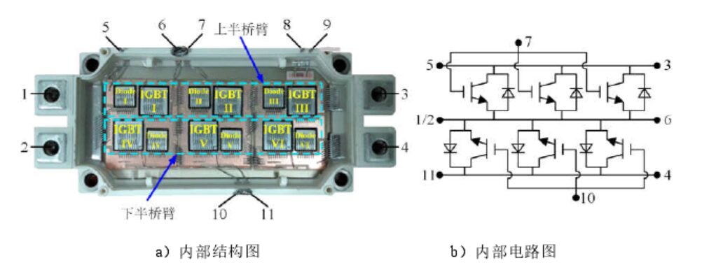
 The following image shows the internal structure of an IGBT module, integrating 6 IGBT chips named IGBT I, II, III, IV, V, and VI. These 6 IGBT chips are connected in parallel to form the upper half-bridge arm, while IGBT IV, V, and VI are connected in parallel to form the lower half-bridge arm, with the two half-bridge arms connected in series. Each IGBT chip has a diode connected in reverse parallel at both ends to achieve current continuity.
In addressing the packaging issues of IGBT, most efforts have focused on solving the heat dissipation of IGBT modules, as any power device is more prone to aging and failure in high-temperature environments.
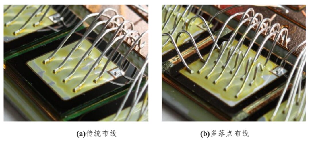
In optimizing the packaging structure of the IGBT, two aspects have been considered: one is the bonding method of the lead wires during the packaging process, commonly referred to as bonding, and the other is the optimization of the chip layout.
In optimizing the bonding method, increasing the number of bonding points helps to reduce the current density around the bonding points in the chip’s metal layer. After adding a bonding point, the maximum current density in the chip’s metal layer decreased by 20%, which improved the power cycling performance by 4 times. Since then, multi-bonding wire structures have been widely adopted in high-current large-area chips.
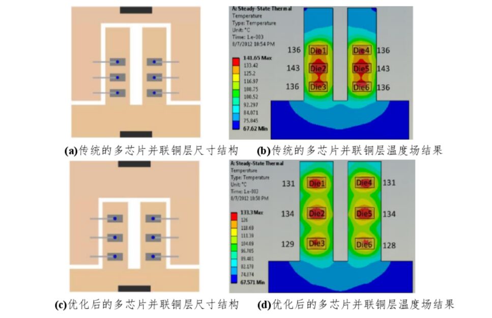
To effectively alleviate the thermal stress of bonding points, diverse bonding wire layout methods can be used to reduce chip temperature. ABB proposed a multi-bonding wire structure, which is compared to traditional wiring in the diagram below.
Thermodynamic simulation analysis of different chip layout methods shows that the heat dissipation varies under different layouts:
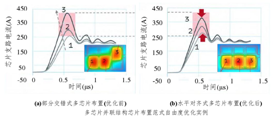
Therefore, scholars at home and abroad have conducted preliminary practices on thermal optimization of the packaging layout of electric control power modules. By adjusting the positions of chips in parallel multi-chip structures to be closer to the emitter electrode, the layout of chips was changed from partially staggered to horizontally aligned, reducing the current imbalance from 50% to 33%.
Depending on the design of different products, the layout design freedom includes the number of loops, chip layout paradigms, DBC size, bonding wiring paradigms, bonding DBC bonding point locations, Kelvin wiring, and emitter electrode positions.
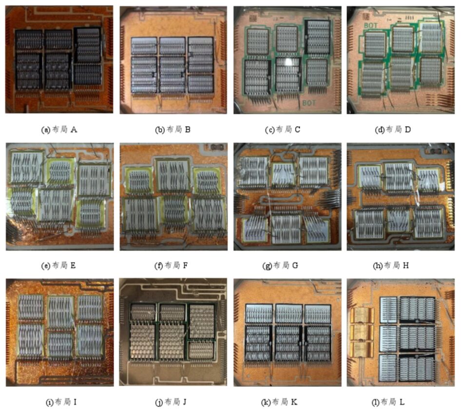
The following image shows the chip layout methods of different companies’ IGBT modules:
By summarizing the packaging layout characteristics of each module, it can be concluded that the bonding wire can be arranged in parallel, staggered, or layered, while multi-chip layouts can be partially staggered, continuously staggered, horizontally aligned, or vertically aligned.
Among them, images (g) and (h) adopt a multi-chip layout with a double-loop structure. Image (d) uses a series Kelvin wiring structure between multi-chips. In image (g), the emitter electrode is placed below chip 1.
By optimizing the layout of the IGBT chips, the branch current can be effectively reduced, lowering the heat generation of a single chip. The following image shows the changes in chip branch current after optimizing the layout of three chips.
5. IGBT Chip Manufacturing Technology
The production process of power device IGBT module chips is long, complex, and detailed, but the process flow is summarized in the following diagram:
The IGBT substrate is a P-N junction
Using ion implantation equipment to perform ion injection on the P-N junction
The following image shows the internal structure of an IGBT module, integrating 6 IGBT chips named IGBT I, II, III, IV, V, and VI. These 6 IGBT chips are connected in parallel to form the upper half-bridge arm, while IGBT IV, V, and VI are connected in parallel to form the lower half-bridge arm, with the two half-bridge arms connected in series. Each IGBT chip has a diode connected in reverse parallel at both ends to achieve current continuity.
In addressing the packaging issues of IGBT, most efforts have focused on solving the heat dissipation of IGBT modules, as any power device is more prone to aging and failure in high-temperature environments.
In optimizing the packaging structure of the IGBT, two aspects have been considered: one is the bonding method of the lead wires during the packaging process, commonly referred to as bonding, and the other is the optimization of the chip layout.
In optimizing the bonding method, increasing the number of bonding points helps to reduce the current density around the bonding points in the chip’s metal layer. After adding a bonding point, the maximum current density in the chip’s metal layer decreased by 20%, which improved the power cycling performance by 4 times. Since then, multi-bonding wire structures have been widely adopted in high-current large-area chips.
To effectively alleviate the thermal stress of bonding points, diverse bonding wire layout methods can be used to reduce chip temperature. ABB proposed a multi-bonding wire structure, which is compared to traditional wiring in the diagram below.
Thermodynamic simulation analysis of different chip layout methods shows that the heat dissipation varies under different layouts:
Therefore, scholars at home and abroad have conducted preliminary practices on thermal optimization of the packaging layout of electric control power modules. By adjusting the positions of chips in parallel multi-chip structures to be closer to the emitter electrode, the layout of chips was changed from partially staggered to horizontally aligned, reducing the current imbalance from 50% to 33%.
Depending on the design of different products, the layout design freedom includes the number of loops, chip layout paradigms, DBC size, bonding wiring paradigms, bonding DBC bonding point locations, Kelvin wiring, and emitter electrode positions.
The following image shows the chip layout methods of different companies’ IGBT modules:
By summarizing the packaging layout characteristics of each module, it can be concluded that the bonding wire can be arranged in parallel, staggered, or layered, while multi-chip layouts can be partially staggered, continuously staggered, horizontally aligned, or vertically aligned.
Among them, images (g) and (h) adopt a multi-chip layout with a double-loop structure. Image (d) uses a series Kelvin wiring structure between multi-chips. In image (g), the emitter electrode is placed below chip 1.
By optimizing the layout of the IGBT chips, the branch current can be effectively reduced, lowering the heat generation of a single chip. The following image shows the changes in chip branch current after optimizing the layout of three chips.
5. IGBT Chip Manufacturing Technology
The production process of power device IGBT module chips is long, complex, and detailed, but the process flow is summarized in the following diagram:
The IGBT substrate is a P-N junction
Using ion implantation equipment to perform ion injection on the P-N junction
3. Formation of Insulation Film
Forming a mask insulation layer through CVD
4. Processing of Mask Insulation Film
Processing the insulation film through etching and stripping
5. P+ Injection
Using ion implantation equipment for P ion injection
6. Formation of Grooves
Forming grooves through etching
7. Formation of Insulation Film
Forming an insulation film again through CVD
8. Processing of Insulation Film
Processing the insulation film through etching and stripping
9. Formation of Emitter Electrode
Forming the electrode through sputtering or evaporation
10. Formation of P+FS Layer
Forming the P+FS layer through ion implantation equipment
11. Formation of B+(Collector)
Forming B+(Collector) through ion implantation equipment
12. Formation of Collector
Forming the Collector through sputtering or evaporation
Through the above processes, a standard IGBT chip manufacturing process is completed.
The following image shows the detailed internal structure of the IGBT chip:
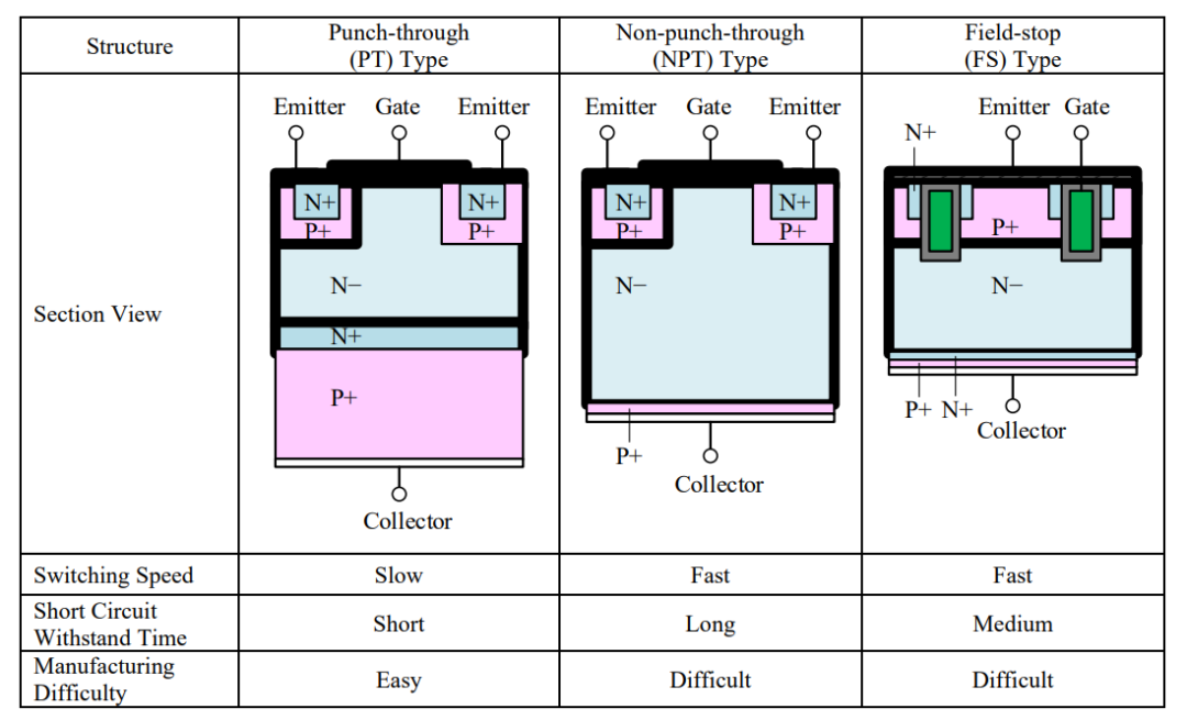
Depending on the design differences of the internal structure of the IGBT chip, it can be divided into PT type, NPT type, and FS type, as shown in the following image:
6. Advantages and Applications of SiC IGBT
The highest reported breakdown voltage of Si IGBT is 8.4kV, which is very close to the limit of Si devices. Additionally, operating frequency and junction temperature are also major limiting factors for Si IGBT.
Silicon Carbide (SiC) Insulated Gate Bipolar Transistor (IGBT) has broad application potential in ultra-high voltage applications such as ultra-high voltage power transmission systems.
The following image shows a Silicon Carbide (SiC) IGBT module:
SiC was discovered in 1823 in the chemistry laboratory of Karolinska University in Stockholm by Professor Jons Berzelius. In 1987, CREE reported the manufacture of 6H-SiC single crystal, marking the formal entry of SiC into a rapidly developing era, with CREE becoming the world’s first company to manufacture and sell SiC wafers and devices.
In 2001, the first commercial SiC diode device was launched, and SiC switching devices gradually matured. The development of Junction Field Effect Transistor (JFET) and Metal-Oxide-Semiconductor Field Effect Transistor (MOSFET) gradually transitioned from laboratory research to commercialization. JFET and MOSFET devices are unipolar devices with high switching speeds, mainly suitable for the range of 0.6kV to 10kV, while Bipolar Junction Transistor (BJT), Insulated Gate Bipolar Transistor (IGBT), and Gate Turn-off Thyristor (GTO) are bipolar devices suitable for high voltage ranges above 10kV.
In 2006, the world’s first commercial SiC switching device JFET was released. In 2008, the first SiC BJT device and normally-off SiC JFET were released. However, the productization of MOSFET devices remained blank. With the development of process technology, especially the maturity of gate oxide interface treatment technology, in 2010, Cree and Rohm launched planar gate MOSFET products.
In 2015, Rohm switched from the original planar gate MOSFET technology route to the trench gate MOSFET, and Infineon released trench gate MOSFET products in 2017.
The following table lists the material properties of several common semiconductors, from which it can be seen that the bandgap of 4H-SiC is about three times that of Si, and at the same temperature, SiC has a lower intrinsic carrier concentration; the critical electric field is about ten times higher, allowing SiC to withstand higher voltages; the saturation drift velocity is about twice as high, giving SiC devices high-speed and high-frequency characteristics; and the thermal conductivity is about three times higher, enabling SiC devices to operate at higher temperatures, thereby reducing the size of the cooling system and the overall system volume.
 At the same time, although SiC is a compound semiconductor material, it can still form a silicon dioxide (SiO2) layer on it through thermal oxidation, which is very beneficial for the manufacture of SiC gate-controlled devices. All these advantages make SiC, along with Gallium Nitride (GaN) and diamond materials, known as third-generation semiconductor materials with broad development prospects.
Thanks to the excellent material properties of SiC, SiC IGBT has an irreplaceable position in ultra-high voltage (≥15kV) applications, such as power transmission, power storage, ultra-high voltage grid interfaces, and electric management systems in all-electric propulsion systems for ships and all-electric propulsion spacecraft.
Currently, SiC IGBT has become a key focus of semiconductor research in various countries.
7. Internal Structure of SiC IGBT
Silicon Carbide MOSFET is currently the most concerned switching device among SiC devices, with major power device companies (Cree, ST, Rohm, Infineon, etc.) launching related products. Each generation of products has made continuous progress in cell design, conduction voltage drop, and gate drive voltage. Among them, Cree and ST focus on the development of planar gate MOSFETs, while Rohm launched the third generation trench gate MOSFET after introducing the first and second generations of planar gate MOSFETs.
The trend in the development of MOSFET devices is to achieve smaller specific conduction resistance.
With the gradual maturity of material growth and processing, SiC is gradually applied to vertical power devices. However, due to the limitations of SiC ion implantation process levels in the early stages, researchers adopted epitaxial doping methods to grow the N+ region and P-well region of MOSFET. Due to the simplicity of the trench MOSFET process, this process became the first to be used for developing SiC MOSFET devices in 1993.
Due to the low breakdown voltage of trench MOSFETs, and with the continuous maturity of ion implantation and high-temperature annealing activation processes, the research focus shifted from trench MOSFETs to planar gate double-injection MOSFET (DMOSFET).
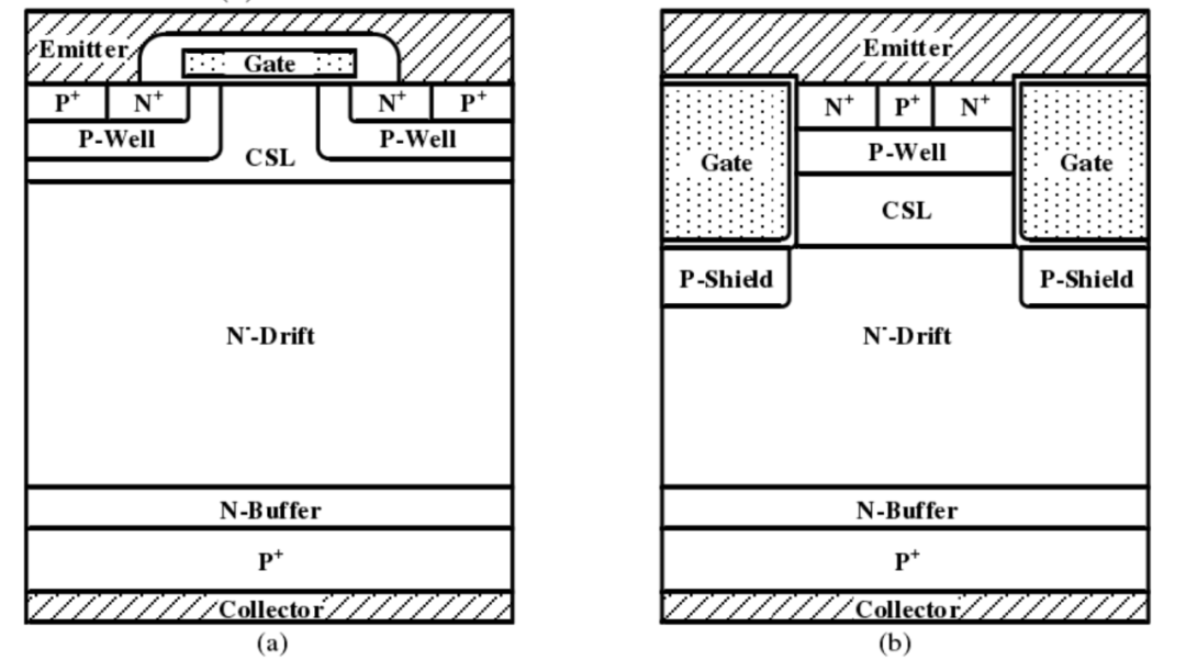
The cell structure of traditional N-channel SiC IGBT devices is shown in the following diagram, where (a) is the planar structure, and (b) is the trench structure.
During chip manufacturing, N-type ion implantation processes in silicon carbide materials commonly use nitrogen ions (N) and phosphorus ions (P) as doping ions. For P-type ion implantation in silicon carbide materials, common doping ions include aluminum ions (Al) and boron ions (B).
After the ion implantation process, a large number of defects are generated in the implanted area, and most of the doping ions remain in the interstitial positions, failing to achieve effective activation, thus requiring annealing processes to repair the defects.
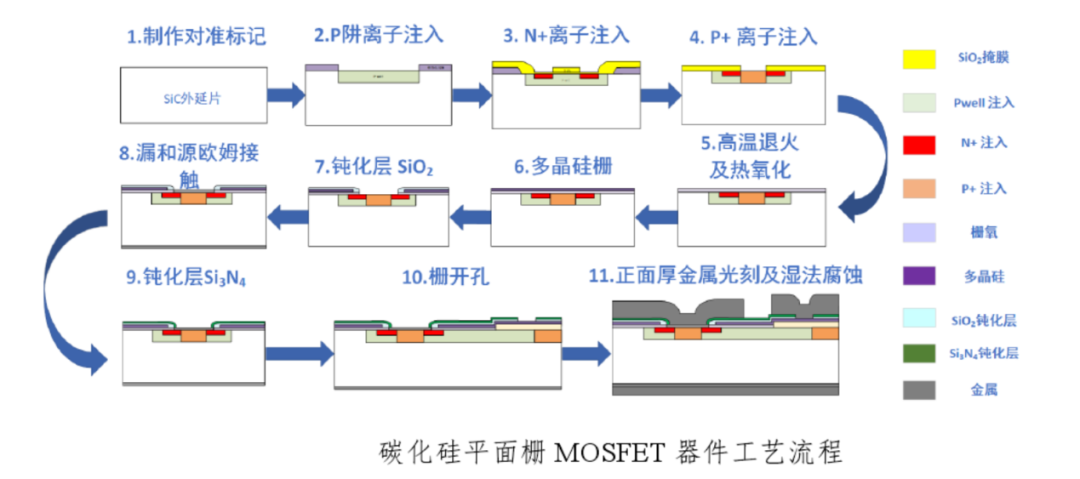
The process of silicon carbide planar gate MOSFET devices is shown in the following diagram.
The first step requires making alignment marks on the epitaxial wafer, which need to be aligned with the subsequent patterns. The second to fourth steps all require ion implantation processes. The ion implantation process determines the morphology and interrelationship of the junctions, which is especially important in planar gate MOSFETs.
The second step uses aluminum for P-well ion implantation.
The third step uses nitrogen for N+ ion implantation.
The fourth step uses aluminum for simultaneous ion implantation of the source region and junction terminal region.
The fifth step requires high-temperature annealing and thermal oxidation processes.
The sixth step involves growing polysilicon gates and pattern etching processes.
The seventh step is the passivation layer process.
The eighth step is the ohmic contact process.
After these main processes, the manufacturing of silicon carbide planar gate MOSFET devices is completed.
SiC is a wide bandgap semiconductor material, possessing a larger bandgap, higher critical breakdown field strength, and thermal conductivity compared to Si. Therefore, under the same conditions, SiC power electronic devices have higher blocking voltage, greater output power, higher operating frequency, and better thermal characteristics.
As SiC MOSFET devices are gradually used, the requirements for their technical performance are becoming increasingly high, with device reliability becoming a focal point of interest. Comparing planar gate and trench gate, planar gate MOSFETs tend to have superior reliability due to the absence of gate trenches. In the market, planar gate MOSFETs have gradually entered the market, with some even entering the electric vehicle sector, while trench gate MOSFETs are undergoing reliability testing.
Currently, the use of silicon carbide MOSFET body diodes as freewheeling diodes is increasing, but their body diodes are PN diodes, which have higher forward voltage drops, leading to higher conduction losses. At the same time, PN diodes may also bring significant reverse recovery charge in high-temperature applications, resulting in reduced efficiency of the overall application.
Overall, as the application of new energy vehicles matures, the functionality and material enhancements of IGBT will also develop rapidly.
At the same time, although SiC is a compound semiconductor material, it can still form a silicon dioxide (SiO2) layer on it through thermal oxidation, which is very beneficial for the manufacture of SiC gate-controlled devices. All these advantages make SiC, along with Gallium Nitride (GaN) and diamond materials, known as third-generation semiconductor materials with broad development prospects.
Thanks to the excellent material properties of SiC, SiC IGBT has an irreplaceable position in ultra-high voltage (≥15kV) applications, such as power transmission, power storage, ultra-high voltage grid interfaces, and electric management systems in all-electric propulsion systems for ships and all-electric propulsion spacecraft.
Currently, SiC IGBT has become a key focus of semiconductor research in various countries.
7. Internal Structure of SiC IGBT
Silicon Carbide MOSFET is currently the most concerned switching device among SiC devices, with major power device companies (Cree, ST, Rohm, Infineon, etc.) launching related products. Each generation of products has made continuous progress in cell design, conduction voltage drop, and gate drive voltage. Among them, Cree and ST focus on the development of planar gate MOSFETs, while Rohm launched the third generation trench gate MOSFET after introducing the first and second generations of planar gate MOSFETs.
The trend in the development of MOSFET devices is to achieve smaller specific conduction resistance.
With the gradual maturity of material growth and processing, SiC is gradually applied to vertical power devices. However, due to the limitations of SiC ion implantation process levels in the early stages, researchers adopted epitaxial doping methods to grow the N+ region and P-well region of MOSFET. Due to the simplicity of the trench MOSFET process, this process became the first to be used for developing SiC MOSFET devices in 1993.
Due to the low breakdown voltage of trench MOSFETs, and with the continuous maturity of ion implantation and high-temperature annealing activation processes, the research focus shifted from trench MOSFETs to planar gate double-injection MOSFET (DMOSFET).
The cell structure of traditional N-channel SiC IGBT devices is shown in the following diagram, where (a) is the planar structure, and (b) is the trench structure.
During chip manufacturing, N-type ion implantation processes in silicon carbide materials commonly use nitrogen ions (N) and phosphorus ions (P) as doping ions. For P-type ion implantation in silicon carbide materials, common doping ions include aluminum ions (Al) and boron ions (B).
After the ion implantation process, a large number of defects are generated in the implanted area, and most of the doping ions remain in the interstitial positions, failing to achieve effective activation, thus requiring annealing processes to repair the defects.
The process of silicon carbide planar gate MOSFET devices is shown in the following diagram.
The first step requires making alignment marks on the epitaxial wafer, which need to be aligned with the subsequent patterns. The second to fourth steps all require ion implantation processes. The ion implantation process determines the morphology and interrelationship of the junctions, which is especially important in planar gate MOSFETs.
The second step uses aluminum for P-well ion implantation.
The third step uses nitrogen for N+ ion implantation.
The fourth step uses aluminum for simultaneous ion implantation of the source region and junction terminal region.
The fifth step requires high-temperature annealing and thermal oxidation processes.
The sixth step involves growing polysilicon gates and pattern etching processes.
The seventh step is the passivation layer process.
The eighth step is the ohmic contact process.
After these main processes, the manufacturing of silicon carbide planar gate MOSFET devices is completed.
SiC is a wide bandgap semiconductor material, possessing a larger bandgap, higher critical breakdown field strength, and thermal conductivity compared to Si. Therefore, under the same conditions, SiC power electronic devices have higher blocking voltage, greater output power, higher operating frequency, and better thermal characteristics.
As SiC MOSFET devices are gradually used, the requirements for their technical performance are becoming increasingly high, with device reliability becoming a focal point of interest. Comparing planar gate and trench gate, planar gate MOSFETs tend to have superior reliability due to the absence of gate trenches. In the market, planar gate MOSFETs have gradually entered the market, with some even entering the electric vehicle sector, while trench gate MOSFETs are undergoing reliability testing.
Currently, the use of silicon carbide MOSFET body diodes as freewheeling diodes is increasing, but their body diodes are PN diodes, which have higher forward voltage drops, leading to higher conduction losses. At the same time, PN diodes may also bring significant reverse recovery charge in high-temperature applications, resulting in reduced efficiency of the overall application.
Overall, as the application of new energy vehicles matures, the functionality and material enhancements of IGBT will also develop rapidly.
END
Reprinted content only represents the author’s opinion
Does not represent the position of the Institute of Semiconductors, Chinese Academy of Sciences
Editor: Xiao Shuai
Chief Editor: Mu Xin
Submission Email: [email protected]
Recommended Previous Articles
1. The Semiconductor Institute has made progress in the research of bionic cover-style neuron models and learning methods.
2. The Semiconductor Institute has made significant progress in inverted structure perovskite solar cells.
3. Why is copper used as interconnect metal in chips?
4. What exactly is 7nm in chips?
5. Silicon-based integrated optical quantum chip technology.
6. How anomalous is the quantum anomalous Hall effect? It may lead to the next revolution in information technology!