
The chip programming leader ACROVIEW Technology has announced significant news regarding a major version upgrade of its programming software. Along with the release of the new version of the programming software, ACROVIEW Technology has also announced the addition of several compatible chip models, including the multi-purpose security chip N32S032 from Nation Technology. Currently, this chip has successfully completed technical adaptation with ACROVIEW’s flagship product, the AP8000 professional chip programming device, significantly enhancing the compatibility of the AP8000 series devices with various chips.
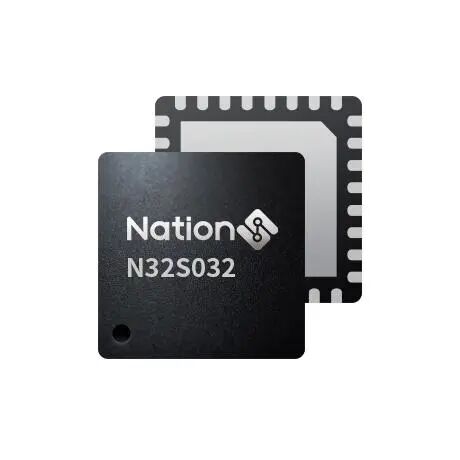
The N32S032 chip features an ARM-M0 secure processor core and an AMBA multi-bus architecture design. It is a high-performance 32-bit multi-purpose security chip developed by Nation Technology for electronic banking, e-commerce, e-government, and other mobile internet identity authentication and IoT security encryption applications. The N32S032 chip includes a hardware algorithm coprocessor that provides excellent performance for security algorithm modules such as DES/3DES, AES, SHA, RSA, ECC, and national commercial cryptography SM1/SM2/SM3/SM4. It also integrates a 12-bit 1Msps high-precision SAR ADC, a 10-bit DAC, a comparator, an RTC real-time clock, high-performance PWM, USB2.0 (FS), multiple SPI, UART, I2C, and ISO7816 application peripheral interfaces, making it easy to implement IoT and mobile internet security authentication solutions.
Key Features
System Functions
• CPU Core System
– ARM SC000 secure processor core (based on ARM Cortex-M0 architecture)
– Supports little-endian mode
– Supports Thumb/Thumb-2 instruction set
– 2KB iCache
– 3-stage pipeline, single-cycle (32×32) multiplication
– NMI + up to 32 physical interrupts, supports 4-level nesting
– Maximum operating frequency of 80MHz
• Timer
– Supports 5 channels of 32-bit Timer, Timer4 can be used to wake up from Standby mode
– Supports auto-load mode and pre-load mode
– Supports input capture/timing functions
– In capture mode, supports 5 independent input signals, with input signal sources configurable as GPIO, internal comparator, and USB_RCV signals
• WDT
– 1 WDT, timing clock source supports internal OSC 80MHz and external 12MHz/11.2896MHz
– Configurable timing time, maximum 2^32 timing clocks
– Supports interrupt and system reset functions
• DMA
– Supports 1 physical channel, 8 logical channels
– Logical channel priority can be configured, with round-robin arbitration for the same priority
– Supports source and destination address increment configuration
– Supports auto-load circular mode
– Supports maximum transfer length of 4095, with configurable bit width of 8/16/32
– Supports configurable transfer direction, supporting Memory <-> Memory, Peripheral <-> Memory, and Memory <-> Peripheral
• RTC
– Supports 1 real-time clock RTC, 32-bit counter
– Clock supports internal OSC 32.768KHz and external 32.768KHz crystal
– Supports ppm adjustment, with adjustment accuracy of 0.5ppm and adjustment range of +/-1024ppm
– RTC supports wake-up from PD/Standby mode, with configurable wake-up times of 62.5ms/125ms/250ms/0.5S/1S, etc., with a maximum timing of 4 hours
Storage Unit
• FLASH
– 320KB FLASH, configurable
– Supports page erase, page write, double word write, byte write, double word read, byte read operations
– Page size of 512Bytes
– Minimum erase/write cycles of 100,000 times @ 25℃
– Minimum data retention time of 10 years @ 25℃
– Read/write performance
– Double word read/byte read time < 35ns
– Double word write/byte write time < 30us
– Page write time < 2ms (1 write plus verification)
– Page erase time < 4ms (1 erase plus verification)
– Self-destruction time < 20ms
• SRAM
– 20KB general-purpose system SRAM
– 1KB Retention RAM
– 3KB PAE dedicated RAM
• Memory Protection Unit (MPU)
– Implements secure access control with different user permissions
– FLASH and SRAM access permission control
– ARAM area supports user-exclusive configuration
– Supports BOOT/COS/APP partition control, with a maximum of 2 APP user areas
Security Components
• RSA public key algorithm engine
• ECC public key algorithm engine
• National cryptography SM2 public key algorithm engine
• DES/3DES algorithm unit
– Supports ECB and CBC encryption modes
– Supports DES and TDES encryption/decryption operations
– TDES supports 2KEY and 3KEY modes
• AES algorithm unit
– Supports ECB and CBC encryption modes
– Supports 128bit/192bit/256bit key lengths
• National symmetric SM1/SM4 algorithm unit
– Supports ECB and CBC encryption modes
– Supports configurable round operations
• SHA1/SHA224/SHA256/SHA384/SHA512 algorithm unit
• National hash SM3 algorithm unit
• CRC
– Complies with ISO/IEC 3309 standard, supports polynomial X16+X15+X2+X0
– Supports CRC direction configuration for the data to be checked
– Initial value for cyclic redundancy calculation can be configured
– Supports DMA mode
• Security Protection
– Voltage anomaly detection, temperature anomaly detection, frequency anomaly detection, light anomaly detection
– Glue Logic, Active Layer (MESH), Passive Layer
– Reset glitch filtering, clock glitch filtering
– Memory address scrambling
– Data encryption in memory
– Memory integrity protection verification
– Memory access permission protection mechanism
– Complies with AIS32-P2 standard and national cryptography standard for true random number generator
– Symmetric algorithm (SM1/SM4/DES) hardware coprocessor designed to prevent DPA/SPA attacks
– Asymmetric algorithm (SM2/RSA/ECC) hardware coprocessor designed to prevent DPA/SPA/DFA attacks
– Self-test function
– Security design meets the secondary requirements of the National Cryptography Administration
– Security design meets the security requirements of EAL4+ certification from the National Information Security Testing Center
Communication Interfaces
• USB2.0 Full Speed Interface
– Complies with USB2.0 specification, supports Full Speed mode
– Supports no crystal mode
– Supports Control transfer, Interrupt transfer, Bulk transfer
– Supports Suspend mode
– Supports internal 1.5KΩ pull-up resistor on DP
– Supports 8 hardware endpoints, all endpoints with FIFO depth of 64 bytes
– 1 control endpoint (EP0/EP0)
– 3 interrupt endpoints (EP1/EP5/EP2)
– 4 BULK endpoints (EP3/EP6/EP4/EP7)
• PWM
– Supports 8 channels of PWM output
– Supports 6-channel three-phase PWM generator with complementary PWM output with dead time insertion, dead time programmable
– Supports single and continuous variable pulse width, adjustable duty cycle, can output all 1s or all 0s, with high and low level maximum width of 2^16 module clock cycles
– Supports single and continuous standard PWM output
– Maximum output frequency of 12MHz under external crystal; maximum 10MHz under internal clock
– Under external crystal, supports duty cycle variation of 1% at 0~20KHz output
– Supports DMA mode
• SCC (ISO7816 Master) Interface
– One master SCC controller
– Complies with ISO7816 specifications 1-3, supports T=0 and T=1 transmission protocols
– Supports 8 bytes of receive FIFO, 1 byte of transmit FIFO
– Supports automatic generation of parity bits and parity error detection
– Supports data retransmission (configurable, default is four times)
– Supports forward agreement (send LSB first) and reverse agreement (send MSB first)
– Supports output card clock, clock frequency configurable from 512KHz to 10MHz, supports stop card clock function, with configurable CLK IO state after stop card clock
– Minimum ETU supports 12 clocks, supports configurable frame transmission protection time, from 0 to 255 ETUs
– Supports card insertion and removal detection
• SCD (ISO7816 Slave) Interface
– One master SCD controller
– Complies with ISO7816-1/2/3 protocols, supports T=0/T=1
– Clock supports 500KHz–10MHz
– Supports 8 bytes of receive FIFO, 1 byte of transmit FIFO
– Supports fast transfer to receive mode
– Supports forward and reverse cards
– GuardTime protection time configurable
– Supports configurable number of error retransmissions
– Supports CRC module (Cyclic Redundancy Check), complies with ISO/IEC 3309 standard
• SPI Interface
– 2 independent SPI interfaces, supports Master and Slave software configuration
– Complies with SPI interface specifications
– Supports MSB and LSB transmission
– Chip select signal can be configured for software control
– Clock rate configurable, maximum rate supports 20Mbps
– Supports interrupt and polling modes
– As Master interface
– SPIM0 supports Single/Dual/Quad modes
– Supports configurable clock polarity and phase for data transmission and reception
– Supports Mode 0, 1, 2, 3
– Supports configurable output clock frequency
– As Slave interface
– Uses asynchronous clock design
– Supports Mode 0, 1, 2, 3
– Supports Standard mode
– Maximum frequency supports 20Mbps
• UART Interface
– 3 independent UART interfaces
– Complies with UART serial communication protocol specifications
– Asynchronous serial, full-duplex communication bus interface
– Two bus signals: TX data transmission, RX data reception
– Data transmission order: low bit (LSB) first, high bit (MSB) last
– Data structure: start bit, data bits, parity bit, and stop bit
– Clock source supports external crystal and internal OSC selection
– Receive FIFO length of 4 bytes, transmit FIFO length of 1 byte
– 2 channels support flow control CTS and RTS, can be disabled by software
– Output RTS is applied on the master side for reception, RTS low active indicates the other party can send data
– Input CTS is applied on the master side for transmission, CTS low active indicates the other party can receive data
– Maximum baud rate supports 921600bps
• I2C Interface
– 2 I2C interfaces, supports master-slave mode switching
– Slave address can be programmed and configured
– 1 byte transmit FIFO and 1 byte receive FIFO
– Supports DMA mode
– Maximum transmission rate supports 1Mbps
• GPIO
– Supports 30 configurable GPIOs
– GPIOs support pull-up/pull-down configuration, rising/falling edge, dual edge interrupts, and configurable trigger modes
– IO drive capability configurable, default not less than 4mA, maximum configurable to 18mA
– Supports GP0~GP15, a total of 16 IOs for Standby mode wake-up, supporting high and low level configuration
• ADC
– 1 channel 12Bit ADC
– Supports internal battery voltage detection channel and temperature sensor detection channel
– Supports up to 10 single-channel or 3 differential dual-end modes externally
– Supports maximum sampling rate of 1Msps
– Supports single sampling and continuous sampling
– Supports DMA mode
– Supports internal reference (default) and external reference applications
– Internal reference fixed at 1.2V
– External reference adjustable (range 0~VDD33)
– Supports built-in depth 4 Word, 32-bit width FIFO
• DAC
– Supports 1 channel 10bit DA converter
– Output voltage range: 0.2V—VREF-0.2V
– ENOB > 9.5bit, maximum sampling rate 400Ksps
– Data source for transmission supports UART/PWM, transmission rate determined by UART rate and PWM rate
– Built-in depth of 1 Word, 32-bit width asynchronous FIFO (valid bits 10bits)
– Supports DMA mode
• Comparator
– 1 general-purpose differential comparator
– Supports single-ended and differential modes
– Comparator output can be configured to output GPIO15, Capture, UART RX
– Supports built-in 1.65V bias
• Input Capture
– 5 independent input capture controllers
– Supports configurable input signal sources
– Supports glitch filtering
– Supports configurable single rising edge, single falling edge, rising edge or falling edge, capturing Counter count value
– Supports software clearing of Counter and continuing counting
Electrical Characteristics
• Maximum operating current (@VCC:3.3V/25℃): 35mA @ CPU 80MHz, PAE 80MHz
• Supports low power modes (@VCC:3.3V/25℃):
– PowerDown mode: 0.1uA (typical)
– PowerDown with 1K SRAM Retention & RTC work mode: 0.8uA (typical)
– Standby mode: 120uA (typical)
• Operating voltage: 1.8V~5.5V
• Operating temperature range: -25℃~85℃ (commercial grade), -40℃~85℃ (industrial grade)
• Storage temperature range: -40℃~125℃
• ESD: ±4KV (HBM model)
Applications
The N32S032 is a high-performance 32-bit multi-purpose security chip widely used in financial network security and payments, IoT security, vehicle networking security, industrial internet security, smart home security, security monitoring, and smart wearable secure payments.
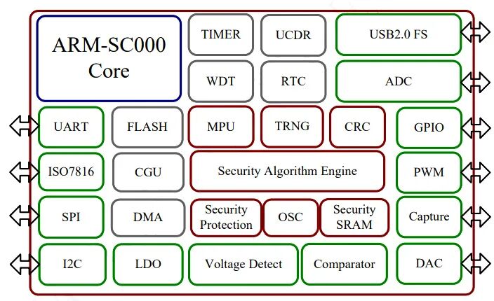
Structural Block Diagram
With its deep technical accumulation, ACROVIEW Technology’s self-developed AP8000 universal programmer is regarded as a benchmark-level programming solution in the industry. This device supports flexible one-to-one and one-to-eight configurations, while providing both online and offline working modes. It has also developed dedicated programming solutions for eMMC and UFS storage chips, fully meeting the bare chip offline programming and on-board programming needs for the entire series of chips from Nation Technology. The AP8000 consists of three core modules: host, baseboard, and adapter, and this modular design endows it with excellent compatibility and expandability. As a universal programming platform, the AP8000 can not only adapt to various programmable chips on the market but also, due to its stable and efficient performance, has become the core component of ACROVIEW’s automated IPS5800S programming system, efficiently handling large-scale chip programming tasks to meet mass production needs.The AP8000 host features flexible connectivity options, equipped with USB and NET interfaces, allowing for easy networking of multiple programmers. Through the networking function, users can easily achieve synchronized control of multiple programmers, efficiently conducting parallel programming operations. In terms of safety, the host is equipped with an intelligent safety protection circuit that can monitor the chip placement status and circuit connection in real-time. Once it detects abnormal conditions such as chip reverse insertion or short circuits, it will immediately trigger a power-off protection mechanism, fully safeguarding the safe operation of the chip and programmer. The host is internally equipped with a high-speed FPGA chip, significantly enhancing data transmission and processing efficiency, ensuring a smooth and efficient programming process. To enhance user convenience, the back of the host is equipped with an SD card slot, allowing users to store project files generated with the PC on the SD card and insert it into the slot. They can then complete file selection and loading for programming operations through the physical buttons on the programmer, achieving independent operation without a PC. This design not only reduces dependence on computer hardware configurations but also simplifies the setup process of the working environment, significantly enhancing operational flexibility.
In terms of expandability and compatibility, the AP8000 adopts a modular design of baseboard and adapter board, effectively expanding the functional boundaries of the host. Currently, this device has achieved support for all mainstream semiconductor manufacturers’ products, covering well-known brands such as Melexis, Intel, RICHTEK, indiemicro, Fortior Tech, etc. It supports a wide range of device types, including NAND, NOR, MCU, CPLD, FPGA, EMMC, etc., and is fully compatible with various industry-standard file formats such as Intel Hex, Motorola S, Binary, POF, providing users with a one-stop, all-scenario chip programming solution.
Company Introduction
About Nation Technology: Nation Technology (Nation) was established in 2000 as part of the national “909” integrated circuit special project. It is a leading enterprise in China’s security chips and general-purpose MCUs, a national high-tech enterprise, and has the first independent security chip attack and defense technology laboratory in the country, as well as a post-doctoral research workstation. Its main products include: security chips, general-purpose MCUs, trusted computing chips, smart card chips, contactless read-write chips, Bluetooth chips, RCC innovative products, etc., widely used in network security authentication, electronic banking, electronic certificates, mobile payments and mobile security, IoT, industrial networking and industrial control, smart home appliances and smart home IoT terminals, consumer electronics, motor drives, battery and energy management, smart metering, medical electronics, automotive electronics, security, biometrics, communications, sensors, and machine automation applications.
About ACROVIEW Technology:ACROVIEW Technology is a national-level specialized and innovative “little giant” enterprise engaged in the research, production, and sales of semiconductor chip testing and programming equipment. The company is committed to empowering the entire industry chain customers, including Fabless, IDM, OSAT, wafer fabs, and end-device enterprises, through innovative semiconductor testing technologies and solutions. ACROVIEW’s pioneering fully automatic aging test ABI (Auto Burn-In) system greatly enhances the aging test efficiency of customer chips and reduces the Per DUT testing cost. It also provides customers with equipment products and solutions for all stages from PSV, CP, FT, BI, SLT, to programming. We perfectly integrate the leading advantages of product technology, system-level expertise, and a globally laid-out R&D and sales service network to create value for customers to gain a competitive edge in the market.
Scan to follow us

ACROVIEW Technology Service Account

ACROVIEW Technology Subscription Account