Source: Semiconductor Industry Observation (ID: icbank)
Authors: By Pavan H Vora, Ronak Lad (Einfochips Pvt. Ltd.)
In 1958, Texas Instruments (TI) manufactured the first integrated circuit trigger using two transistors. Today’s chips contain over tens of billions of transistors. Memory that once supported an entire company’s accounting system has now transformed into a smartphone that people carry with them. This scale of growth is due to the continuous miniaturization of transistors and other improvements in silicon manufacturing processes. Throughout this development process, besides the continuous evolution of processes, transistors have also undergone several transformations. Before we enter a new generation of transistors, let’s review the development of previous generations of transistors.
The invention of the vacuum tube propelled the development of the electronics industry. These devices controlled the flow of electrons in a vacuum. However, after World War II, it was observed that the complexity and power consumption of these devices were significantly increasing due to the large number of discrete components. As a result, the performance of the devices continued to decline. One example is the Boeing B-29, which was composed of 300-1000 vacuum tubes during the war. Each additional component reduced its reliability and increased troubleshooting time.
A major breakthrough occurred in 1947 when John Baden, William Shockley, and Watter Brattain at Bell Labs introduced the first functional point-contact germanium transistor. In 1950, Shockley developed the first bipolar junction transistor (BJT). Compared to vacuum tubes, transistors are more reliable, power-efficient, and smaller in size. A transistor is a three-terminal device that can be viewed as an electrically controlled switch. One of the terminals serves as the control terminal. Ideally, if current is applied to the control terminal, the device acts as a closed switch between the two terminals; otherwise, it acts as an open switch. In 1958, Jack Kilby of Texas Instruments (TI) built the first integrated circuit, which consisted of two bipolar transistors connected on a piece of silicon, marking the beginning of the “Silicon Age”. Early ICs used bipolar junction transistors. One of the drawbacks of BJTs is the issues caused by higher static power consumption. This means that power is consumed even when the circuit is not switching. This limits the maximum number of transistors that can be integrated into a single silicon chip.
In 1963, Frank Wanlass and CTSah from Fairchild introduced the first logic gate, which used n-channel and p-channel transistors in a complementary symmetric circuit configuration. This is what we now call CMOS. Static power consumption is nearly zero.
Early ICs used NMOS technology because the NMOS process was relatively simple and inexpensive compared to CMOS technology and could pack more devices into a single chip. Intel released the first microprocessor in 1971.
Due to the higher static power consumption of NMOS transistors compared to CMOS, IC power consumption became a serious issue in the 1980s as thousands of transistors were integrated into a single chip. Due to characteristics such as low power consumption, reliable performance, and high speed, CMOS technology has been adopted in almost all digital applications, replacing NMOS and bipolar technologies.
In the following years, the scaling of CMOS and improvements in processing technology propelled continuous increases in circuit speed, as well as further enhancements in chip packaging density and the performance-cost ratio of microelectronics.
Here, we discuss Bulk-Si CMOS technology, the necessity and importance of scaling, their various impacts, and related solutions. We also address the physical scaling limits of any new materials used in transistor materials and advanced technology nodes. Today, due to various limitations encountered at the 32nm technology node, the industry is shifting towards SOI and FinFET, replacing planar transistors.
Here, we first discuss the basic structure, operation, and important terms related to the core unit of CMOS (i.e., MOSFET or simply MOS). The first successful MOS transistor used metal as the gate material, SiO2 (oxide) as the insulator, and semiconductor as the substrate. Therefore, this device is called a MOS transistor. A field-effect transistor (FET) is one where the gate turns on and off the transistor, with the electric field passing through the gate oxide.
Two types of MOS structures are evident based on the type of conductive channel: n-channel and p-channel MOS. Here, we will only outline the NMOS transistor, as the two transistors are essentially complementary.
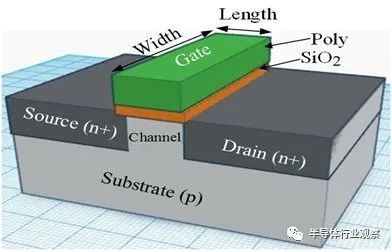
MOS transistors are four-terminal devices with terminals for drain, source, gate, and body (substrate). Figure 1 shows the 3D structure of NMOS. NMOS transistors are formed on a p-type silicon substrate (also called body). At the top central part of the device, a low-resistivity electrode is formed, which is separated from the body by an insulator. Typically, heavily doped n-type or p-type polysilicon is used as the gate material. Here, silicon dioxide (SiO2 or simply oxide) is used as the insulator. By injecting donor impurities on both sides of the substrate, the source and drain are formed. In Figure 1, these areas are indicated with n+, representing heavy doping of the donor impurities. This heavy doping results in low resistivity in these areas.
If the two n+ regions are biased at different potentials, the n+ region at the lower potential will act as the source, while the other will act as the drain. Therefore, the drain and source terminals can interchange based on the potentials applied to them. The region between the source and drain is called the channel with width W and length L, which plays an important role in determining the characteristics of the MOS transistor.
Figure 1. Structure of NMOS Transistor
B. Why Use Polysilicon as Gate Material?
In the early days of the semiconductor industry, aluminum was often used as the preferred gate material for MOS. However, later, polysilicon was preferred as the gate material. The two main reasons for the transition to polysilicon are described below.
The early MOS manufacturing process began with defining and doping the source and drain regions. Then, a gate mask defining the gate oxide region was used, which would subsequently form the aluminum metal gate.
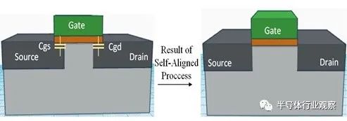
One of the major drawbacks of this manufacturing process is that if the gate mask is not aligned, parasitic overlapping input capacitances Cgd and Cgs will occur, as shown in Figure 2 (a). The capacitance Cgd is more harmful as it is a feedback capacitance. The switching speed of the transistor will be reduced due to Miller capacitance.
One solution to the misalignment of the gate mask is the so-called “self-aligned gate process.” This process starts by creating the gate region and then uses ion implantation to create the drain and source regions. The thin gate oxide beneath the gate acts as a mask for the doping process, preventing further doping below the gate region (channel). Therefore, this process allows the gate to be self-aligned with respect to the source and drain. As a result, the source and drain do not extend beneath the gate. This reduces Cgd and Cgs, as shown in Figure 2 (b).
Figure 2. (a) Cgd – Cgs Parasitic Capacitance, (b) Reduced Cgd and Cgs Due to Self-Aligned Process
The doping process for the source and drain requires very high-temperature annealing methods (>800°C). If aluminum is used as the gate material, it will melt at such high temperatures. This is because the melting point of Al is about 660 degrees Celsius. However, if polysilicon is used as the gate material, it will not melt. Therefore, using polysilicon gates allows for the self-aligned process. For Al-gates, this is not possible, leading to high Cgd and Cgs. Undoped polysilicon has a very high resistivity of about 108 ohm / cm. Therefore, it is doped in a way to reduce resistivity.
Another reason for choosing polysilicon is that the threshold voltage of the MOS transistor is related to the work function difference between the gate and the channel. Earlier, when the operating voltage was in the range of 3-5 volts, metal gates were used. However, as transistors shrank, this ensured that the operating voltage of the devices also decreased. Under these conditions, transistors with such high threshold voltages would not operate. Using metal as a gate material results in higher threshold voltages compared to polysilicon, as the composition of polysilicon is the same or similar to that of the bulk silicon channel. Additionally, since polysilicon is a semiconductor, its work function can be adjusted by varying the doping levels.
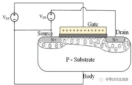
For MOS transistors, the gate voltage determines whether current will flow between the drain and source. Let’s look further. When a sufficiently positive Vgs voltage is applied to the gate of NMOS, positive charges will be placed above the gate, as shown in Figure 3. These positive charges will repel the minority carriers of the p-type substrate, namely holes from the substrate, leaving behind negative charge acceptor ions that create a depletion region. If we further increase Vgs, at certain potential levels, it will even attract electrons to the surface. Thus, a large number of electrons are attracted to the surface. This situation is called inversion, as the surface of the p-type body usually has a large number of holes, but the new surface has a large number of electrons.
The drain to body and source to body remain reverse biased. In Figure 3, the source to body maintains zero bias. Since the potential from drain to body is more positive than that from source to body, the reverse bias from drain to body is greater, resulting in a depletion layer beneath the drain region being deeper than that on the source side.
When a positive potential is applied across the drain to source, electrons flow from the source through the conductive channel and are discharged by the drain. Therefore, positive current Id flows from the drain to the source.
Figure 3. NMOS Transistor in Inversion Region
Driving Forces for Transistor Scaling
The demand for battery-powered portable devices has increased with the rise of applications such as cellular phones and laptops. The “basic requirement” for such applications is a smaller area, lower power consumption, and lower development costs. For these portable devices, power consumption is critical as the power provided by batteries is quite limited. Unfortunately, battery technology is not expected to increase battery storage capacity by more than 30% every five years. This is insufficient to handle the ever-increasing power requirements of portable devices.
In 1965, Gordon E. Moore predicted that the number of transistors in integrated circuits would double every two years. By making transistors smaller, more circuits can be manufactured on a silicon wafer, thus making circuits cheaper. Since less time is needed for current to flow from the drain to the source, reducing channel length accelerates the switching operation speed. In other words, smaller transistors lead to smaller capacitances. This results in reduced transistor delays. Since dynamic power is proportional to capacitance, power consumption is also reduced. This reduction in transistor size is referred to as scaling. Each time a transistor is scaled, we say a new technology node has been introduced. For example, 10nm, 7nm, and 5nm, etc. With each new generation of technology, this scaling improves cost, performance, and power consumption.
For long-channel devices, the “edge effects” along the four sides of the channel can indeed be neglected. For long-channel devices, the electric field lines are everywhere perpendicular to the channel surface. These electric fields are controlled by gate voltage and back gate voltage. However, for short-channel devices, the structure of the drain and source is closer to the channel, especially when the longitudinal electric field in the channel comes into play. The longitudinal electric field is controlled by the drain-source voltage. The longitudinal electric field is parallel to the direction of current flow. If the channel length is not greater than the sum of the depletion widths of the source and drain, the device is called a short-channel device.
In this section, we will discuss various adverse effects caused by two-dimensional potential distribution and high electric fields in short-channel devices.
A. Carrier Velocity Saturation and Mobility Degradation:
For lower electric field values, the drift velocity of electrons in the channel is proportional to the electric field. These drift velocities tend to saturate at high electric fields. This is called velocity saturation. For short-channel devices, the longitudinal electric field also tends to increase. At such high electric fields, velocity saturation occurs, which affects the IV characteristics of the MOSFET. It has been observed that for the same gate voltage, the saturation mode of the MOSFET is achieved at lower drain-source voltage values and with reduced saturation current.
Due to the higher vertical electric fields, carriers in the channel disperse from the oxide interface. This leads to a decrease in carrier mobility and a reduction in drain current.
B. Drain-Induced Barrier Lowering (DIBL):
Another short-channel effect known as DIBL refers to the reduction of threshold voltage at higher drain voltages. If the gate voltage is insufficient to cause surface inversion (i.e., gate voltage < threshold voltage), the carriers in the channel will face a barrier that prevents flow. By increasing the gate potential, we eliminate this barrier. However, for short-channel devices, this barrier is jointly controlled by Vgs and Vds. If the drain voltage increases, the depletion region size of the drain body increases and extends beneath the gate. Thus, even with Vgs below Vt, the channel barrier is reduced, allowing carriers (electrons) to flow between the source and drain. The concept of the drain lowering the channel barrier and reducing the threshold voltage is referred to as DIBL. This reduction of threshold voltage with channel length is called Vt roll-off. The current flowing under these conditions is referred to as subthreshold current (off-state current). Even in saturation mode, DIBL causes the drain current to increase with increasing drain bias.
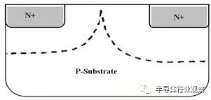
Punch-through is a severe barrier drop phenomenon. When the drain bias increases, the depletion region surrounding the drain can extend further towards the source in the case of the merging of the two depletion regions. This situation is referred to as punch-through. In this case, the drain current sharply increases, and the gate voltage loses control over the drain current. The punch-through effect increases with decreasing channel length. Due to punch-through, we cannot turn off the device, making it useless, as shown in Figure 4.
Figure 4. Punch-Through – Merging Two Depletion Regions
For smaller geometric devices, the electric field, especially near the drain, increases. As a result, electrons (carriers) gain a significant amount of energy, known as hot carriers.
Some of them gain nearly enough energy to cause impact ionization near the drain, generating new electron-hole pairs. As a result, it leads to current (Idb) from drain to body. A small number of hot electrons may tunnel through the oxide and collect themselves through the gate. Although some hot carriers may even damage the oxide, leading to a decline in device performance.
Controlling Short-Channel Effects
As observed in the previous section, if the channel length is smaller than the depletion region, short-channel effects can become unbearable. This limits further reduction of gate length. To mitigate these effects, the depletion region width should be reduced and the channel length correspondingly minimized. This can be achieved by increasing the channel doping concentration or increasing the gate capacitance, or both. The gate capacitance determines the gate’s control over the channel. Equation 1 indicates that the gate capacitance can be increased by scaling (reducing) the gate oxide layer thickness. It has been observed that devices with thinner gate oxides have reduced depletion widths, thus improving SCE characteristics.
COX = EOX / TOX (Equation-1)
COX: Gate oxide capacitance,
EOX: Electric field of the oxide
In the past few decades, for Intel’s process nodes, it has been observed that the ratio of oxide has been roughly proportional to channel length to limit SCE.
Innovations in Traditional Scaling
A. Moving Boosters: Strained Silicon Technology
One of the key scaling issues in nanoscale transistors is the reduction in mobility caused by larger vertical electric fields. There are many ways to enhance the performance and mobility of transistors. One method is to use germanium thin films in the channel, as germanium has a higher carrier mobility. Another method is to use strained silicon by introducing mechanical strain in the channel.
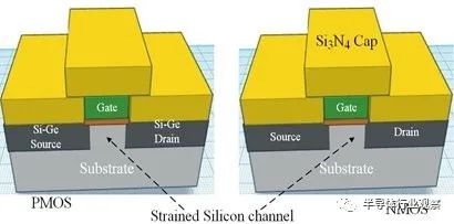
Strained silicon technology involves physically stretching or compressing silicon crystals in various ways to increase the mobility of carriers (electrons/holes) and enhance transistor performance. For example, when the channel is under compressive stress, the hole mobility of PMOS can be increased.
To create compressive strain in silicon channels, Si-Ge films are grown epitaxially to fill the source and drain regions. Si-Ge typically contains a mixture of 20% germanium and 80% silicon. The number of Si and Ge atoms is equal to the original Si atoms. Germanium atoms are larger than silicon atoms. Therefore, when force is applied, it pushes the channel and enhances hole mobility. Increasing the mobility of semiconductors can improve drive current and transistor speed.
Strained silicon technology for MOS transistors was first used by Intel in its 90nm process technology in 2003. In this technology node, the Si-Ge source-drain structure for PMOS transistors created compressive strain in the channel, resulting in a 25% increase in current. By adding a high-stress Si3N4 cover layer around the transistor, NMOS strain can increase the current by 10%.
B. Reducing Gate Leakage: High-K Dielectrics
The thickness of SiO2 (oxide) dielectrics should be proportional to its channel length. The 65nm node requires about 2.3nm (actual 1.6nm) of effective oxide thickness (EOT). However, if the oxide thickness is further reduced below this point, carrier phenomena of direct tunneling will dominate. As a result, gate leakage increases to unacceptable limits. Therefore, the limit for oxide thickness is about 1.6nm, set by gate-to-channel tunneling leakage (also known as quantum mechanical tunneling).
If we look at Equation 1, the only remaining option is to choose dielectric materials with high dielectric constants (K) to increase oxide capacitance. Since a thicker dielectric layer can be used, we can achieve higher gate oxide capacitance. This thicker layer results in less carrier tunneling. The breakthrough in gate oxides occurred in 2007 when Intel first introduced High-K dielectric materials (HfO2) in its 45nm mass production process. The dielectric constant of this material is about 25, which is six times higher than that of SiO2.
Figure 5. a) PMOS: Uniaxial Compressive Strain b) NMOS: Uniaxial Compressive Strain
EOT is given by Equation 3. Equation 3 indicates that a 6nm thick HfO2 provides about 1nm of EOT.
EOT = ( 3.9 X TOX ) / K (Equation-3)
EOT: Effective oxide thickness,
K: Dielectric constant of the material
C. Eliminating Polysilicon Depletion: Metal Gates
A depletion region forms at the interface of polysilicon and gate oxide. As device sizes continue to shrink, this depletion of polysilicon becomes larger, and a significant portion of the equivalent oxide thickness will limit the capacitance of the gate oxide. The negative impact of polysilicon depletion is due to the reduction in charge density of the inversion layer and the degradation of device performance. Therefore, in addition to the thickness of the gate oxide, the thickness of the polysilicon depletion layer also needs to be minimized.
Moreover, due to effects such as threshold voltage pinning and photon scattering, polysilicon gates may also be incompatible with high-K dielectrics, making it difficult to achieve low threshold voltages and reducing channel mobility.
One solution to eliminate polysilicon depletion effects is to use metal gates instead of polysilicon gates. Metal gates can eliminate polysilicon depletion effects and also allow the use of high-K dielectrics.
Intel first adopted high-K dielectrics and metal gate technology at the 45nm node. NMOS and PMOS use different metals because NMOS and PMOS require different work functions.
The transistor process flow begins with the deposition of high-K dielectrics and pseudo-polysilicon. After a high-temperature annealing process, interlayer dielectrics are deposited and polished to expose the polysilicon. Then, the pseudo-polysilicon is removed. Finally, PMOS is deposited in the gate trench, followed by the deposition of NMOS work function metal.
For conventional MOS structures, as channel lengths shrink, the gate cannot fully control the channel, which is undesirable. One of its effects is to lead to more subthreshold leakage from drain to source, which is unfavorable from a power consumption standpoint. In traditional MOS, the gate cannot control the leakage path, which is far from the gate. Various MOS structures can be used to improve this, allowing transistors to scale beyond the conventional MOS scaling limits. In this section, we will discuss two new MOS structures, namely SOI and FinFET. The primary goal of both structures is to maximize gate-to-channel capacitance and minimize drain-to-channel capacitance.
A. Silicon on Insulator (SOI):
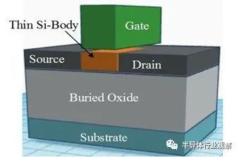
The main difference between conventional MOS structures and SOI MOS structures is that SOI devices have a buried oxide layer, which isolates the body from the substrate. As shown in Figure 7, SOI transistors are planner devices.
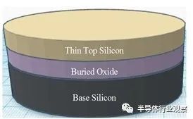
Besides the starting silicon wafer, the manufacturing process of SOI MOS is similar to that of bulk MOS (conventional MOS). SOI wafers have three layers: 1. A thin silicon surface layer (where the transistor is formed). 2. An insulating material layer. 3. A supporting or “handling” silicon wafer.
The fundamental idea behind the buried oxide layer is that it will reduce parasitic junction capacitance. The smaller the parasitic capacitance, the faster the transistor operates. This provides higher performance. Due to the BOX layer, there are no extra leakage paths away from the gate. This leads to lower power consumption.
Depending on the state of the thin body during operation, SOI devices can be classified into partially depleted (PD) SOI and fully depleted (FD) SOI. Compared to PD SOI, FD SOI has a very thin self-structure, thus fully depleting itself during operation. This FD SOI is also known as ultra-thin SOI. For PD SOI, the body thickness is between 50 nm to 90 nm. For FD SOI, the body thickness is about 5 nm to 20 nm.
Figure 7. Structure of SOI FET
Advantages of SOI Devices:
-
Due to the insulating layer, the parasitic capacitance of the drain/source is reduced. Therefore, the device has lower delay and dynamic power consumption compared to bulk CMOS.
-
Due to the insulating layer, the threshold voltage has less dependence on back-gate bias compared to bulk CMOS. This makes SOI devices more suitable for low-power applications.
-
SOI devices have better subthreshold characteristics, resulting in lower leakage currents.
-
SOI devices do not have latch-up issues.
Disadvantages of SOI Devices:
-
One disadvantage of PD SOI devices is that they are affected by history. In PD SOI, as the body becomes thicker, the floating body effect becomes significant. Therefore, the body voltage depends on the previous state of the device. This floating body voltage can alter the threshold voltage of the device. This may lead to severe mismatches between two identical transistors.
-
Another issue with SOI devices is self-heating. In SOI devices, the active thin film is located on top of the oxide, which is a good insulator. During operation, the power consumed in the active region cannot dissipate easily. As a result, the thin body temperature rises, reducing device mobility and current.
-
One of the challenges of FD SOI is the difficulty in manufacturing ultra-thin SOI wafers.
The concept of FinFET was proposed in 1999 by Morris Chang, the former CTO of TSMC, and his team at Berkeley University, and the concept of UTB-SOI (FD SOI) was proposed in 2000. The main principle of these two structures is the thin body, allowing better gate control. The body is very thin, about 10nm or shorter. Therefore, there are no leakage paths away from the gate. The fin structure can effectively control leakage.
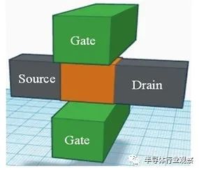
They proposed that the basic structure of FinFET would be a channel controlled from one side by multiple channels. One of the double-gate structures is shown in Figure 8.
Figure 8. Double Gate Structure
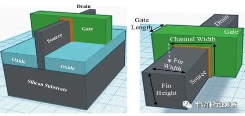
Modern FinFETs are 3D structures, as shown in Figure 9, also known as tri-gate transistors. FinFETs can be realized on bulk silicon or SOI wafers. This FinFET structure consists of thin (vertical) fins of silicon on the substrate. The gate wraps around the channel, allowing excellent control from three sides of the channel. This structure is referred to as FinFET because its Si body resembles a fish’s dorsal fin.
Figure 9. Fin-FET Structure
In bulk MOS (planar MOS), the channel is horizontal. In FinFET, the channel is vertical. Therefore, for FinFET, the height of the channel (fin) determines the width of the device. The ideal width of the channel is given by Equation 4.
Width of Channel = 2 X Fin Height + Fin Width (Equation-4)
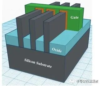
The drive current of FinFET can be increased by increasing the width of the channel (i.e., by increasing the height of the fin). We can also increase the device drive current by constructing multiple parallel fins connected together, as shown in Figure 10. This means that for FinFET, arbitrary channel widths are not possible, as it is always a multiple of the fin height. Therefore, the effective width of the device becomes quantized. In planar devices, the drive strength of the device can be freely chosen by changing the channel width.
Figure 10. Multi-Fin FinFET Structure
In traditional MOS, dopants are inserted into the channel to reduce various short-channel effects (SCE) and ensure high Vth. In FinFET, the gate structure wraps around the channel, and the body is thin, providing better SCE, thus channel doping becomes optional. This means that FinFET is less affected by variations caused by dopants. Low channel doping also ensures better mobility of carriers inside the channel. Therefore, higher performance. One thing to note here is that both FinFET and SOI technologies have introduced “body thickness” as a new scaling parameter.
FinFET technology offers numerous advantages over bulk CMOS, such as higher drive current for a given transistor footprint, leading to higher speeds, lower leakage, lower power consumption, and no random doping fluctuations, thus enhancing the mobility and scalability of transistors beyond 28nm, with TSMC also applying this transistor technology to its 5nm chips.
Both FinFET and SOI structures have better gate control and lower threshold voltages with less leakage. However, as we move to lower technology nodes (e.g., below 10nm nodes), leakage issues begin to resurface. This leads to many other problems such as threshold flattening, increased power density, and heat dissipation. FinFET structures are less efficient in heat dissipation as heat can easily accumulate on the fins. Unlike other design rules (such as manufacturability design), these concerns may lead to a new class of design rules – thermal design.
As these devices approach their limits, the industry is working collaboratively to provide potential solutions, including modifying device structures and replacing existing silicon materials with new materials. These include carbon nanotube (CNT) FETs and GAA, which are current hot topics.
Editor: Xiao Huibing