Word count: 9449, reading time approximately 48 minutes
ASICs vs. FPGAs: A Comprehensive Comparison
As key components in modern computing, the choice between ASICs and FPGAs is significant, highlighting the importance of understanding their unique advantages and trade-offs in an ever-evolving digital landscape.
Introduction
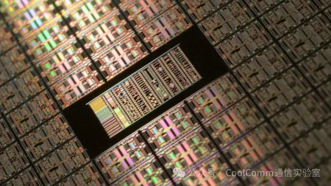
ASICs (Application-Specific Integrated Circuits) and FPGAs (Field-Programmable Gate Arrays) are two types of semiconductor devices used for different purposes in the electronics field. ASICs are custom-designed for specific applications, providing high performance and efficiency, while FPGAs are reprogrammable devices that offer flexibility and rapid prototyping capabilities. The choice between these two technologies depends on various factors, such as performance requirements, power consumption, cost, design flexibility, and time to market.
This article will provide a comprehensive comparison of ASICs and FPGAs, exploring their respective advantages and disadvantages, and offering guidance on when to choose one technology over the other. By understanding the key differences between these devices, engineers and designers can make informed decisions that best suit their project needs and constraints.
What is an ASIC?
Definition and Overview
An ASIC is a dedicated semiconductor device and circuit designed to perform a specific function or set of functions. Unlike general-purpose processors such as CPUs and GPUs, ASICs are customized according to the requirements of specific applications, achieving optimized performance and power efficiency. They are typically used in high-volume products where the cost of custom design can be justified by the benefits of improved performance, reduced power consumption, and smaller size.
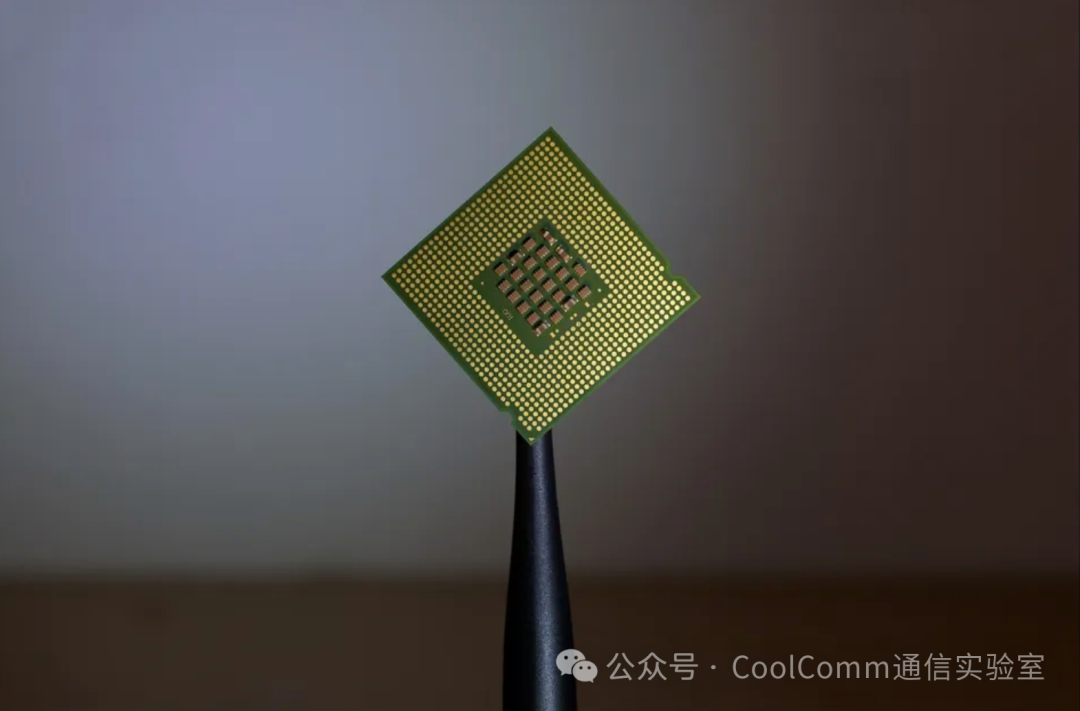
The manufacturing process of ASICs is called photolithography, where the layout of custom transistors and other components is etched onto a silicon wafer. This layout is designed to achieve the desired functionality of the ASIC, which can range from simple logic gates to complex digital signal processing circuits. The manufacturing process of ASICs is time-consuming and expensive, involving multiple steps such as mask creation, wafer fabrication, and packaging. However, once the initial investment is made, the unit cost of ASICs decreases significantly as production volume increases.
ASIC Design Process
The ASIC design process consists of several stages, each with its own tasks and challenges. The main stages include system specification definition, design, verification, manufacturing, and testing.
- • System Specification Definition: The first step in the ASIC design process is to define the system requirements and specifications. This involves determining the desired functionality, performance targets, power constraints, and other limitations. Engineers and designers collaborate to create a detailed specification document that serves as the blueprint for the ASIC design.
- • Design: The design phase involves translating the system specifications into a functional ASIC layout. This process typically begins with high-level architectural design, determining the overall structure and organization of the ASIC. Next, a logic synthesis converts the high-level description into a gate-level netlist. Various techniques (such as technology mapping and layout) are then used to optimize the netlist for area, power, and performance. Finally, the routing process creates the layout, connecting the gates and components on the silicon wafer. The tape out process of the ASIC marks the end of the design phase, which is critical as no changes can be made after manufacturing.
- • Verification: Verification is a crucial stage in the ASIC design process as it ensures that the design meets the system specifications and is error-free. This stage involves simulating the ASIC design using test vectors to check for correctness in functionality, timing, and power consumption. Verification can be performed at different levels of abstraction, from high-level functional verification to low-level gate-level simulation. Formal verification methods (such as model checking and theorem proving) can also be employed to prove the correctness of the design.
- • Manufacturing: Once the design is verified, it is sent to a semiconductor foundry for manufacturing. The manufacturing process involves creating a series of photomasks that represent different layers of the ASIC layout. These photomasks are used to pattern the silicon wafer through a series of steps (including photolithography, etching, and deposition). The completed wafers are cut into individual ASIC chips and packaged for use in electronic systems.
- • Testing: The final stage of the ASIC design process is testing, which ensures that the manufactured chips meet the specified performance, power, and reliability requirements. Testing involves applying a set of test vectors to the ASIC and measuring its outputs to verify that the functionality is correct. Additionally, manufacturing defect tests (such as stuck-at faults and bridging faults) are performed to ensure the quality of the manufactured chips. Once the ASIC passes all tests, they can be integrated into electronic systems and deployed in real-world environments.
Before starting ASIC development, it is essential to assess its necessity. Conducting a return on investment (ROI) analysis is crucial to ensure that the benefits to the company and customers outweigh the investment risks. For example, if the current PCB cost is $20, and a potential ASIC could reduce it to $2, the relationship between the break-even point and the ASIC development cost needs to be considered.
It is vital to verify whether the envisioned ASIC functionality and performance are achievable. Many ASIC vendors offer feasibility study services to review your specifications and determine the project’s feasibility. A detailed ASIC specification document is crucial for obtaining accurate price estimates from design firms.
Advantages of ASICs
Having understood what ASICs are and their common use cases, it is essential to delve into their unique advantages. These advantages make them the preferred technology in many applications, justifying the investment in custom development. Let’s explore these advantages in detail:
- • High Performance: One of the main advantages of ASICs is their high performance. Since they are custom-designed for specific applications, they can be optimized for maximum efficiency and speed. ASICs typically outperform general-purpose processors (such as CPUs and GPUs) in their target applications due to their custom architecture and dedicated hardware resources.
- • Low Power Consumption: ASICs are designed with power efficiency in mind, making them suitable for applications where power consumption is critical. By optimizing the design for specific functions, ASICs can reduce the number of active components, leading to lower power consumption compared to general-purpose processors. This is particularly important for battery-powered devices (such as smartphones and IoT sensors), where energy efficiency is a key concern.
- • Small Size: ASICs can be designed with compact layouts, resulting in smaller sizes compared to general-purpose processors. This is advantageous for space-constrained applications (such as wearable devices and embedded systems). Smaller sizes also enable more efficient heat dissipation and better thermal performance.
- • Intellectual Property Protection: Custom ASIC designs can provide a higher level of intellectual property (IP) protection compared to off-the-shelf components. By implementing proprietary algorithms and functionalities directly into hardware, companies can safeguard their IP from reverse engineering and unauthorized use.
- • Cost-Effectiveness in Mass Production: Although the initial investment for ASIC design and manufacturing can be high, the unit cost decreases significantly as production volume increases. This makes ASICs cost-effective for high-volume products, where the advantages of improved performance, reduced power consumption, and smaller size outweigh the upfront costs.
- • Multi-Functional Integration: ASICs can integrate multiple functions and components into a single chip, reducing the need for additional components and simplifying the overall system design. This can lower system complexity, reduce manufacturing costs, and improve reliability.
Disadvantages of ASICs
While ASICs have significant advantages in certain cases, it is also essential to consider their limitations during the design and decision-making process. Understanding these disadvantages is crucial for assessing whether ASICs are the right choice for a given application. Let’s explore these limitations in detail:
- • High Initial Costs: The design and manufacturing of ASICs require substantial upfront investment, including costs for design tools, engineering resources, and manufacturing setups. These initial costs can be prohibitive for small companies or budget-constrained projects, making ASICs less attractive for low-volume production.
- • Long Development Cycles: The ASIC design process is time-consuming, often taking months or even years to complete. In fast-paced industries, rapid product development and time to market are critical, and this longer development cycle can be a disadvantage.
- • Poor Flexibility: Once an ASIC is designed and manufactured, its functionality is fixed and cannot be changed without redesigning and manufacturing a new chip. This lack of flexibility can be a drawback for applications where requirements may change over time or where updates to functionality are needed.
- • Obsolescence Risk: Due to the rapid pace of technological advancements in the semiconductor industry, ASICs can become obsolete relatively quickly. For companies investing in custom ASIC development, the risk of obsolescence can be a concern, as if the technology becomes outdated before the end of the product lifecycle, the return on investment may diminish.
- • Design Complexity: The design of ASICs is complex and requires expertise and experience in semiconductor design, manufacturing, and testing. This complexity can be a barrier for companies without in-house expertise or access to external resources, making the development of custom ASIC solutions more challenging.
- • Manufacturing Yield and Reliability: The manufacturing process of ASICs is intricate and precise, which can lead to yield and reliability issues. Defects during the manufacturing process can result in chips that do not function correctly or have reduced performance, increasing the overall costs and risks associated with ASIC development.
Examples of ASICs
Due to their custom design, ASICs are commonly used in various devices and systems where performance, power efficiency, and size are critical. Here are some common examples of ASIC chips:
- • Cryptocurrency Mining Hardware: ASICs are widely used in cryptocurrency mining as they can be optimized for specific hashing algorithms (such as Bitcoin’s SHA-256), making them more efficient than general-purpose computing devices.
- • Consumer Electronics: Devices such as smartphones, tablets, smart TVs, and gaming consoles often contain ASICs. These chips are custom-designed for specific functionalities of each device, such as graphics rendering, audio processing, and cellular communication.
- • Telecommunications and Networking Equipment: ASICs are used in various networking devices, such as routers, switches, and modems, to efficiently handle high-speed data processing tasks.
- • Automotive Systems: ASICs are used in various automotive systems, including advanced driver-assistance systems (ADAS), engine control units, and infotainment systems. They provide the necessary computing and control capabilities while meeting the strict standards for reliability and robustness in automotive applications.
- • Medical Devices: In devices such as hearing aids, pacemakers, and imaging systems (like MRI machines), ASICs provide dedicated functions with low power consumption, which is a critical feature for battery-powered devices.
- • Industrial Control Systems: ASICs are commonly used in industrial control systems for specific tasks such as motor control, power management, and sensor data processing, providing robust and reliable operation in challenging industrial environments. ASICs can act as microcontrollers tailored for specific applications, ensuring optimal performance.
Remember, the commonality among all these examples is the need for optimization and efficient performance for specific tasks or sets of tasks, which justifies the cost and effort of developing custom ASICs.
What is an FPGA?
Definition and Overview
An FPGA is a semiconductor device that can be reprogrammed to implement various digital circuits and functions. Unlike ASICs (fixed-function devices), FPGAs offer flexibility and adaptability, allowing designers to modify the functionality of the device after manufacturing. This makes FPGAs an attractive choice for rapid prototyping, proof-of-concept development, and applications where design changes are anticipated.
FPGAs consist of programmable logic blocks and interconnects that can be configured to implement a wide range of digital circuits, from simple logic gates to complex digital signal processing systems. The programmable logic blocks contain lookup tables (LUTs), flip-flops, and other components that can be used to create custom logic functions. The interconnects provide the routing infrastructure to connect the logic blocks, enabling the implementation of larger and more complex circuits. Notably, FPGAs from vendors like AMD-Xilinx can be equipped with flash memory, allowing them to retain data even without power.
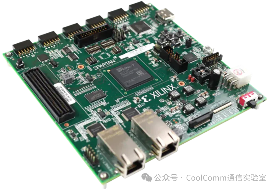
FPGA programming is typically done using hardware description languages (HDLs) such as VHDL or Verilog, allowing designers to describe the expected functionality of the device at a higher level of abstraction. The HDL code is then synthesized into a bitstream, which is loaded onto the FPGA to configure the programmable logic blocks and interconnects. This process can be repeated as needed to update or modify the FPGA’s functionality, providing a high degree of design flexibility and adaptability.
FPGA Design Process
Compared to the ASIC design process, the FPGA design process is generally more flexible, allowing for iterative testing and modifications. The FPGA design process involves several stages, including system specification definition, design input, synthesis, place and route, and verification.
- • System Specification Definition: Similar to the ASIC design process, the first step in FPGA design is to define the system requirements and specifications. This involves determining the desired functionality, performance targets, power constraints, and other limitations. Engineers and designers collaborate to create a detailed specification document that serves as the blueprint for the FPGA design.
- • Design Input: In this phase, designers create a high-level description of the expected functionality using HDL (such as VHDL or Verilog). This HDL code describes the behavior of the digital circuit to be implemented on the FPGA. Alternatively, designers can use schematic input or graphical design tools to create the design.
- • Synthesis: The HDL code or schematic is then synthesized into a gate-level netlist, which represents the digital circuit in terms of logic gates and flip-flops. The synthesis process involves mapping the high-level design description to the specific resources available on the target FPGA, such as lookup tables (LUTs), registers, and digital signal processing (DSP) modules.
- • Place and Route: The next phase is the place and route stage, which assigns the synthesized logic elements to specific locations on the FPGA and determines the interconnect routing between them. This process aims to optimize for area, performance, and power while considering the constraints and requirements specified in the system specifications.
- • Verification: Verification is a critical stage in the FPGA design process as it ensures that the design meets the system specifications and is error-free. This stage involves simulating the FPGA design using test vectors to check for correctness in functionality, timing, and power consumption. Verification can be performed at different levels of abstraction, from high-level functional verification to low-level gate-level simulation. Additionally, in-circuit testing and hardware debugging can be performed using FPGA development boards and debugging tools.
Once the design is verified, the final bitstream is generated and loaded onto the FPGA to configure the programmable logic blocks and interconnects. The FPGA can then be integrated into the target system and deployed in real-world environments. If design changes are needed, the FPGA can be reprogrammed using the updated bitstream, providing a high degree of flexibility and adaptability.
Advantages of FPGAs
FPGAs offer a unique set of advantages, particularly in terms of flexibility and adaptability. Let’s explore these advantages in more detail:
- • Design Flexibility: One of the main advantages of FPGAs is their design flexibility. FPGAs can be reprogrammed to implement different digital circuits and functions, allowing designers to modify the functionality of the device after manufacturing. This design flexibility makes FPGAs an attractive choice for rapid prototyping, proof-of-concept development, and applications where design changes are anticipated.
- • Short Time to Market: Compared to the ASIC design process, the FPGA design process is typically faster, as it does not require time-consuming manufacturing and fabrication steps. This shorter time to market enables companies to respond more quickly to market changes and technological trends, providing a competitive advantage in fast-paced industries.
- • Lower Non-Recurring Engineering (NRE) Costs: Unlike ASICs, which require significant upfront investment for design and manufacturing, FPGAs have lower NRE costs. This makes FPGAs a more cost-effective choice for low-volume production or budget-constrained projects.
- • Field Upgradability: FPGAs can be reprogrammed in the field, allowing for updates and modifications without the need to replace hardware. This field upgradability can reduce maintenance costs and extend the lifespan of electronic systems.
- • Parallel Processing Capability: FPGAs are inherently parallel devices, with multiple programmable logic blocks that can operate independently and simultaneously. This parallel processing capability makes FPGAs excel in applications requiring high-speed data processing, such as digital signal processing, image processing, and cryptography.
- • Ability to Adapt to New Technologies: FPGAs can be reprogrammed to support new technologies and standards as they emerge, making them a future-proof solution for applications that require continuous updates and enhancements. This adaptability can help companies maintain a competitive edge and extend the lifecycle of their products. FPGAs perform exceptionally well in projects requiring multiple interfaces due to their reconfigurability.
- • Lower Obsolescence Risk: Due to their reprogrammable nature, FPGAs have a lower risk of obsolescence compared to ASICs. As technology evolves, FPGAs can remain relevant and useful by updating their functionalities, thereby extending their lifespan.
Disadvantages of FPGAs
Despite the many compelling advantages of FPGAs, there are also some inherent drawbacks. These drawbacks include:
- • Lower Performance: Compared to ASICs, FPGAs generally have lower performance because they are not optimized for specific applications. The programmable nature of FPGAs introduces overhead in terms of area, power, and performance, making them less suitable for applications with extremely high efficiency and speed requirements.
- • Higher Power Consumption: Due to their programmable architecture, FPGAs typically consume more power than ASICs. The additional power consumption is due to the configurable logic blocks, interconnects, and other resources within the FPGA that provide flexibility. This higher power consumption can be a disadvantage in applications where energy efficiency is critical.
- • Larger Size: Compared to ASICs, FPGAs generally have a larger size because they require additional resources to achieve programmability. This larger size can be a drawback in applications with space constraints or where compact designs are needed.
- • Higher Unit Costs: Although FPGAs have lower NRE costs, their unit costs are typically higher than ASICs, especially in high-volume production. The higher unit costs of FPGAs are due to their need for additional programmable resources and lower integration levels compared to custom ASIC designs.
- • Design Complexity: FPGA design can be complex, requiring expertise in hardware description languages (HDLs), synthesis tools, and place-and-route algorithms. This complexity can be a barrier for companies without in-house expertise or access to external resources, making the development of FPGA-based solutions more challenging.
- • Limited Resources: The number of programmable logic blocks, interconnects, and other resources in an FPGA is limited, which may constrain the complexity and functionality of designs that can be implemented on a single device. In some cases, designers may need to distribute designs across multiple FPGAs or use larger, more expensive devices to meet their needs.
Comparing ASICs and FPGAs
The debate between FPGAs and ASICs primarily revolves around the trade-off between design flexibility and performance optimization. However, there are many other parameters to consider when choosing between the two.
Performance
When comparing the performance of ASICs and FPGAs, it is important to consider the specific application and requirements. Generally, ASICs outperform FPGAs because they are custom-designed for specific functions. Since ASICs are tailored for specific functionalities, they can be designed for maximum efficiency and speed, providing better performance for specific applications.
FPGAs, on the other hand, sacrifice performance for flexibility. The programmable nature of FPGAs introduces overhead in terms of area, power, and performance, as their configurable logic blocks and interconnects are not as efficient as the custom-designed components in ASICs.
However, it is worth noting that as FPGA technology advances, the performance gap between ASICs and FPGAs is narrowing. In recent years, FPGAs have made significant strides in logic density, clock speeds, and on-chip resources. In some cases, the performance of FPGAs can rival that of ASICs, especially when considering the use of dedicated hardware blocks (such as DSP units and embedded memory).
Both ASICs and FPGAs can integrate analog components, such as analog-to-digital converters (ADCs), allowing their functionality to extend beyond pure digital tasks. In certain cases, FPGAs can achieve performance levels comparable to ASICs, particularly when using dedicated hardware blocks and optimized design techniques.
The choice between ASICs and FPGAs in terms of performance depends on the specific application requirements and the trade-offs between performance, flexibility, and cost. For applications requiring the highest efficiency and speed, ASICs may be the preferred choice. However, for applications needing rapid prototyping, design flexibility, or the ability to adapt to changing requirements, FPGAs can provide a viable alternative with competitive performance levels.
Power Consumption
Power consumption is a critical factor when comparing ASICs and FPGAs, as it affects the overall efficiency of electronic systems, battery life, and thermal performance. Generally, ASICs have lower power consumption than FPGAs because they are custom-designed for specific applications.
ASICs are tailored for specific applications, allowing for high levels of optimization in power consumption. By reducing the number of active components and customizing the design for target functionalities, ASICs can achieve lower power consumption than general-purpose processors and FPGAs. This is particularly important for battery-powered devices and applications sensitive to energy efficiency, where power consumption is a key concern.
FPGAs tend to have higher power consumption due to their programmable nature. The configurable logic blocks, interconnects, and other resources within FPGAs introduce overhead in terms of power consumption. Additionally, FPGAs often operate at lower clock frequencies, which can lead to higher dynamic power consumption in certain applications.
However, it is worth noting that as FPGA technology advances, their power efficiency has improved significantly. Newer FPGA devices feature lower static power consumption, more efficient interconnects, and advanced power management capabilities. In some cases, FPGAs can achieve power levels comparable to ASICs, especially when using dedicated hardware blocks and optimized design techniques.
When comparing ASICs and FPGAs in terms of power consumption, it is important to consider the specific application requirements and the trade-offs between power efficiency, flexibility, and cost. For applications requiring the lowest power consumption, ASICs may be the preferred choice. However, for applications needing design flexibility or the ability to adapt to changing requirements, FPGAs can provide a viable alternative with competitive power levels.
Cost
Cost is an important factor when comparing ASICs and FPGAs, as it affects the overall affordability of projects and return on investment. The cost differences between these two technologies can be attributed to factors such as non-recurring engineering (NRE) costs, unit costs, and manufacturing complexity.
- • Non-Recurring Engineering Costs: ASICs have high NRE costs due to the need for custom design, manufacturing, and fabrication setups for each unique design. These upfront costs can be prohibitive for small companies or budget-constrained projects, making ASICs less attractive for low-volume production. In contrast, FPGAs have lower NRE costs because they do not require custom manufacturing and can implement different designs using the same equipment through reprogramming.
- • Unit Costs: Although FPGAs have lower NRE costs, their unit costs are typically higher than ASICs, especially in high-volume production. The higher unit costs of FPGAs are due to their need for additional programmable resources and lower integration levels compared to custom ASIC designs. However, for low-volume production or projects with rapidly changing demands, the higher unit costs of FPGAs may be offset by their lower NRE costs and design flexibility.
- • Manufacturing Complexity: The manufacturing process of ASICs is more complex and time-consuming than that of FPGAs, which can impact the overall cost and delivery time of projects. ASIC manufacturing involves multiple steps, such as mask creation, wafer fabrication, and packaging, which can lead to higher costs and longer delivery times. FPGAs can be purchased off-the-shelf and programmed as needed, reducing manufacturing complexity and delivery times.
When comparing ASICs and FPGAs in terms of cost, it is important to consider the specific application requirements and the trade-offs between upfront investment, unit costs, and design flexibility. For high-volume production or applications requiring the lowest unit costs, ASICs may be the preferred choice. However, for low-volume production or projects with rapidly changing demands, FPGAs can provide a more cost-effective alternative with lower NRE costs and greater design flexibility.
Design Flexibility
Design flexibility is a key factor when comparing ASICs and FPGAs, as it affects the ability to adapt to changing requirements and accommodate new features or functionalities. The differences in design flexibility between these two technologies primarily stem from their respective architectures and programmability.
- • ASICs: As custom-designed devices, ASICs have limited design flexibility once they are manufactured. Any changes to the functionality or features of an ASIC require a new design and manufacturing process, which can be both time-consuming and costly. This lack of flexibility can be a disadvantage for applications where requirements may change over time or where the ability to update functionality is important. However, the custom nature of ASICs allows for highly optimized designs that can provide better performance, power efficiency, and size compared to FPGAs.
- • FPGAs: In contrast, FPGAs offer high design flexibility due to their programmable architecture. The configurable logic blocks and interconnects within FPGAs can be reprogrammed to implement different digital circuits and functions, allowing designers to modify the functionality of the device after manufacturing. This flexibility makes FPGAs an attractive choice for rapid prototyping, proof-of-concept development, and applications where the ability to adapt to new technologies and standards is crucial.
When comparing ASICs and FPGAs in terms of design flexibility, it is important to consider the specific application requirements and the trade-offs between performance, power efficiency, and adaptability. For applications requiring the highest level of optimization and fixed functionality, ASICs may be the preferred choice. However, for applications needing design flexibility, the ability to adapt to changing requirements, or rapid prototyping capabilities, FPGAs can provide a more suitable solution.
Time to Market
Time to market is an important factor when comparing ASICs and FPGAs, as it affects the competitiveness and success of products in the market. The primary differences in time to market between ASICs and FPGAs stem from their respective design, manufacturing, and verification processes.
- • ASICs: The ASIC design process is time-consuming, often taking months or even years to complete. This longer development time includes design, verification, manufacturing, and testing phases, which can be a disadvantage in fast-paced industries where rapid product development and time to market are critical. Additionally, any changes to ASIC designs require a new manufacturing process, further extending the time to market.
- • FPGAs: In contrast, the FPGA design process is typically faster than the ASIC design process, as it does not require time-consuming manufacturing and fabrication steps. FPGAs can be purchased off-the-shelf and programmed to implement the desired functionality, allowing for rapid prototyping and shorter development cycles. Additionally, design changes can be implemented by reprogramming the FPGA without the need for a new manufacturing process. This shorter time to market enables companies to respond more quickly to market changes and technological trends, providing a competitive advantage in fast-paced industries.
Below is a comparison table of ASICs and FPGAs, providing a detailed overview of their respective characteristics and applications.
| Comparison Point | ASIC | FPGA |
| Design Flexibility | Limited flexibility once manufactured; changes require redesign and manufacturing | High flexibility due to programmability; modifications can be made post-manufacturing; suitable for rapid prototyping and adaptive designs |
| Performance | Higher performance due to custom design; optimized for specific applications | Lower performance due to reconfigurable architecture; performance overhead due to programmability |
| Power Consumption | Typically lower power consumption due to optimized design | Generally higher power consumption than ASICs, especially in larger designs |
| Time to Market | Longer time to market due to lengthy design, verification, manufacturing, and testing phases; changes further extend time to market | Shorter time to market; no lengthy manufacturing required; design changes can be quickly implemented through reprogramming |
| Cost | Lower unit costs in high-volume production; higher NRE costs | Higher unit costs in low-volume production; lower NRE costs |
| Applications | Suitable for high-performance and power-efficient fixed-function applications in high volumes | Suitable for rapid prototyping, changing requirements, low-volume production, or budget-constrained projects |
| Integration with SoCs | Some modern SoCs may contain ASIC-based microprocessors | Some modern SoCs may include FPGA elements for flexibility |
| Lifespan and Reliability | Typically longer lifespan due to lower sensitivity to environmental factors (such as radiation) | Some applications may have shorter lifespan due to sensitivity to environmental factors (such as radiation and high temperatures) |
| Development Tools | Require specialized design and verification tools, which may be costly | A wide ecosystem of tools is available from FPGA vendors and third-party suppliers; development environments are more user-friendly |
| Custom IP Protection | Stronger protection due to hardwired design, making reverse engineering difficult | Vulnerable to potential IP theft or cloning if design security measures are not strictly enforced |
| Reusability | Not reusable; design is fixed once manufactured | Highly reusable; the same FPGA can be reprogrammed for multiple applications or iterations |
| Initial Investment | Higher initial investment due to design, verification, and tool costs | Lower initial investment; primarily the cost of the FPGA and development tools |
Table 1: Comparison of ASICs and FPGAs
When comparing the time to market of ASICs and FPGAs, it is important to consider the specific application requirements and the trade-offs between development time, performance, and cost. For applications requiring the highest level of optimization and fixed functionality, ASICs may be the preferred choice, despite their longer development time. However, for applications needing rapid prototyping, design flexibility, or the ability to adapt to changing requirements, FPGAs can provide a more suitable solution with shorter time to market.
Choosing Between ASICs and FPGAs
Considerations
When selecting between ASICs and FPGAs for a specific application, several factors should be considered to ensure the best choice is made. These factors include:
- • Performance: Assess the performance requirements of the application and determine whether the optimized performance of ASICs or the flexibility of FPGAs is more suitable. ASICs typically offer higher performance due to their custom designs, while FPGAs provide reprogrammability at the cost of some performance.
- • Power Consumption: Consider the power consumption constraints of the application and the impact of the chosen technology on overall system efficiency. ASICs typically consume less power than FPGAs due to their optimized designs, making them more suitable for energy-sensitive applications.
- • Cost: Evaluate the project budget and production volume to determine whether the lower unit costs of ASICs or the lower NRE costs of FPGAs are more advantageous. For high-volume production, ASICs may be more cost-effective, while FPGAs may be a better choice for low-volume production or budget-constrained projects.
- • Design Flexibility: Determine the importance of design flexibility and the ability to adapt to changing requirements or update functionalities. Due to their reprogrammable nature, FPGAs offer greater design flexibility, making them more suitable for applications requiring rapid prototyping or adaptability.
- • Time to Market: Consider the time to market requirements of the project and the impact of the chosen technology on development time and delivery schedules. FPGAs typically have shorter time to market than ASICs, as they do not require custom manufacturing and can be reprogrammed as needed.
By carefully evaluating these factors and weighing the trade-offs between performance, power consumption, cost, design flexibility, and time to market, engineers and designers can make informed decisions for their specific applications, choosing between ASICs and FPGAs.
Conclusion
In summary, the choice between ASICs and FPGAs depends on various factors such as performance, power consumption, cost, design flexibility, and time to market. ASICs offer higher performance, lower power consumption, and smaller sizes, making them suitable for high-volume production and applications with strict optimization requirements. FPGAs, on the other hand, provide design flexibility, reprogrammability, and shorter time to market, making them ideal for rapid prototyping, proof-of-concept development, and applications with changing requirements. Some modern SoCs (system-on-chips) may incorporate both FPGA elements and ASIC-based microprocessors, combining flexibility with optimized performance. By carefully assessing these factors and considering the specific needs of the application, engineers and designers can make informed choices for their projects, selecting between ASICs and FPGAs.
Frequently Asked Questions (FAQ)
1. What is the main difference between ASICs and FPGAs?
The main difference between ASICs and FPGAs is that ASICs are fixed-function devices custom-designed for specific applications, while FPGAs are reprogrammable devices that can be configured to implement various digital circuits and functions.
2. When should I choose ASICs over FPGAs?
Generally, ASICs are preferred for high-volume production, applications with the highest performance and power efficiency requirements, and situations where custom designs can provide significant advantages.
3. When should I choose FPGAs over ASICs?
FPGAs are typically used for rapid prototyping, proof-of-concept development, and applications where design flexibility or changing requirements are needed. They are also suitable for low-volume production or budget-constrained projects due to their lower NRE costs compared to ASICs.
4. Can FPGAs serve as a stepping stone to ASIC development?
Yes, FPGAs can serve as a stepping stone to ASIC development. Designers can use FPGAs for rapid prototyping and design validation before transitioning to ASICs for mass production. This approach can help reduce development risks and costs, allowing designers to optimize and refine their designs before committing to the expensive ASIC manufacturing process.
5. Are there other alternatives to ASICs and FPGAs?
Other alternatives to ASICs and FPGAs include general-purpose processors such as CPUs and GPUs, as well as application-specific standard products (ASSPs), which are integrated circuits pre-designed for specific applications but are not as customized as ASICs. The choice of technology depends on factors such as performance, power consumption, cost, and design flexibility.
Tap to view and share quality information with friends..
10,000 reads – Most popular article highlights
Development and Fundamental Issues in Communication – A Must-Read for Communication Professionals!
Top 10 Events in the Communication Field for 2024
From Electromagnetic Waves to I/Q Signals: Understanding I/Q Sampling in 10 Minutes (Part 1)
Classification of Communication Systems in Communication Principles
From MATLAB to FPGA: How Communication Algorithms are Implemented?
Paid Collection of Communication System Simulation Methodologies (Completed)
Practical Digital Signal Processing Series Compilation (Completed)
Introduction to Phase-Locked Loop (PLL) Principles: 6 Methods to Achieve Synchronization
The Arrival of Starlink V3 Era – The Despairing Upgrade Speed, Are We Unable to Keep Up?
Introduction to MIMO (Part 1)
Two Birds with One Stone: I/Q Signals and Fourier Transform (Part 1)
Pulsed Radar – The Power of Pulse Compression
See More Valuable Articles
Please long press the image below
Scan the QR code to follow coolcomm