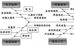
Common Surface Treatment Methods for PCBs
Long-term gradual changes will lead to significant changes. With the increasing call for environmental protection, the surface treatment processes for PCBs will definitely undergo major changes in the future. The Purpose of Surface Treatment The most fundamental purpose of surface treatment is to ensure good solderability or electrical performance. Due to the tendency of copper … Read more