
With the popularity of electronic products, there is a growing demand for digital systems to connect with the analog world to achieve changes, leading to an increasing need for Digital-to-Analog Converters (DACs). While designers are familiar with traditional voltage output DACs, many applications require current output DACs to provide precise, stable, high-resolution currents (tens or hundreds of milliamps) to control low-impedance resistors, inductors, and reactive loads.
Although these loads can be driven by voltage, using a current source or driver is more efficient and accurate for these sensors. However, current output DACs are not a simple “direct” replacement for voltage output DACs.
This article briefly explains why current output DACs are effective and often indispensable solutions. Additionally, it focuses on effective usage methods of current output DACs using two ICs from Analog Devices: the 6-channel 14-bit AD5770R and the 5-channel 16/12-bit LTC2662.
Comparison of DAC and ADC
Current Output DAC vs Voltage Output DAC
Some sensors and control loops require a DAC to precisely control current. These applications include speaker coils, solenoids, and motors; open-loop and closed-loop industrial systems, scientific systems, and optical systems related to control settings; basic resistive heaters or precision tunable lasers; automated test equipment (ATE) probe stimulation; precise current outputs for battery charging; and dimmable LEDs (Figure 1).
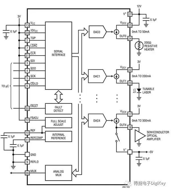 Figure 1: Current output DACs are suitable for applications such as optical amplifier nodes, controlling optical amplifiers, tunable lasers, and temperature-stabilized laser heaters, with this example using the LT2662 multi-channel DAC. (Image source: Analog Devices)
These are often low-impedance resistors, inductors, and magnetic loads. While these loads can also be driven by voltage, the relationship between voltage and end effect is more complex and often non-linear. Therefore, using a current source is more effective and precise for these types of sensors.
Designers are often less familiar with how to use current output DACs to generate precise current outputs. One way to convert a traditional voltage output DAC into a current output device is to add an operational amplifier configured as a voltage-to-current (V/I) converter (Figure 2).
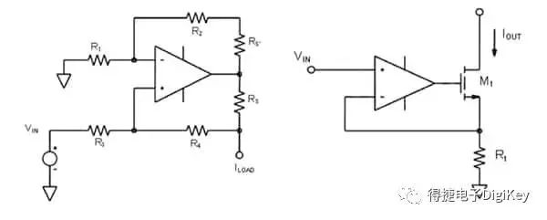 Figure 2: An operational amplifier (left) or an operational amplifier with a MOSFET boost output (right) can convert a voltage source into a current source, but may be relatively difficult to implement compared to designs actually using current output DACs, or technically less satisfactory. (Image source: Analog Devices)
However, this method requires adding more active and passive components to the bill of materials (BOM) and printed circuit board, and the operational amplifier must have good sourcing/sinking current capability; otherwise, a MOSFET boost must be used. Additionally, due to the addition of more active components with independent specifications and passive components, the error budget of the digital input/current output transfer function becomes increasingly challenging across the entire output range and temperature range.
Addressing Issues
Whether it is a current output or voltage output device, DACs are primarily defined by resolution and update speed. Current output DACs are typically not used for signal processing/analysis or waveform generation. Furthermore, due to their electromechanical characteristics or thermal characteristics, typical load changes for current output DACs are usually relatively slow. Therefore, the resolution range for these DACs is between 12 bits and 16 bits, with update rates of tens or hundreds of thousands of samples per second.
However, when selecting or using current output DACs, users must be aware of and address some key issues that may not exist when using voltage output DACs:
-
Compliance Voltage and Headroom
-
Current Driving Range and Resolution (Enhancing Both Characteristics)
-
Power-On Reset (POR) and Output Glitch Transients
-
DAC Data and Output Integrity; Accuracy
-
Thermal Management
Below, we will delve into these design issues using the AD5770R and LTC2662 as examples.
1. Compliance Voltage and Headroom
In addition to the conventional linearity and accuracy specifications of DACs, current output DACs have two parameters that voltage output DACs do not possess: compliance voltage and headroom.
Compliance voltage is the maximum voltage that can be achieved when the current source output is required to provide current—a fundamental yet critical scenario. As long as the voltage across the load is within the design limits, the current source can drive the load; to output the required current from the current source, the required voltage must be applied across the load. The current source can adjust the output voltage to provide the required current to the load.
For example, driving a 1kΩ load with a current of 10mA requires at least 10V of compliance voltage. If this voltage drop exceeds the compliance voltage, the DAC will not be able to output that current. Conversely, if the load current exceeds the rated current of the voltage source, the voltage source will also be unable to provide the nominal power supply voltage.
Assuming the DAC (or any current source) drives 10 series-connected LEDs, each with a voltage drop of 1.5V, at a current of 20mA. If the current source cannot output 20mA at a DC voltage of 15V (plus some margin), it will not be able to output that current, even if it can easily achieve it at a lower voltage. For current output DACs, the closer the compliance voltage is to the DAC output stage power supply rail, the larger the DAC output range.
Why discuss compliance voltage? Although it is a fundamental characteristic of current sources (according to V=IR), some less experienced engineers who have only dealt with voltage sources often overlook this issue. After all, if engineers hear that a 12V power supply is needed, the first question is often “What is the current?” However, for current sources, the corresponding question should be “What is the compliance voltage?” which is often overlooked.
The compliance voltage of a current output DAC is not limited by the DAC’s own power supply rail. For instance, each channel of the multi-channel LTC2662 has independent power pins, allowing each channel’s compliance voltage to match the load requirements while maximizing total dissipated power.
Moreover, current output DACs also have a headroom limitation, which is the minimum voltage drop required by the DAC to maintain output regulation. Headroom is a function of load current; the smaller the headroom, the wider the operating range of the DAC. The current output of the 5-channel LTC2662 has high compliance voltage, ensuring a 1V headroom when outputting 200mA of current (Figure 3).
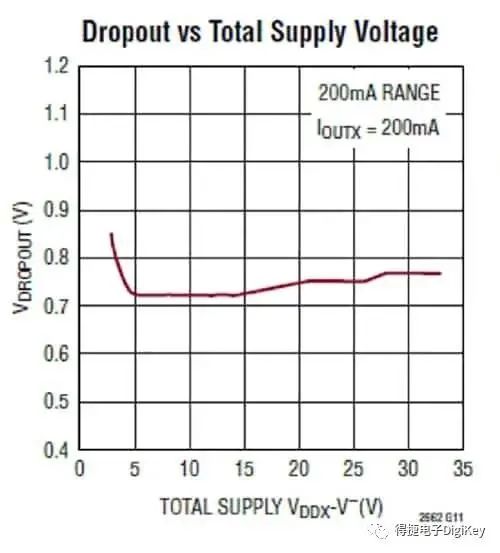 Figure 3: The headroom of the LTC2662 is below 1V across the entire current output range, ensuring sufficient operating margin for all output current values. (Image source: Analog Devices)
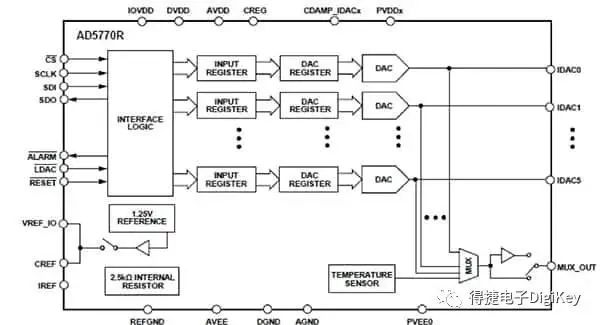 Figure 4: Analog Devices’ AD5770R is a 6-channel 14-bit current output DAC with an on-chip reference voltage source and serial peripheral interface (SPI), among many other features and functions. (Image source: Analog Devices)
The channel configuration is as follows:
Channel 0: 0 mA to 300 mA, -60 mA to +300 mA, -60mA to 0 mA
Channel 1: 0 mA to 140 mA, 0 mA to 250 mA
Channel 2: 0 mA to 55 mA, 0 mA to 150 mA
Channels 3, 4, 5: 0 mA to 45 mA, 0 mA to 100 mA
-
Provides a convenient solution for increasing maximum driving current
-
Greater output range but the same resolution, hence smaller step size but more precise output current
-
Allows for combined outputs to achieve low/high resolution
Regarding the first point, these current sources can simply be paralleled. For example, the channel 1 (250mA) and channel 2 (150mA) of the AD5770R can be summed to provide a total drive of 400mA (Figure 5). Of course, designers should not overlook the following warnings: the compliance voltage must be within the range specified in the datasheet; the output voltage must remain within the maximum absolute rating specified in the datasheet.
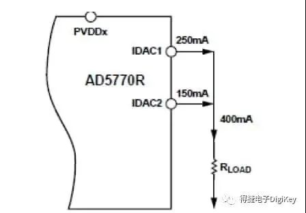 Figure 5: The outputs of these DACs can be combined in parallel, easily providing large currents; in this figure, a 250mA current source and a 150mA current source can provide a total of 400mA of fully controllable current. (Image source: Analog Devices)
Similarly, the 5-channel LTC2662 has eight current ranges, with each channel programmable, with full-scale outputs of 300mA, 20mA, 100mA, 50mA, 25mA, 12.5mA, 6.25mA, and 3.125mA; these currents can be combined to achieve a maximum output current of 1.5A.
With the low-resolution and high-resolution settings (the third point mentioned above), parallel outputs can also provide a straightforward method to enhance the overall resolution of the required nominal output value. By paralleling a wide-range output with a narrow-range output, the former can be set for low resolution while the latter is set for high resolution, thus providing a resolution that can exceed the 12/16-bit ratings of each channel (but must occupy 2 of the 5 channels).
3. Power-On Reset (POR) and Output Glitch Transients
In many applications, the DAC output at power-on (known as Power-On Reset, POR) can be a challenge because the processor (and its software) may not immediately initialize the DAC. While initializing the DAC in the processor code has the highest priority, the startup time of processors with multiple DC power rails may be longer than that of a simple DAC.
The time difference between the processor and DAC startup can lead to unacceptable DAC outputs—such as in cases where the DAC controls active components. Therefore, understanding the state of the DAC channels during POR becomes particularly important. For the above reasons, the output of the LTC2662 resets to a high-impedance state at power-on, ensuring consistent and repeatable system initialization. The AD5770R features an asynchronous reset pin that can be driven by a hardware timer or reset lock; setting the pin low for more than 10ns will reset all registers to their default values.
In addition, glitches during output transitions can also be problematic. Whenever the DAC loads new code mode data bits, due to clock offsets between the two codes, the DAC may produce erroneous outputs during the transition from old to new codes; like POR, this can also be unacceptable. To avoid this situation, the LT2662 and AD5770 will double-buffer the data being loaded into the DAC. All data bits for single or multiple channels can be written to the corresponding input registers without affecting the DAC output. A single command to the device to “load DAC” will send the contents of the input registers to the DAC registers, updating the DAC output without glitches.
4. DAC Data and Output Integrity; Accuracy
Most applications for these DACs involve active and mechanical components, making it necessary to verify the performance of the DAC. This requires attention to the digital input of the DAC and the actual current output values.
For integrity issues, advanced DACs like the AD5770R and LTC2662 can provide various solutions: data readback, data integrity confirmation based on internal cyclic redundancy checks (CRC), and indirect output current measurement. The first two are used for confirming data sent to and stored in the DAC; the third is used for monitoring current produced by the DAC.
Since software must initiate the readback and compare its value with the original sent value, basic data readback requires processor operation and incurs CPU load. However, the built-in CRC function of the AD5770R does not impose any burden. The AD5770R performs periodic background CRC operations on the on-chip data registers, ensuring that memory bits are not corrupted. If data errors are detected, an alarm flag is set in the status register.
The final test to ensure reliable DAC performance is to measure the output current and compliance voltage values. Both the AD5770R and LTC2662 have diagnostic features that allow users to monitor these parameters through multiplexed voltages. Users can select the corresponding voltages from the multiplexer output for measurement using an external ADC. For the AD5770R, current monitoring can be accurate within 10% of the full-scale output range, sufficient to determine gross errors and faults. If designers require higher output monitoring accuracy, they can calibrate the readings.
The absolute accuracy of the DAC output largely depends on the performance of the reference voltage source and some internal precision resistors. The AD5770R includes a 1.25V reference voltage source with a maximum temperature coefficient of 15 ppm/°C; the LTC2662’s 1.25V reference voltage source has a temperature coefficient of 10ppm/°C. With the performance of these precision reference voltage sources in DACs, designers can more easily achieve system accuracy goals, as these reference voltage sources can also be used externally (with additional buffering).
Specifications of 10ppm/°C and 15ppm/°C for internal reference voltage sources may be sufficient for most cases. However, considering the wide operating temperature ranges of these DACs (AD5770R: -40°C to +105°C, LTC2662: -40°C to 125°C), the reference voltage source may drift too much due to temperature in some cases.
Both DACs provide solutions: external reference voltage sources can be used, with internal buffers provided for those reference sources. If a lower temperature coefficient is needed, low-drift reference voltage sources like LTC6655 (temperature coefficient of 2ppm/°C) can be chosen. Using such high-performance external reference voltage sources is not easy: careful attention must be paid to PCB layout, mechanical stress, production soldering temperature profiles, and other details that can easily damage specific performance.
5. Thermal Management
It is essential to remember that these DACs supply power to loads in the form of controlled currents. Therefore, IC dissipation and self-heating are issues that must be analyzed to ensure they do not exceed the maximum allowable temperature of the internal chip. In most cases, heat dissipation needs to be done through the printed circuit board, using IC solder balls as thermal conduits.
During thermal analysis, the peak current, average current, and associated dissipation for each channel should be analyzed first. Then, thermal modeling should be performed on the path from the IC to the circuit board and the thermal capability of the circuit board (for example, layer count, available copper area, and other components using the same thermal area). The AD5770R (powered by a single supply from 2.9V to 5.5V) provides calculation examples in the datasheet showing the power dissipation at a specific ambient temperature when all outputs are providing specified currents. Designers can use this as a guide and conduct preliminary analysis for specific situations.
To avoid unnecessary dissipation, each output channel of the LTC2662 has independent power pins. Each channel can be powered by independent supplies from 2.85V to 33V, allowing for adjustment of dissipated power and compliance current margin for various loads.
Comprehensive Applications
Although the concept is simple, multi-channel current output DACs like the AD5770R and LTC2662 have numerous registers for controlling range settings, data loading, readback, and flagging basic functions. In addition to the physical connections required for the SPI bus and DAC output, there are many other options.
For these reasons, using evaluation boards (such as the DC2629A-A for the LTC2662 and related software) can save time and minimize hassle while simplifying the performance evaluation of the DAC in real-world applications (Figure 6).
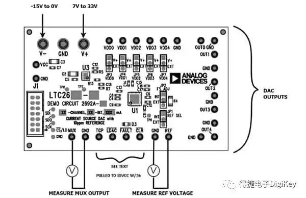 Figure 6: Demonstration circuits and evaluation boards (e.g., the DC2629A-A for the LTC2662 current source DAC) simplify connections, allowing the many functions and features of multi-channel current output DACs to be used at any time. (Image source: Analog Devices)
The evaluation board is designed for the 16-bit LTC2662, simplifying connections to the DAC and allowing evaluation of optional features such as the use of external reference voltage sources. The demonstration circuit connects the user’s computer via a USB cable.
The accompanying software GUI control panel can be used to operate the DAC, easily utilizing all features and functions (Figure 7).
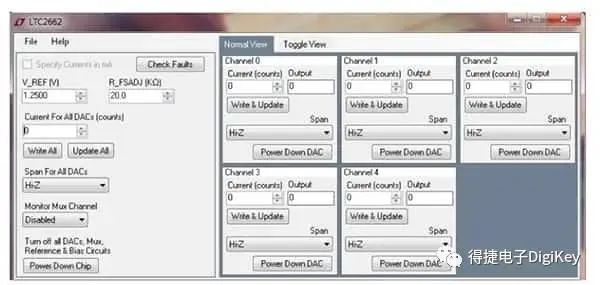 Figure 7: By connecting to a computer via USB, the evaluation software and GUI can be used to set and execute most registers and options of the LTC2662 DAC—this is an indispensable process in design work. (Image source: Analog Devices)
Conclusion
Although current output DACs are not as well-known as voltage output DACs, they are indispensable devices for many practical applications and loads. These DACs, especially multi-channel devices like Analog Devices’ AD5770R and LTC2662 with high output currents, offer numerous functions and user settings that enable designers to optimize compatibility and performance in their target applications. Users who understand these DACs and their characteristics will surely benefit from their functionalities and features.
This article is reproduced from the WeChat public account “DigiKey Electronics”
Editor: Amy Guan