The third-generation semiconductors, known as the “cornerstone of future electronics industry,” refer to wide bandgap semiconductor materials represented by silicon carbide (SiC) and gallium nitride (GaN). Due to their performance advantages, they have broad application prospects in fields such as semiconductor lighting, new energy vehicles, next-generation mobile communications, renewable energy grid integration, and high-speed rail transportation.
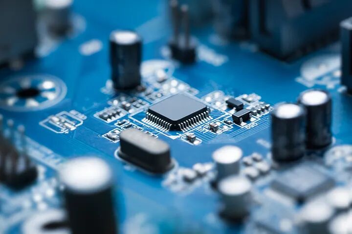 Image Source: Visual China
As international industrial competition intensifies, the third-generation semiconductor industry has become a battleground for various countries. The “Guiding Opinions on Accelerating the Cultivation and Development of Future Industries” issued by our province clearly states that priority should be given to the development of ten growth-oriented future industries, with the third-generation semiconductor industry placed at the forefront. Jiangsu ranks among the top in the country in terms of industrial development level in this field, with the highest number of representative enterprises nationwide, and key materials and production equipment possessing international leading advantages, accelerating the creation of a domestic leading and internationally advanced third-generation semiconductor industry hub.
In this competition concerning the high ground of future industries, what allows Jiangsu to stand out? How will it continue to lead?
Dual Core Shines, Innovative Achievements Emerge
In the semiconductor industry, there is a saying: “China’s semiconductors look to Jiangsu, and Jiangsu’s semiconductors look to Wuxi.”
How strong is the semiconductor industry in Wuxi? Semiconductors are the physical foundation of integrated circuits, and integrated circuits are the main application direction of semiconductor technology. According to Liu Feng, Deputy General Manager of the Sales Center of Wuxi Yiweng Microelectronics Technology Co., Ltd.: “To produce an 8-inch integrated circuit wafer, all processes such as photolithography, etching, testing, and packaging can be completed in Wuxi without leaving the city.”
In June, Yiweng Technology’s self-developed 12-inch CCP dielectric layer etching machine SPC12D was officially delivered to Chengdu BYD Semiconductor; in July, the first 12-inch CVD chemical vapor deposition equipment SPV12D was also delivered to BYD’s production line. “In just one month, our two core devices were successively delivered, marking that Yiweng Technology’s domestic equipment has successfully entered the core process circle of 12-inch semiconductors, equipping automotive-grade chip manufacturing with a ‘Chinese core’ engine,” Liu Feng remarked. “The equipment we produce has been booked by BYD, the Chinese Academy of Sciences, Hefei Jinghe, etc., and the order backlog has reached early 2026.”
On the list of “Pilot Projects for the Aggregated Development of Future Industries” announced at the 2024 Future Industry Innovation Development Exchange Conference, Wuxi’s Xinwu District and Nanjing’s Jiangning District were successfully selected as pilot areas in the third-generation semiconductor field.
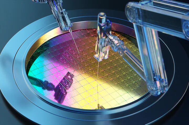 Image Source: Visual China
Turning our attention to Nanjing, we enter the National Third-Generation Semiconductor Technology Innovation Center (Nanjing) platform. In the ultra-clean workshop, researchers sit in front of computers controlling precision instruments that operate automatically; in the production workshop, automated testing platforms are testing a completed 6-inch SiC wafer, with testing probes moving at high speed between chips, finer than a needle… Scenes rich in “new” elements are everywhere.
Song Xiaofeng from the National Third-Generation Semiconductor Technology Innovation Center (Nanjing) platform introduced that the Nanjing platform serves as a “central hub” in the entire industrial ecosystem, driving technological advancements in manufacturing equipment and substrate epitaxial materials upstream, while outputting domestically produced autonomous chips downstream, meeting application demands and promoting key breakthroughs and overall leaps in the industry across the province and even the country.
Since its establishment, the innovation center has continuously achieved breakthroughs. Song Xiaofeng stated that the innovation center has built a shared platform for third-generation semiconductors, enhancing regional innovation capabilities, and serving innovation entities such as universities, enterprises, and research institutions in response to application demands in new energy vehicles, smart grids, rail transportation, and 5G communications. At the same time, it has focused on developing new tracks for electric drive chips for new energy vehicles and ultra-high voltage chips for power grids, successfully developing the first domestic 10kV SiC MOSFET and 20kV SiC IGBT, and demonstrating applications in the world’s first 35kV all-SiC substation and other projects.
Powerful Engine, Leading Advantages Steadily Expanding
The vigorous development of the third-generation semiconductor industries in Wuxi and Nanjing is just a microcosm of the province’s industrial development. Xuzhou Tianke Heda’s products cover conductive and semi-insulating silicon carbide wafers ranging from 2 to 8 inches, with technology levels leading domestically, while Zhuoyuan Semiconductor possesses the most advanced first large-diameter diamond substrate R&D line in the country… Jiangsu has a solid foundation and obvious advantages in this field, with industrial scale and technological innovation levels consistently ranking in the top tier nationwide.
Xu Xinyin from the Provincial Strategic and Development Research Center introduced that our province has initially formed a relatively complete third-generation semiconductor industrial chain centered on “equipment and auxiliary materials – substrates and epitaxy – device manufacturing,” supported by downstream applications, with an estimated operating income of about 5 billion yuan in 2024, establishing a development pattern with Nanjing, Suzhou, and Wuxi as the industrial core areas, and Nantong, Yangzhou, and Xuzhou accelerating collaborative development.
How does Jiangsu achieve this? Behind this success is the continuous increase in innovative talent. Academician Zheng Youchun from Nanjing University and other experts have achieved several internationally leading results in fields such as III-nitride heterostructures, and five universities, including Nanjing University and Southeast University, have established integrated circuit colleges to provide solid talent support for industrial development.
Behind this success is the ongoing efforts of research platforms. Relying on high-level R&D platforms such as the Semiconductor Display Materials and Chips Key Laboratory of the Suzhou Institute of Nano-Tech and Nano-Bionics, the 55th Research Institute of China Electronics Technology Group, and the Jiangsu Third-Generation Semiconductor Research Institute, our province has formed the capability to tackle key technologies across the entire industrial chain.
Li Lizhe, Senior Intellectual Property Manager at the Jiangsu Third-Generation Semiconductor Research Institute, introduced that the institute focuses on the autonomous controllability and high-quality development of the third-generation semiconductor industrial chain, leading the organization of key technology breakthroughs. “We have made breakthroughs in key core technologies such as 6-inch GaN materials, and achieved significant progress in homogeneous Micro-LED visible light communication technology, setting two world records, and completing the R&D of integrated chips for lighting, communication, and display, verified for the first time with independent intellectual property technology.”
A large number of major platforms support the leapfrog development of the industry and technology. Data shows that by June 2025, the number of invention patent applications in the third-generation semiconductor field in the province reached 6,593, with 2,448 granted, accounting for 16.02% and 14.02% of the national total, respectively, ranking among the top in the country.
Behind this success is the continuous improvement of the funding supply system in the third-generation semiconductor field. Wuxi has established a special fund of 5 billion yuan for third-generation semiconductors, focusing on supporting R&D investments in silicon carbide and gallium nitride device enterprises, promoting the process of domestic substitution. The Suzhou High-end Equipment Industry Special Mother Fund, funded by the provincial strategic emerging industry mother fund, will be listed on the main board of the Hong Kong Stock Exchange in 2024, becoming the first stock in Hong Kong’s “third-generation semiconductor” sector.
Gathering Strength to Break Through, Industrial Heights Rising
It is understood that in the development of first and second-generation semiconductor materials, China started later than other countries. However, in the field of third-generation semiconductor materials, domestic and foreign enterprises are at the same starting line. The vision of the Chinese industry is to “open the way and overtake” on the new track of third-generation semiconductors, and Jiangsu is accelerating its layout and continuous efforts.
Despite the good momentum of industry development, there are still challenges to overcome during the growth process.
Li Lizhe admitted that the development of the research institute has a strong demand for high-end talents who master core technologies of third-generation semiconductors, but domestic innovative talents in this field are often concentrated in universities and research institutions, and general enterprises lack the attraction for high-end talents. In addition, current policies have high requirements for flexible talent introduction, while top scientists often find it difficult to meet fixed time requirements, leading to limited depth of cooperation.
Enhancing the stability and security of the industrial chain and supply chain is also a key issue that urgently needs to be addressed. Song Xiaofeng introduced that the current international political and economic environment is complex, and technology embargoes and blockades have posed certain obstacles to the development of domestic third-generation semiconductors. In addition, the dependence on foreign core chips is still relatively high, with a significant portion of power devices for electric drives in new energy vehicles still relying on imports, facing issues such as high-end embargoes, low quality and high prices, and excessively long delivery times, urgently needing to accelerate the filling of industrial chain gaps.
The path to solutions is already underway, with various regions and institutions actively responding and accelerating exploration. Song Xiaofeng stated that the Nanjing platform will conduct frontier research on materials for the next generation of semiconductors. “It is recommended that relevant departments strengthen the innovation chain, increase R&D investment in silicon carbide devices, promote industrial agglomeration development, and strengthen upstream and downstream collaboration in the industrial chain to achieve win-win results. At the same time, it is essential to leverage the leading role of enterprises in innovation, accelerate the transformation of scientific and technological achievements, and support the construction of innovation platforms.”
“In the future, we will also improve the mechanism for cooperation between industry, academia, and research, accelerate the pace of technological innovation, and speed up the transformation of technological achievements to provide strong support for technological innovation in the third-generation semiconductor field in our province,” said a relevant official from the Provincial Development and Reform Commission. Jiangsu will focus on key directions, strengthen the hardware support for industrial development, expand the market space for industrial development, and gather strong momentum for industrial development, striving to create a domestic leading and internationally advanced third-generation semiconductor industry hub.
“After 3-5 years of high-quality development, the trend of collaborative development in Jiangsu Province in the field of third-generation semiconductors will become more apparent,” Li Lizhe expressed confidence in the development of Jiangsu’s third-generation semiconductor industry. “By building the National Third-Generation Semiconductor Technology Innovation Center to high standards, accelerating the promotion of the technological innovation network, incubation and cultivation chain, and improving the policy system, I believe our province will form a good innovation ecosystem. From the perspective of industry development, our province’s industrial scale will become more concentrated and expanded, and the application market will continue to expand.”
Source:Xinhua DailyEditor: Li Haihong
Reviewed by: Liu Tongjun