To ensure that the chips manufactured match the design functionality, the Design team must “sign off” to the foundry before the official tape-out: “As long as the process is within the following boundaries, my designed chip will definitely work.” This “guarantee” is known as the Sign-Off Corner. The Sign-Off Corner packages all uncertainties such as wafer manufacturing, voltage, temperature, interconnect variations, and on-chip fluctuations into a set of “extreme environments” to ensure that the chips produced match the simulation results as closely as possible. This reduces chip iterations and improves ROI.As an ATE test engineer, during the NPI CQS phase (Pre Release to Mass Production), we need to perform characterization testing on Corner Wafers to ensure stable yield during mass production (yield does not vary with the fabrication process parameters).Summary of IC Sign-off Corner related knowledge points are as follows: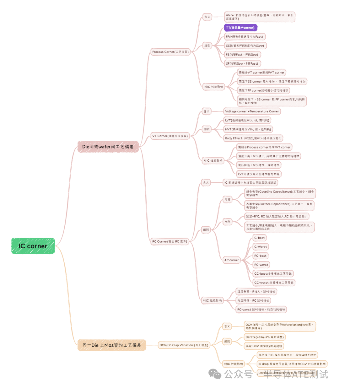
The “Four Families” of Sign-off Corner
Remember the formula in one sentence: Sign-off Corner = Process Corner + VT Corner + RC Corner + OCV
1. Process Corner (Transistor “Fast/Slow” Corners)
-
Source: Global deviations such as doping between wafers, between batches, oxide layer thickness, channel length, etc.
-
The Five Brothers:– TT: Typical NMOS + Typical PMOS (Nominal)– SS: Slow NMOS + Slow PMOS (Slowest)– FF: Fast NMOS + Fast PMOS (Fastest)– SF / FS: One slow and one fast, called “skew” corner, used to discover unusual paths.
-
Impact on Chips: Reference: idc-online.comAt high temperatures, SS corner increases delay (mobility decreases T^{-3/2}), possibly increasing by 20%+;
At low temperatures (<-50°C), delay increases due to threshold effects.
Voltage: High voltage FF reduces delay (saturation current increases), but increases dynamic power consumption (P=CV^2f).
Delay/Power Consumption:FF reduces delay, increases AI computation speed;SSincreases delay but reduces power consumption. Overall: affects timing margins, neglecting it leads to unstable performance.
2. VT Corner (Voltage-Temperature Corner)
-
V Corner: The foundry provides a voltage window, for example, 0.72 V ~ 0.88 V.– High voltage: Transistors are fast, setup is easy to pass, hold is difficult to pass;– Low voltage: Transistors are slow, setup is difficult to pass, hold is easy to pass.
-
T Corner: -40 °C ~ 125 °C.– Low temperature: mobility ↑, speed ↑;– High temperature: leakage ↑, speed ↓.
-
Impact on Chips:Reference: chu.berkeley.eduAt high temperatures, Vth decreases (approximately1mV per °C), reducing delay but increasing leakage power consumption (staticP = V I_off increases); at low temperatures,Vth increases, increasing delay.
Voltage: At low voltage,HVTincreases delay (switching is slow); at high voltage,LVTincreases power consumption.
-
Delay/Power Consumption:LVT reduces delay15%(for high-speed AI cores), but static power consumption increases;HVT is energy-saving but has tight delay. Body effects exacerbate the impact of voltage variations.
3. RC Corner (Interconnect “Routing” Corner)
| Corner Name | Meaning | Impact on Delay | Usage Scenario |
|---|---|---|---|
| Cbest (Cmin) | Minimum capacitance, maximum resistance | Shortest line is fastest | hold analysis |
| Cworst (Cmax) | Maximum capacitance, minimum resistance | Shortest line is slowest | setup analysis |
| RCbest (RCmin) | Minimum RC product | Longest line is fastest | hold analysis |
| RCworst (RCmax) | Maximum RC product | Longest line is slowest | setup analysis |
Advanced processes also need to account for the deviations of the upper and lower mask layers (DPT), resulting in combinations such as Cworst_CCworst, RCbest_CCbest, etc., ensuring that the coupling capacitance fluctuations caused by line spacing changes are also covered.
-
Impact on Chips: Reference: idc-online.com
At high temperatures, Vth decreases (approximately1mV per °C), reducing delay but increasing leakage power consumption (staticP = V I_off increases);
At low temperatures, Vtincreases, increasing delay.
At low voltage, HVT increases delay (switching is slow);
At high voltage, LVT increases power consumption. Delay/Power Consumption:
LVT reduces delay15%(for high-speed AI cores), but static power consumption increases;HVT is energy-saving but has tight delay. Body effects exacerbate the impact of voltage variations.
4. OCV (On-Chip Variation)
Even for the same chip, the transistors in the upper left corner and the lower right corner cannot be identical. OCV quantifies this local deviation using a “derate” coefficient:
-
Path Level: Data path slows down × derate, clock path speeds up × derate, forming the most pessimistic difference.
-
Advanced Mode: POCV (Parametric OCV) uses statistical σ values, with 3 σ covering 99.7% of chips.
-
Impact on Chips: Reference: Synopsys.com
Local hotspots (high temperatures) increase delay uncertainty; low temperatures exacerbate random variations.
Voltage:IR drop leads to local voltage changes, increasing OCV impact (e.g., delay ±10%).
Delay/Power Consumption:Derate increases timing margins (setup delay +%,hold -%), reducing over-design but if excessive, may increase power consumption. Advanced OCV improves slack by 32%, enhancing performance.
If all goes well, this should be the last article before the holiday~
Wishing everyone a happy National Day and Mid-Autumn Festival in advance!!!
If you want to join the group, please add the following WeChat, and the assistant will pull you into the group:
 Recommended Previous Articles~
I2C & I3C Notes — Part1FreyaW, WeChat Official Account: Semiconductor ATE Testing I2C & I3C Protocol Study Notes — Part1
SSN VS Typical ScanFreyaW, WeChat Official Account: Semiconductor ATE Testing SSN vs Traditional Scan
AIReflections on Restructuring the ATE IndustryFreyaW, WeChat Official Account: Semiconductor ATE Testing AI Restructuring the Technical Paradigm and Competitive Landscape of the ATE Industry
AECQ-100 BasicFreyaW, WeChat Official Account: Semiconductor ATE Testing Analysis of Automotive Semiconductor AECQ-100