Skip to content
Source: Semiconductor Industry Observation
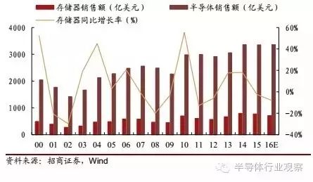
Memory, as an important component of semiconductor devices, accounts for as much as 20% of semiconductor products. As a significant type of semiconductor product, the global semiconductor market sales for memory reached $77.2 billion in 2015, representing a 23% share of the semiconductor product market, with total sales of $335.2 billion. As the world’s manufacturing base for electronic products, China has always been the largest demand market for memory products. According to research by CCID Consulting, the semiconductor memory market size in mainland China was 284.3 billion yuan (approximately $40 billion) in 2015.
Figure 1: Global Semiconductor Product Sales and Memory Sales
The Semiconductor Memory Market is Oligopolized by Samsung, Hynix, Micron, and Others
The semiconductor memory market is highly monopolized, especially the three mainstream products: DRAM, NAND Flash, and NOR Flash. The global market is mainly dominated by the top three companies, and the degree of monopoly has intensified in recent years. For instance, in Q1 2016, 93% of the DRAM market share was held by Samsung, Hynix, and Micron, while the NAND Flash market was almost entirely divided among Samsung, Hynix, Toshiba, SanDisk, Micron, and Intel.
(1) DRAM: Global market size is approximately $41 billion. Currently, the DRAM industry is dominated by Samsung, Hynix, and Micron, which together control over 95% of the market. In 2014, Samsung and Hynix excelled in advanced processes, with Samsung adopting a 20nm process at a gross margin of 42%, while SK Hynix primarily used a 25nm process with a gross margin of 40%. Micron’s process is still based on a 30nm process with a gross margin of about 24%, significantly lower than the other two. Hence, the monopoly pattern in the DRAM market is intensifying, especially for Samsung, which, by being the first to enter the 20nm mass production era, successfully sold many high-value-added products. Although the DRAM market slightly shrank in 2015, Samsung’s revenue instead grew, surpassing $20 billion, maintaining its position as the global market leader in DRAM for 24 consecutive years.
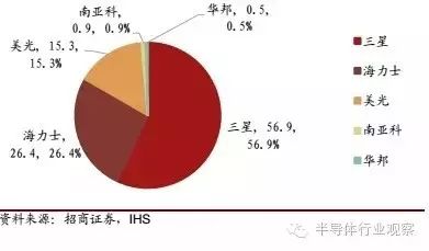
In the mobile DRAM market, Samsung and Hynix hold over 80% market share, showcasing overwhelming advantages.
Figure 2: Q1 2015 Mobile DRAM Major Suppliers Market Share
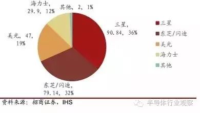
(2) NAND Flash: Global market size is approximately $30 billion. The monopoly situation for NAND is even more severe than that for DRAM. Samsung remains the industry leader, maintaining a market share of about 35% for several years. Toshiba and SanDisk have teamed up to secure the second position in the NAND sector, generally maintaining around 30% market share. Micron, with the help of Intel, ranks third. Hynix surpassed Micron in market share in 2011 and subsequently focused on DRAM, ranking fourth for three consecutive years from 2012 to 2014. These four companies monopolize the entire NAND market, with the degree of monopoly on the rise, increasing from 91.3% to 99.2% from 2011 to 2014.
Figure 3: 2014 NAND Major Suppliers Market Share
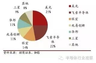
(3) NOR Flash: Global market size is approximately $3 billion. Compared to DRAM and NAND, the NOR market is much smaller and more fragmented. Currently, the market is mainly dominated by Micron, Cypress Semiconductor (acquired by Cypress), Winbond, Samsung, HwaCom, GigaDevice, and Etron Technology, with the top five being IDM models and the last two being fabless models. Among them, GigaDevice is the only company in China that holds a certain voice in the mainstream memory design industry, rapidly advancing in the NOR Flash field, rising from a 3.4% market share in 2012 to 11% in 2013, ranking fourth globally.
Figure 4: 2013 NOR Flash Major Suppliers Market Share
Comparison of Mainstream Semiconductor Memory Performance and Future Development Trends
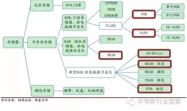
There are many types of semiconductor memory, each with different technical principles, advantages, and applicable fields. For example, SRAM (Static Random Access Memory) can use the two stable states of a flip-flop to represent information 0 and 1, meaning it can retain its stored data without needing to refresh the circuit, thus SRAM has very fast read and write speeds. However, it is very expensive and has high power consumption, used only in CPU level 1 and level 2 caches (Cache) where storage speed is crucial. Widely used products must balance performance and cost; from the market size perspective, the most mainstream memories today are DRAM, NAND Flash, and NOR Flash, which together account for about 95% of all semiconductor memory scale, especially the former two, which account for about 90% of the total scale.
Figure 5: Classification of Memory
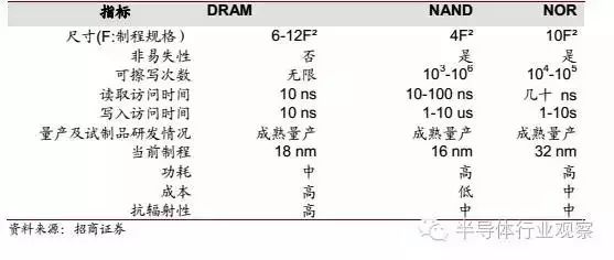
Table 1: Comparison of Traditional Memory Performance
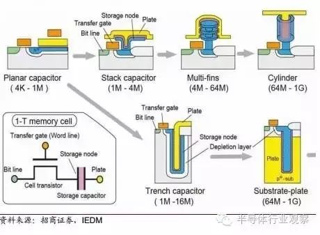
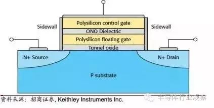
DRAM: Dynamic Random Access Memory, the term “dynamic” means that it needs to be refreshed periodically; otherwise, the internal data will disappear. This is because the basic unit of DRAM is a transistor and a capacitor, using the presence or absence of charge in the capacitor to represent binary information 0 and 1. The capacitor discharges quickly, so to prevent reading errors caused by capacitor leakage, DRAM must periodically charge its capacitors, making it slower than SRAM.
On the other hand, this simple storage mode allows DRAM to have a much higher integration than SRAM. A DRAM storage unit requires only one transistor and a small capacitor, while each SRAM unit requires four to six transistors and other components. Thus, DRAM has advantages in high density (large capacity) and price compared to SRAM. SRAM is mainly used in places with extremely high performance requirements (like CPU level 1 and level 2 caches), while DRAM is primarily used in computer memory modules and other fields.
Figure 6: DRAM Device Unit Diagram and Its Cross-Sectional Structure of Different Capacities
Future Development Trends of DRAM:
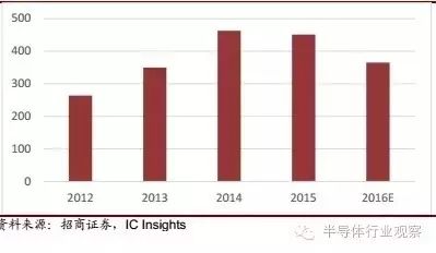
Overall scale decline due to PC drag: Overall, the mobile market has performed strongly in recent years, while PC sales have been eroded, compounded by the global GDP weakness. Institutions such as IC Insights and WSTS predict that the DRAM market scale will see a significant decline in 2016.
Figure 7: Global Market Size of DRAM
Rapid Growth of Mobile Terminal Memory: In addition to computer memory modules, mobile terminal memory is also a significant application area for DRAM. Thanks to the consumption trend of “mobility” in recent years, the mobile terminal DRAM market is growing rapidly. In 2009, mobile DRAM shipments accounted for only 5.1% of overall DRAM; by 2014, this proportion had surged to 36% and is still on the rise, expected to surpass 50% in 2015. In China, due to the large population and increasing smartphone penetration rate, the share of mobile DRAM reached 55% in 2014.
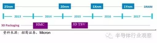
Flat microfabrication approaches physical limits; 3D packaging opens new paths: Each update of the DRAM process requires significant investment. For instance, transitioning from 30nm to 20nm requires a 30% increase in the number of photomasks and a doubling of non-photolithography process steps, with cleanroom area requirements increasing by over 80% due to the rising number of devices. Previously, these costs could be offset by the higher output and performance premiums from single wafers, but as the process continues to shrink, the gap between increased costs and revenues is gradually narrowing. Therefore, major manufacturers are beginning to explore Z-axis expansion capabilities. Samsung was the first to achieve 3D DRAM from a packaging perspective, using TSV packaging technology to stack multiple DRAM chips, significantly enhancing the capacity and performance of a single memory module.
Figure 8: Development Roadmap of DRAM
To better explain NAND Flash and NOR Flash, we first need to understand Flash technology.
Flash Memory: Also known as flash storage, it is a type of non-volatile memory. The storage unit of flash memory is a field-effect transistor, which is a three-terminal device controlled by voltage, consisting of a source, drain, gate, and substrate, with a silicon dioxide insulating layer between the gate and silicon substrate to protect the charge in the floating gate from leaking.
NAND’s erase and write operations are based on the tunneling effect, where current passes through the insulating layer between the floating gate and silicon substrate to charge (write data) or discharge (erase data) the floating gate. In contrast, NOR erases data based on the tunneling effect (current from the floating gate to the silicon substrate), but writes data using a hot electron injection method (current from the floating gate to the source).
Figure 9: Schematic Diagram of Flash Memory Structure
NAND Flash: NAND is currently the most significant product in flash memory, featuring non-volatility, high density, and low cost advantages. In NAND flash memory, data is stored in bits within Memory Cells, with one Cell storing one bit. These Cells are grouped in units of 8 or 16, forming bit lines, and these lines combine to form Pages, with NAND flash reading and writing data on a page basis and erasing data on a block basis. Although its write and erase speeds are approximately 3-4 orders of magnitude slower than DRAM, they are still three orders of magnitude faster than traditional mechanical hard drives, making NAND flash widely used in eMMC/EMCP, USB drives, SSDs, and other markets.
Figure 10: Global Market Size of NAND Flash
NAND Future Development Trends:
eMMC/eMCP Continues to Be Hot, Embedded Storage Market is Broad:
eMMC refers to embedded storage solutions, packaging MMC (Multimedia Card) interface, NAND, and main controller into a small BGA chip. System manufacturers only need to select the required capacity eMMC chip without worrying about NAND brand differences and compatibility issues, simplifying the new product launch process. eMCP integrates eMMC with LPDDR, further reducing module size and simplifying circuit connection design, primarily used in high-end smartphones. In 2014, eMMC/eMCP saw strong demand driven by mobile terminal growth, with NAND accounting for 25% and a compound annual growth rate of nearly 60%. eMMC 5.0 has become the standard configuration for domestic terminal smartphones. Additionally, the proportion of large-capacity eMCP modules is expected to increase, with Micron estimating that by 2018, the eMCP module of 32GB (eMMC) + 24GB (LPDDR) will exceed 40%.
SSD Prospects Are Promising:
Besides embedded products, SSD is also one of the main battlegrounds for NAND, with the demand for big data storage and high-speed transmission leading to rapid growth in demand for SSDs over 500GB in the server market. In the PC sector, HDDs are gradually unable to withstand the assault of SSDs. From 2010 to 2015, the performance, capacity, and cost of mainstream HDDs have hardly changed, while SSDs have closely followed Moore’s Law, making significant advancements in read/write speeds and capacity, with a sharp rise in cost-effectiveness.
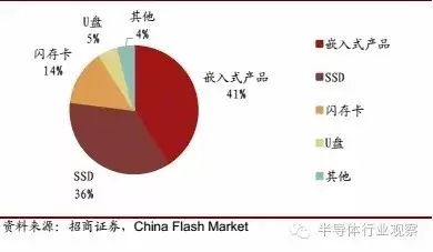
Figure 11: 2016 NAND Market Segmentation
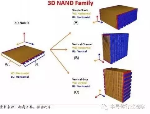
Technological Transition from 2D to 3D:
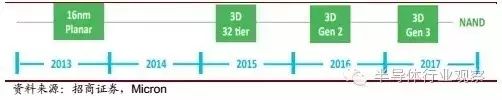
Currently, 16nm and 28nm are still the mainstream processes for NAND Flash. However, as the 2D NAND Flash process approaches its physical limits, the difficulty of flat microfabrication is increasing, particularly after entering the 16nm process. Continuing to use flat microfabrication has become more challenging and costly than 3D TSV technology. Major memory leaders successfully mass-produced 16nm NAND in 2013-2014, but due to economic considerations and future development prospects, these companies have not introduced smaller flat processes but have begun to shift focus to 3D NAND.
Figure 12: NAND 2D to 3D Development Roadmap
NOR Flash: The characteristic of NOR Flash is Execute In Place (XIP), meaning applications do not need to read the code into system RAM but can run directly in Flash memory. NOR has high transmission efficiency and much faster read speeds than NAND, providing high cost-effectiveness at small capacities of 1-4MB. However, its erasure is done in blocks of 64-128KB, with a write/erase operation taking about 5 seconds, while NAND devices can erase in blocks of 8-32KB, completing the same operation in a maximum of just 4ms. Thus, its low write and erase speeds significantly impact its performance. Additionally, the unit size of NOR is nearly twice that of NAND flash, making it less cost-effective, which has limited its application scope. Many markets that once belonged to NOR have gradually been taken over by other memory types, but NOR flash manufacturers have not remained idle; they are actively exploring markets such as automotive electronics and the Internet of Things. In recent years, the NOR flash market size has been continuously shrinking.
Figure 12: Global Market Size of NOR FLASH (in 100 million USD)
NOR Flash Future Development Trends:
Good Development Momentum in Automotive Electronics:
In the past, NOR Flash chips were primarily used in mobile phones to store code programs. However, since smart phones began adopting eMMC solutions, the proportion of NOR Flash used in mobile phones has significantly decreased, losing this major market to NAND. Currently, the most promising market for NOR Flash is automotive electronics, where NOR can be found in both the vehicle itself and peripheral entertainment and navigation systems. Honda and Toyota use Micron’s NOR Flash chips, while Nissan has partnered with Toshiba, which uses embedded NOR Flash chips with capacities mostly over 230Mb.
Industrial Control and Networking Fields Are Growing Rapidly:
Besides automotive electronics, NOR Flash chips are also widely used in industrial control and networking equipment, often utilizing high-capacity NOR Flash chips, with considerable growth potential in the future.
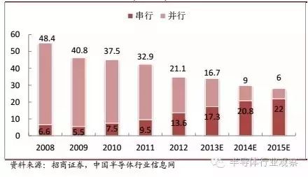
Parallel Weakening, Serial Growth:
Parallel NOR flash memory has gradually been replaced by serial NOR flash memory due to its many pins and low integration. In recent years, the global NOR Flash market size has not changed significantly, but internally, there is a trend of growth in serial NOR Flash and decline in parallel NOR Flash.
Challenges of Traditional Memory vs. Opportunities for New Memory
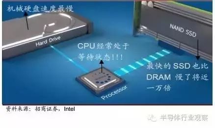
The main contradiction in the memory industry today is the growing performance demands of end products versus the lack of significant breakthroughs in technology. Specifically, the huge performance gap between internal and external storage has become the main bottleneck for improving electronic product performance. In recent years, SSDs have become the favorite among computer performance enthusiasts precisely because traditional mechanical hard drives often have transfer speeds below 200MB/s and seek times around 10ms; in contrast, NAND flash-based SSDs have transfer speeds ranging from hundreds of MB/s to several GB/s and seek times of about 0.1ms, providing a dramatic speed increase that feels like a computer upgrade. However, even the top SSDs have latencies in the microsecond range, nearly 10,000 times slower than DRAM, with transfer speeds an order of magnitude slower, preventing DRAM from fully realizing its performance.
Figure 13: Memory Performance Bottleneck
1. The Three Major Storage Technologies Each Have Shortcomings
In addition to the performance gap between internal and external storage, the three major semiconductor memories also have various shortcomings:
DRAM: Volatile data, small capacity. Although DRAM has excellent performance—nanosecond-level latency and bandwidth in the tens of GB/s, akin to being “immortal”—it is a volatile memory, meaning data is lost upon power failure. Moreover, its cost is higher than flash memory, and its capacity is relatively small. Although there is still some distance before flat microfabrication approaches its physical limits, continuing to reduce dimensions in two dimensions after 18/16nm no longer has advantages in terms of cost and performance.
NAND: Long latency, short lifespan, flat microfabrication has reached its limits. NAND flash has advantages such as low cost (relative to DRAM), low power consumption, non-volatility, and small size, but because it requires high voltages to write data, the process can cause irreversible damage to the oxide layer, leading to a limited number of read/write cycles. The best-performing SLC NAND has about 100,000 read/write cycles, while lower-performing MLC and TLC have lifespans in the thousands. The situation regarding process miniaturization is similar to DRAM; after entering the 16nm process, the cost of 2D NAND has risen sharply, and continuing to use flat microfabrication has become more challenging and costly than 3D TSV technology. Additionally, as the insulating layer is thinned, electrons may tunnel under insufficient voltage, affecting chip reliability.
NOR: Small capacity, slow write and erase speeds. The advantage of NOR Flash is that applications can run directly in Flash memory without reading code into system RAM, resulting in high transmission efficiency and fast read speeds, with high cost-effectiveness at small capacities of 1-4MB, primarily used for program storage. However, the device structure requires that all bits be written to 0 before erasing, which results in low erase speeds, and since data must be erased before writing, this also affects NOR’s write speed.
In summary, the existing memory issues mainly involve the mismatch of performance between internal and external storage, the non-volatility of memory, and the challenges of miniaturization for external storage. Therefore, many companies and research institutions are urgently seeking to develop new types of memory that can simultaneously possess the high speed and long lifespan of DRAM and the low cost and non-volatility of FLASH.
2. Classification and Advantages of New Memory Types
As traditional mainstream memories face challenges, new memory technologies are worth attention. Innovations in memory mainly involve two approaches: transitioning from 2D to 3D structures and adopting new memory device structures or materials. In this section, we will compare and analyze the most significant new memory types from the perspectives of device structure, functional characteristics, and research progress. 3D XPoint technology is the most revolutionary hot technology, so it will be analyzed separately in the next section.
Currently, the mainstream processes for NAND flash memory are 28nm/16nm. As processes enter the 1x nm generation, the crosstalk effect between increasingly closely spaced storage cells and the electronic breakdown effect caused by thinner gate oxide layers have begun to impact the reliability and performance of NAND. Furthermore, after entering the 2x nm generation, the difficulty of flat microfabrication has increased, leading to a decline in the cost advantages brought by miniaturization, especially after the 16nm process, where continuing to use 2D miniaturization has become more challenging and costly than 3D techniques such as silicon through vias.
Figure 14: Comparison of 2D NAND and 3D NAND
In other words, whether considering performance or economic factors, continuing flat miniaturization is not a good approach. Therefore, leading NAND companies such as Samsung, Hynix, Toshiba, and Micron are actively developing 3D NAND technology. IC Insight predicts that driven by SSDs and smartphones, the shipment volume of 3D NAND will increase at a compound annual growth rate of 200% starting in 2015 (while 2D will decline at an annual rate of 17.1%), expected to reach 70% of total NAND volume by 2020.
1) Achieving large capacity easily under relaxed processes: Transitioning from 2D NAND to 3D NAND is like moving from a single-story house to a skyscraper, thus higher capacity per unit area. Currently, a 32-layer 3D NAND has a capacity of 128Gb, comparable to mainstream 2D 1y/1znm NAND, while a 48-layer 3D NAND can reach 256Gb, with the power of 3D beginning to show once the number of layers reaches 48. Samsung predicts that 100-layer 3D NAND will reach 1TB capacity.
2) Higher performance and lower power consumption: Thanks to the three-dimensional stacking model, 3D NAND can maintain high storage density at larger storage unit sizes, allowing larger storage units to receive charge signals more fully, with thicker gate oxides that are less prone to breakdown. Moreover, larger capacity NANDs require fewer retries during read/write operations, thus overall power consumption will also be lower.
Comparison of Mainstream Technologies:
Due to the significant differences in the processes, the progress of 3D NAND development has not been smooth sailing. Currently, the R&D of 3D NAND can generally be divided into three camps: Samsung, Hynix, and Toshiba, each with similar technologies and proprietary techniques. The commonality is that all three use gate-all-around (GAA) technology, enhancing the control capability of the gate over the conductive channel and reducing leakage current. The main differences are threefold:
Samsung and Hynix have introduced a Charge Trap Layer (CTL) in their 3D NAND products, storing charge in a high-k dielectric material layer (SiN). In contrast, traditional 2D NAND stores charge in conductive polysilicon floating gates. Due to the special structure of silicon nitride, charge tends to accumulate around its lattice, theoretically preserving these charges without consumption, thus improving lifespan. Meanwhile, Intel/Micron still uses traditional floating gates, reasoning that this technology has been thoroughly tested and is mature in 2D NAND.
Toshiba/SanDisk and Western Digital are in a cooperative relationship regarding 3D NAND (Western Digital acquired SanDisk in 2016), employing a technology called BiCS (Bit Cost Scaling), allowing all memory cells in the 3D stack to be produced simultaneously using the same wafer deposition steps. Also, each bit line in the stacked memory cells only requires one bit line, thereby reducing costs as NAND scale increases, claiming to have the lowest core area and cost among all 3D NAND flash memory. In 2015, Toshiba/SanDisk launched the second-generation 3D NAND Flash (BiCS2), which stacked 48 word line layers in a 2bit/cell (16GB) chip, with a capacity of 16GB, using a “U” type NAND string structure to improve array density.
Toshiba and Hynix use self-aligned polysilicon gates, while Samsung deposits metal gates through a damascene process.
Similar to NAND Flash technology, DRAM’s flat miniaturization is also gradually approaching its limits and expanding vertically. After 18/16nm, due to the inability to continue reducing film thickness and the unsuitability of high-k materials and electrodes, continuing to reduce dimensions in two dimensions no longer has advantages in terms of cost and performance. Unlike the 3D technology roadmap for NAND, the 3D technology for DRAM is reflected at the chip level rather than the transistor level, meaning that its 3D refers to 3D packaging—stacking multiple chips together using TSV technology. As the demand for DRAM capacity and performance increases, the proportion of 3D DRAM is expected to rise in the future.
a) Achieving high-density capacity under relaxed dimensions: Similar to 3D NAND, the ability to expand in the Z direction reduces the requirements for flat miniaturization, allowing for significant increases in single memory module capacity at larger processes.
b) Reduced parasitic resistance and capacitance, lower latency crosstalk: After switching to 3D packaging, many connections between chips changed from mixed copper wires on a horizontal plane to vertical vias, significantly reducing the length of interconnections, greatly improving latency and crosstalk between back-end lines, which significantly helps enhance chip performance.
3) PCRAM (Phase Change Memory)
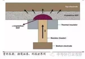
PCRAM (Phase Change RAM): Phase Change Random Access Memory utilizes the differences in conductivity between the crystalline and amorphous states of materials to store information, mainly divided into SET and RESET steps. When the material is in the amorphous state, raising the temperature above the recrystallization temperature but below the melting point, then slowly cooling (this process is the key factor limiting PCM speed), the material will transition to a crystalline state (this step is called SET), at which point the material has long-distance atomic energy levels and a higher density of free electrons, resulting in low resistivity. When the material is in the crystalline state, raising the temperature slightly above the melting point and then quenching rapidly will convert the material back to the amorphous state (this step is called RESET), at which point the material has short-range atomic energy levels and a lower density of free electrons, resulting in high resistivity. The resistivity difference between the crystalline and amorphous states can vary by several orders of magnitude, providing high noise tolerance sufficient to distinguish between “0” and “1” states. Currently, the most commonly used phase change materials are chalcogenides (represented by Intel) and synthetic materials containing germanium, antimony, and tellurium (GST), such as Ge2Sb2Te5 (represented by STMicroelectronics).
Figure 15: Structure Diagram of PCM
a) Low latency, balanced read/write times: Compared to NAND flash, PCM does not need to erase previous codes or data before writing updates, giving it a speed advantage over NAND and more balanced read/write times.
b) Long lifespan: PCM read/write operations are non-destructive, significantly enhancing its write endurance, making PCM a more reliable alternative to traditional mechanical hard drives.
c) Low power consumption: PCM has no mechanical moving parts and does not require refresh current to maintain codes or data, resulting in lower power consumption than HDDs, NAND, and DRAM.
d) High density: Some PCM designs utilize non-transistor structures, enabling high-density storage.
e) Good radiation resistance: PCM storage technology and materials are not affected by charged particle states, giving it strong resistance to space radiation, meeting the needs of defense and aerospace.
Challenges in PCM Development:
A) Balancing device power consumption and speed: To reduce device power consumption, the thermal conductivity of phase change materials should be minimized to improve thermal utilization; however, excessively low thermal conductivity can lead to high adiabatic constants in phase change units, hindering quick cooling after RESET, impacting device speed.
B) Thermal crosstalk issues at high density: When a phase change material in a device unit is in a high-temperature molten state, thermal diffusion may cause adjacent device units to also undergo phase changes, leading to storage errors.
C) Crosstalk current affecting data stability: Currently, diodes are a major choice for switching devices in high-density PCM. However, their manufacturing process can lead to parasitic transistors forming between adjacent diodes on the same word line, and the crosstalk current from these parasitic transistors can affect data stability.
D) Materials need to have both high crystallization temperatures and low melting points: The data retention time is related to the thermal stability of the amorphous state, meaning PCM materials need much higher crystallization temperatures while not having excessively high melting points to reduce power consumption.
E) Volume changes during phase transitions affecting device reliability: When materials transition between amorphous and crystalline states, their volume changes, potentially leading to delamination between phase change materials and their contact electrode materials, causing device failure.
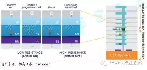
4) RRAM (Resistive Random Access Memory)
RRAM (Resistive Random Access Memory): A typical RRAM consists of two metal electrodes sandwiching a thin dielectric layer, which serves as the ionic transport and storage medium. The choice of materials can lead to significant differences in operational mechanisms, but the essence is that external stimuli (such as voltage) cause ionic movement and local structural changes in the storage medium, resulting in resistance changes, which are used to store data. The most accepted mechanism for RRAM is the conductive filament theory, where filament conduction devices do not depend on the area of the device, indicating significant miniaturization potential. RRAM materials are mainly metal oxides, with sulfides and organic materials also receiving attention.
Figure 16: RRAM Device Unit and Storage Principle
High speed: RRAM write and erase speeds are determined by the pulse width of resistance changes, generally less than 100ns.
Durability: RRAM read/write operations differ from NAND, employing a reversible non-destructive mode, greatly enhancing its lifespan.
Multi-bit storage capability: Some RRAM materials can have multiple resistance states, allowing individual storage units to store multiple bits of data, thus increasing storage density.
Filament resistance expansion difficulty: Most RRAMs are filament-based, requiring programming to track each filament change. Therefore, expanding this technology is challenging, and speeds are not ideal. Moreover, filament structures elevate current density, impacting performance and reliability.
Crosstalk between adjacent units and the difficulty of balancing device miniaturization: The RRAM storage matrix can be divided into passive and active matrices. In passive matrices, storage units consist of a resistive switching element connected to a nonlinear element (usually a diode), which helps ensure proper voltage division across the resistive switching element, preventing data loss when the storage unit is in a low-resistance state. This method is straightforward and favorable for miniaturization, but passive matrices inevitably lead to interference between adjacent units. Active units control the read/write and erase operations of resistive switching devices using transistors, effectively isolating interference between adjacent units, but their design is more complex and has poorer miniaturization capabilities.
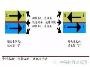
MRAM (Magnetic RAM): Magnetic Random Access Memory stores data using magnetic polarization rather than electrical charge. The storage unit of MRAM consists of a free magnetic layer, a tunnel barrier layer, and a fixed magnetic layer. The direction of polarization in the free magnetic layer can change, while the direction of the fixed layer’s magnetic field remains unchanged. When the magnetic fields of the free and fixed layers are parallel, the storage unit shows low resistance; otherwise, it shows high resistance. By detecting the resistance of the storage unit, it can determine whether the stored data is 0 or 1.
Figure 17: MRAM Storage Unit
Non-volatile: The magnetism of ferromagnets does not disappear when power is lost, giving MRAM its non-volatility.
Unlimited read/write cycles: The magnetism of ferromagnets not only does not disappear when power is lost but can be considered virtually everlasting, allowing MRAM to be rewritten infinitely like DRAM.
Fast write speeds, low power consumption: In currently available experimental samples, MRAM’s write times can be as low as 2.3ns, and it consumes very little power, allowing for instant on/off capabilities and extending the battery life of portable devices.
High integration with logic chips: MRAM units can be easily embedded into logic circuit chips, requiring only a few additional steps in the backend metallization process. Additionally, MRAM units can be entirely fabricated within the chip’s metal layers, even allowing for 2-3 layers of units to be stacked, giving it potential for constructing large-scale memory arrays on logic circuits.
Disadvantages of MRAM: The biggest drawback of MRAM is the interference between storage units. When programming a target bit, the free layer in non-target bits can easily be misprogrammed, especially in high-density cases where the overlapping magnetic fields between adjacent units become more severe.
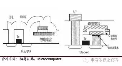
5) FRAM (Ferroelectric RAM)
FRAM (Ferroelectric RAM): Ferroelectric RAM has a structure similar to DRAM, with the basic unit consisting of a MOS transistor and a capacitor. However, the dielectric material in DRAM cannot store charge after power is lost, while FRAM uses a ferroelectric crystal that retains charge even after power loss. When voltage is applied to the planar capacitor, the ferroelectric crystal polarizes under the electric field, forming polarized charges. The polarized charges formed under positive voltage are lower, while those formed under negative voltage are higher, creating a binary stable state suitable for storage. FRAM structures mainly include two types: Planar structures are relatively simple, using LOCOS isolation without requiring CMP, while Stacked structures have higher integration but are more complex, requiring STI (Shallow Trench Isolation) and CMP.
Figure 18: Two Mainstream FRAM Structures
Advantages of FRAM: Combining the high-speed read/write advantages of DRAM with the non-volatility of Flash.
Disadvantages of FRAM: The biggest drawback is poor miniaturization capabilities, making it difficult to adopt nanometer-level processes. Additionally, no perfect ferroelectric crystal material has yet been discovered. The mainstream materials PZT (Lead Zirconate Titanate) and SBT (Strontium Bismuth Titanate) have their drawbacks: PZT can be prepared at lower temperatures using methods like sputtering and MOCVD, has cheap raw materials and low crystallization temperatures, and is easier to integrate into processes, but it suffers from fatigue degradation issues and lead pollution. SBT, while environmentally friendly and free from fatigue degradation problems, has a high fabrication temperature and is challenging to integrate into processes.
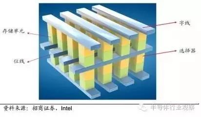
6) Unveiling Intel/Micron’s 3D XPoint Technology
In July 2015, at the Intel Developer Forum (IDF), Intel and Micron jointly released a next-generation memory technology called 3D XPoint. This technology, developed over ten years, has achieved the first practical combination of low cost, high speed, and non-volatility, which Intel describes as a qualitative breakthrough in the storage field since NAND was invented in 1989.
Figure 19: Structure of 3D XPoint
Specifically, the random write speed of 3D XPoint is 1000 times that of NAND, with a density 10 times that of DRAM. Intel also compared the initial actual products using 3D XPoint technology with its top SSD using NAND flash. The results showed that under 8-thread conditions, the 4K random read/write speed of the former was 5.44 times that of the latter, and in single-thread conditions, the gap widened to 7.25 times. Intel stated that this technology has latency higher than flash but slightly lower than memory, allowing for more data to be stored closer to the processor at lower costs, significantly reducing latency and accelerating analysis speed.
In addition to having the non-volatility of flash memory and the high transmission speed of memory, 3D XPoint also has more relaxed etching size requirements and layer addition space, which significantly reduces its preparation costs. For years, Intel and Micron have been suppressed by Japanese and Korean companies such as Samsung, Hynix, and Toshiba in the memory field. The joint launch of this disruptive new memory undoubtedly attracted attention away from the 3D NAND primarily promoted by Samsung and Hynix. In this section of the report, we will conduct a detailed analysis of 3D XPoint, revealing why it possesses such high comprehensive performance, its application scenarios, the challenges it currently faces, and its mass production plans.
Structural Features and Operating Principles
Easy positioning of storage units, soaring random write speeds: NAND Flash cannot pinpoint specific storage units but can only locate the content of a page (approximately 4KiB or 8KiB) at a time, requiring the entire page to be written and the entire block (128 or 256KiB) to be erased, complicating garbage collection algorithms and greatly impacting random access performance. In contrast, in 3D XPoint, 128 billion densely arranged storage units are connected by intersecting word lines and bit lines, enabling each memory unit to be independently accessed through two wires, storing one bit of data. Thus, similar to DRAM, it exhibits excellent random performance.
Unisplendour Partners with Wuhan Xinxin to Accelerate Domestic Memory Development
The semiconductor memory chip industry is a “three high” industry characterized by high technical barriers, high capital barriers, and high concentration. On the surface, it seems to be a hard nut to crack. The country has invested heavily in memory development in recent years, and whether it can achieve the goal of domestic memory production is worth discussing. This chapter will analyze the necessity of developing memory in mainland China from both strategic and economic perspectives.
1) Strategic Significance: The ZTE Incident Rings Alarm Bells Again; Chip Localization is Crucial for National Information Security
Following the 2013 Snowden incident, the ZTE incident in March this year has once again made us realize the urgency of chip localization. ZTE was punished by the US Department of Commerce for allegedly violating US export control policies against Iran. The Department of Commerce ordered a restriction on ZTE’s suppliers in the US from exporting products to ZTE, which could cut off the supply of key components for ZTE’s current system design. Although the US government announced the lifting of the ban after half a month of negotiations, this incident served as a wake-up call for the current state of China’s semiconductor industry.
As a key product in the semiconductor industry, memory chips are carriers of massive data. In an increasingly electronic and data-driven world, data is the “electronic ID card” of every citizen and even a nation, holding strategic importance. As long as we cannot independently master key technologies, we remain subject to others! If relations between the two countries deteriorate or even lead to war, the US government may implement a complete embargo, which would greatly impact our economy and information security. Therefore, speeding up the domestic replacement of memory chips and the entire semiconductor industry is necessary to reduce reliance on developed countries!
2) Economic Significance: The Mainland Memory Chip Market is Approximately $40 Billion, with Greater Potential in Emerging Markets
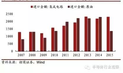
The existing market is about $40 billion: As the largest consumer of integrated circuits, mainland China has a very low market share of its own enterprises, leading to huge consumption and low self-sufficiency, meaning massive imports. In recent years, the import value of integrated circuits has frequently exceeded that of crude oil, making it China’s largest import commodity. Currently, 80% of high-end chips depend on imports, and the profits of chips are highly correlated with their technical content. Therefore, the country must pay a large amount of foreign exchange to countries like South Korea, the US, and Japan every year, with memory being the type of semiconductor product with the lowest self-sufficiency rate among the four major categories. The top three or four foreign companies occupy over 90% of the market for DRAM and NAND memory chips. In the first three quarters of 2015 alone, China purchased $12 billion of DRAM and $6.67 billion of NAND flash, accounting for 21.6% and 29.1% of global consumption, respectively.
Figure 20: Comparison of Integrated Circuit Imports and Crude Oil
Emerging Markets Are Growing Rapidly with Unlimited Potential: Influenced by macroeconomic downturns, the weakening of Moore’s Law, and the exhaustion of the smartphone penetration dividend, the growth rate of traditional semiconductor application markets has slowed. However, the Internet of Things is rising as a new star. In June 2016, the NB-IOT wireless communication technology standard was frozen, tailored for the Internet of Things, featuring broad coverage, numerous connections, low power consumption, and low cost. Its official launch has garnered support from numerous device manufacturers and telecom operators, indicating that the Internet of Things is entering a phase of rapid development. According to Markets and Markets, the global IoT chip market is expected to grow at a compound annual growth rate of 11.5% from 2016 to 2022, with the market size expected to exceed $10 billion by 2022. Most IoT terminals and server ends will require storage chips, especially on the server side, which will be a new growth point for semiconductor memory.
3) Timing: A Rare Opportunity for Technological Upgrades and a Chance to Overtake on the Curve!
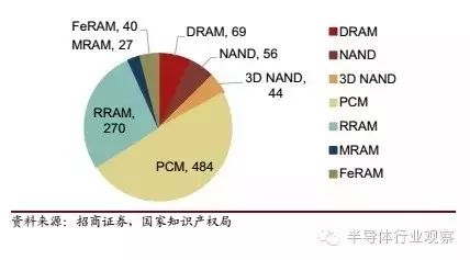
Whether for NAND or DRAM, both are gradually showing signs of fatigue in terms of cost and performance. Therefore, major memory leaders are actively developing new types of memory, which still face many technical challenges. However, challenges always coexist with opportunities. The traditional memory market has shown a highly monopolized form, and the degree of monopoly has been gradually increasing in recent years. In contrast, new types of memory differ significantly in architecture and materials, and the progress of major memory manufacturers has not been smooth. Under strong national policy support, domestic institutions have achieved significant results: In the field of 3D NAND, Wuhan Xinxin has partnered with Spansion, achieving 9 layers; in new memory types such as PCM and RRAM, many domestic companies and research institutions are also exploring. From the perspective of patent numbers, DRAM and NAND have formed high patent barriers due to high industry monopolization. Companies like Samsung, Hynix, Toshiba, and Micron have accumulated patents over the years. In contrast, new memory leaders do not hold absolute advantages, and there are opportunities for domestic companies to make their mark in many subfields. Currently, the number of patents in new types of memory in China has greatly exceeded that of DRAM and NAND, and the gap with domestic leading enterprises is relatively small.
Figure 21: Patent Application Data for Traditional and Emerging Storage in Mainland China
Now is a once-in-a-decade opportunity for technological updates and innovations. China should seize this opportunity, vigorously support relevant enterprises and research institutions, and strive to achieve curve overtaking. If missed, once other companies establish patent and scale barriers again, it will be much more costly for China to enter this field.
Future Layout: Focus on Three Leading Companies
To avoid excessive resource dispersion leading to waste or unnecessary competition, China should focus on cultivating 1-2 leading enterprises in the memory field, emphasizing both technological research and capital operations. Under the guidance of national policy, strong companies should unite, creating a virtual IDM model where leading companies in the upstream, midstream, and downstream collaborate closely for mutual development. Currently, three key forces have formed in the domestic memory development sector, aiming to achieve domestic substitution of memory within several years or more and capture some overseas markets.
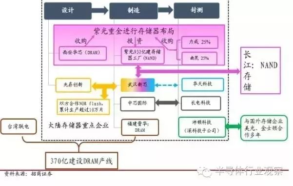
1) Unisplendour Group Acquires Wuhan Xinxin, Establishes Changjiang Storage
In November 2015, Unisplendour National Chip (formerly Tongfang National Chip) announced the largest ever A-share private placement plan, investing 93.2 billion yuan in the memory chip field (of which 60 billion yuan is raised) to build a memory chip factory mainly for producing flash memory chips. In February 2016, Unisplendour announced it would purchase 25% of the shares of Powerchip Technology for 3.79 billion yuan and 25% of the shares of Nanya Technology for 2.34 billion yuan. Powerchip and Nanya are both major packaging and testing plants in the semiconductor memory field, indicating Unisplendour’s clear intention to enter the memory sector.
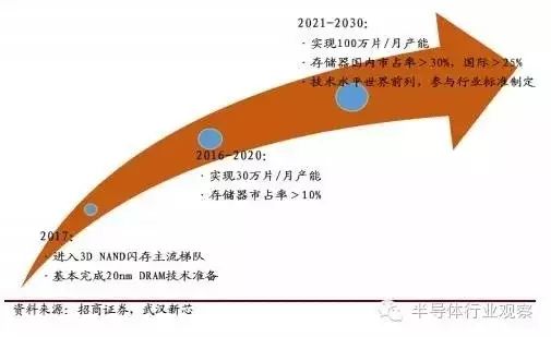
Figure 22: Development Plan for Wuhan Xinxin’s Memory Chips
In March 2016, the Big Fund signed an agreement with the Hubei Provincial Integrated Circuit Industry Investment Fund, the National Development Fund, and the Hubei Provincial Science and Technology Investment Group, investing $24 billion to boost Wuhan Xinxin’s focus on developing 3D NAND memory.
2) Fujian Jin Hua Partners with Taiwan UMC to Collaborate on DRAM Plans
In May 2016, Fujian Jin Hua Integrated Circuit Co., Ltd. announced a partnership with UMC to combine Taiwan’s semiconductor manufacturing capabilities with mainland China’s market and capital. UMC will conduct R&D on 32nm process technology in Taiwan, while Jin Hua will provide DRAM-specific equipment and pay technical remuneration based on development progress. The results will be jointly owned by both parties. The technology developed in this collaboration will primarily be used for niche DRAM production.
On July 16, the Fujian Jin Hua memory integrated circuit production line was officially launched in Quanzhou Jinjiang. The first phase of the project involves an investment of 37 billion yuan, with an expected monthly production capacity of 60,000 12-inch memory wafers by September 2018 and an estimated annual sales of $1.2 billion, primarily for niche DRAM production. The second phase of the project will expand to a monthly production capacity of 120,000 wafers within five years.
This collaboration focuses on niche DRAM as a breakthrough point for two main reasons: first, because its technology development is relatively easier; second, because this type of DRAM serves a niche market for special applications, where Samsung and Hynix typically focus on standard DRAM and do not have fixed production lines for niche DRAM, allowing Jin Hua and UMC to better serve this market.
3) Hefei Government’s Multi-faceted Layout to Develop DRAM
The Hefei government has always placed great importance on the development of the semiconductor industry. As early as October 2013, the Hefei Municipal Government issued the “Hefei Integrated Circuit Industry Development Plan (2013-2020)”, which mentioned that Hefei would focus on developing chip design and specialty wafer manufacturing, planning to build 3-5 specialty 8-inch or 12-inch wafer production lines by 2020, achieving a comprehensive production capacity of over 100,000-150,000 pieces/month.
In April 2015, it was reported that BOE, a leading panel manufacturer, planned to enter the DRAM field and announced in October that it would collaborate with Zhaojin Technology, a DRAM design company founded by former members of Elpida, which was acquired by Micron in 2012, to develop DRAM technology.
In February 2016, according to NHK reports, the Hefei government was said to be collaborating with Zhaojin Technology, with the Hefei government initially investing 80 billion yen (approximately 46 billion yuan), while Zhaojin Technology was responsible for factory equipment introduction and production planning. The factory is currently under construction, with the first step being to design low-power DRAM chips for IoT technology. Production is expected to begin in 2018, with a monthly output of 100,000 pieces anticipated.
Figure 23: Relationship Diagram of Key Domestic Memory Companies
Public Account ID: imecas_wx
Long press to identify the QR code to follow us