IntroductionIntroduction
A new week of EDA dynamics is here! Mergers and acquisitions in the EDA industry are ongoing, with many companies collaborating to break through new technologies. This issue will keep you informed!
Headline FocusHeadline Focus
Cadence Partners with NVIDIA to Innovate Power Analysis Technology
Cadence collaborates with NVIDIA to achieve significant breakthroughs in pre-silicon power analysis: leveraging Cadence’s Palladium Z3 Enterprise Emulation Platform and the new Dynamic Power Analysis (DPA) application, hardware-accelerated dynamic power analysis of billion-gate AI designs can be completed in hours, covering billions of cycles with an accuracy of 97%.
This breakthrough addresses the limitations of traditional tools, which can only support calculations for hundreds of thousands of cycles, are time-consuming, and cannot accurately predict power consumption in real scenarios. It can help developers focused on AI, ML, and GPU-accelerated applications design more energy-efficient systems, reducing time to market. This technology can validate functionality, power, and performance during the early design phase and before tape-out, avoiding project delays, and has been integrated into Cadence’s analysis and implementation solutions. Executives from both sides emphasized the importance of this collaboration in driving the development of related technologies.
Changxin and Changjiang Adopt Domestic EDA
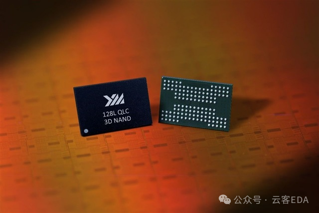
As Changxin Memory and Changjiang Storage ramp up the mass production of DRAM and NAND flash, the focus of the chip industry is gradually shifting to the foundational aspects of chip development: replacing reliance on overseas products with domestic electronic design automation (EDA) tools.
In this replacement process, the storage full-process EDA tool system developed by Huada Jiutian has been applied in the chip development phase at Changjiang Storage’s Wuhan factory. By covering efficient solutions from schematic design to layout development, it not only shortens the chip design cycle but also ensures that design results can seamlessly transition to mass production through precise process adaptation and PDK (Process Design Kit) development capabilities, providing support for the large-scale production of storage chips.
Another significant breakthrough comes from Xinha and Semiconductor’s ecological collaboration with Kirin Software. The EDA tools and operating systems certified by both parties achieve full-chain technical adaptation from chip design to packaging testing to system applications, covering mainstream design needs.
Among them, Xinha Semiconductor’s 2.5D/3D advanced packaging simulation platform Metis effectively addresses the complex electromagnetic coupling issues arising in high-density interconnect structures, providing assurance for the research and mass production of Changjiang Storage’s high-stacking NAND flash, helping to break through the bottlenecks in advanced storage chip packaging technology.
NVIDIA Plans to Supply New AI Chip “B30A” to China
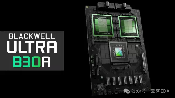
NVIDIA is developing a new AI chip B30A for the Chinese market, with plans to provide test samples to Chinese customers as early as September 2025, outperforming the currently approved H20 chip.
This chip features a single-chip design, with computing power about half that of the flagship B300 accelerator card’s dual-chip configuration, equipped with high-bandwidth memory (HBM) and NVLink technology to enhance data transfer efficiency, likely modified from the single-chip design of the Blackwell B300A. The single-chip design reduces the risk of being classified as a “high-performance computing device,” thus avoiding stricter export scrutiny while maintaining the advanced nature of the Blackwell architecture.
On the technical side, the B300A adopts TSMC’s 4nm process, equipped with 144GB HBM3E high-bandwidth memory, with a power consumption of 600W. As the “single die version” of the B300, although performance is reduced, the generational advantages of the Blackwell architecture are expected to significantly outperform the theoretical performance and energy efficiency of the H20 based on the previous Hopper architecture. However, its specifications have not yet been fully finalized.
The market positioning of the B300A is clear, aiming to provide performance exceeding that of the H20 while complying with the U.S. Department of Commerce’s Export Administration Regulations (EAR) to meet the AI computing needs of the Chinese market and competition from local manufacturers.
Arm Heavily Recruits Amazon AI Chip Experts
Arm has announced the hiring of Rami Sinno, head of Amazon’s AI chip division, to accelerate its plans for self-developed complete chips.
This move marks Arm’s strategic shift from the traditional chip intellectual property (IP) licensing model to the independent design and manufacturing of complete chips.Arm aims to enhance its competitiveness in the rapidly growing AI computing market through self-developed chips.
Currently, Arm primarily generates revenue by selling core architectures and instruction sets for chip designs to clients such as Apple and NVIDIA, who use Arm’s technology to design their chips. However, Arm has been actively investing part of its profits into developing its own chips and other components.
It is reported that Arm has hired several experienced executives and experts to support its self-developed chip plans, including former HP executives with extensive system design experience, Nicolas Dube, and chip engineers Steve Halter, who previously worked at Intel and Qualcomm.
Previously, Arm’s self-developed chip plans had attracted widespread attention and discussion within the industry. On one hand, this strategic shift could bring new market opportunities, but it may also face competitive relationship issues with existing clients. Additionally, Arm needs to invest significant resources in technology research and development, manufacturing, and marketing to ensure the success of its self-developed chip projects.


Tech InsightTech Insight
Huada Jiutian Launches Advanced Packaging Design Platform Storm
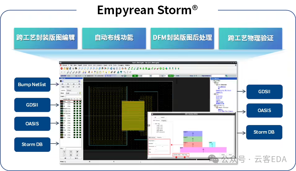
Huada Jiutian has launched the advanced packaging layout design solution Empyrean Storm®, an innovative EDA tool aimed at addressing pain points in advanced packaging design such as complex routing, low tool efficiency, DFM processing, and cumbersome physical verification, significantly improving design efficiency.
Basic functions and adaptability:
Supports cross-process packaging layout data import and design editing, deeply adapts to mainstream processes such as Silicon Interposer and Organic RDL; can achieve large-scale automatic routing for multi-chip communication protocols like HBM and UCIe; can complete DFM layout post-processing such as Dummy filling, and features seamlessly integrated cross-process physical verification Argus, ensuring layout correctness through DRC/LVS checks.
Automatic routing capabilities:
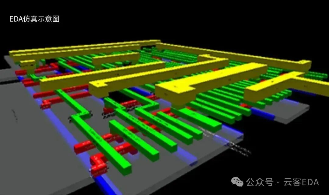
In traditional chip design, manual routing of modules like HBM and UCIe requires handling hundreds of thousands of high-density interconnect lines, which can lead to crosstalk and timing violations. Storm is equipped with an intelligent automated routing engine, allowing users to configure rules and trigger commands to initiate automatic routing. Core capabilities include cross-layer routing in silicon-based interposers, global RDL and power network routing in organic interposers, supporting diverse routing angles, and generating 3D routing diagrams to visually present line paths.
DFM layout post-processing capabilities:
To ensure mass production, it features intelligent metal dummy filling (supporting special shapes), automatic droplet processing (enhancing connection reliability), and packaging test structures (Daisy Chain) modules (automatically completing connections and analysis, quickly locating anomalies), improving design manufacturability and product yield.
One-stop design platform:
Covers the entire design process, including full-featured layout editing (supporting lossless import and export of multiple GDSII/OASIS data, breaking through the limitations of traditional flat editing, supporting 3D stacked display editing), real-time analysis and checks (cross-chip net tracing, checking signal connectivity in advance), seamlessly integrated verification tools (linked with Argus, providing full-process verification), and version data comparison (efficiently comparing version differences, quickly identifying changes), enhancing design fluidity and process optimization efficiency.
Practical application efficiency and customer feedback:
When handling high-speed interfaces like HBM and UCIe, traditional tools require 60-90 days, while Storm can complete IO quantities of 200K for Micro-bumps and TSV cross-layer routing in 15 days; in customer cases, design iterations only take 10 minutes, effectively solving bottlenecks in advanced packaging design and improving efficiency by 1-2 months.
China UpdateChina Update
Huada Jiutian’s Full-Process EDA System Achieves Major Breakthroughs
As one of the three core categories of integrated circuits, it accounts for over a quarter of the chip industry market and is crucial for promoting technological progress and ensuring industrial security.
As a leading domestic EDA provider, Huada Jiutian has launched the only full-process EDA solution in China that supports large-scale Flash/DRAM mass production, providing one-stop services for design, verification, and mass production. This solution innovates in fully customized design platforms and physical verification, breaking through the bottlenecks of traditional design models in massive arrays and complex signal processing, ensuring the reliability and success rate of ultra-large-scale storage chip tape-outs, meeting stringent requirements for storage density, performance, and delivery efficiency, while breaking foreign monopolies and supporting the sustainable development of the domestic storage chip market, promoting the rise of related industries in China.
Products include fully customized design platforms (including various full-process tools for storage circuits), digital circuit design, wafer manufacturing, advanced packaging, 3DIC design, and other EDA tools, as well as basic IP and wafer manufacturing engineering services, mainly applied in the fields of integrated circuit design, manufacturing, and packaging.
Sawei Acquires Zhancheng Technology, Expanding Chip Design and EDA Business
Sawei Electronics recently acquired 56.24% of Qingdao Zhancheng Technology for 157 million yuan, holding a total of 61% of its shares after the transaction, achieving control, adding MEMS chip design services and EDA software development to its business. Zhancheng Technology is a national high-tech enterprise and has multiple qualifications such as specialized and innovative “key small giant” enterprises.
The two parties have a solid foundation for cooperation; in 2022, Sawei Electronics’ subsidiary strategically invested 5 million yuan in Zhancheng Technology, and over the past three years, they have engaged in in-depth exchanges on industrial collaboration, forming a consensus on the development of the MEMS industry. Zhancheng Technology has rich experience in parasitic parameter extraction, which can collaborate with Sawei Electronics in MEMS EDA field research and development, enhancing its comprehensive competitiveness in the MEMS chip manufacturing field.
This transaction will help Sawei Electronics expand and deepen its layout in the MEMS chip manufacturing and design services field, leveraging Zhancheng Technology’s resources to promote industrial ecological collaboration through the “MEMS+” model, enhancing comprehensive competitiveness; at the same time, Zhancheng Technology has a foundation for performance growth, and Sawei Electronics will drive business integration through mergers and acquisitions, improving the performance and sustainable profitability of the listed company, creating medium- to long-term returns for shareholders.
Huahong Semiconductor Acquires Huali Micro to Resolve Competitive Dilemma
Huahong Semiconductor is planning to acquire a controlling stake in its brother company Huali Micro through the issuance of shares and cash payment, targeting the equity of Huali Micro’s factory that competes with Huahong in 65/55nm and 40nm processes, which is currently in the separation stage. This acquisition is part of a planned strategic integration, primarily aimed at resolving historical competitive issues.
Huahong Semiconductor and Huali Micro both belong to the Huahong Group, with the former being a global leader in specialty process wafer foundry, while the latter focuses on advanced logic processes and specialty process platforms. Initially, the two had different positions, but as the 65/55nm process has become mainstream in multiple fields, both have overlapping business in the 65-55nm and 40nm nodes, especially Huali Micro’s Huahong Five Factory (12-inch production line, covering processes from 65/55nm to 40nm) overlaps with Huahong Semiconductor’s Huahong Seven and Nine factories. When Huahong Semiconductor went public on the Sci-Tech Innovation Board in 2023, the Huahong Group had already committed to injecting Huali Micro within three years to eliminate competition, and the preliminary identified transaction counterparties include the Huahong Group and related investment funds.
If the acquisition is successful, Huahong Semiconductor’s 12-inch wafer foundry capacity will be significantly enhanced, and after integration, it will have three 8-inch production lines and three 12-inch production lines. Currently, Huahong Five Factory has a monthly capacity of 38,000 wafers, Huahong Seven Factory has a monthly capacity of 40,000 wafers (planned for 94,000 wafers), and Huahong Nine Factory is planned for a monthly capacity of 83,000 wafers. In the long run, the total capacity for 12-inch wafers is expected to reach 215,000 wafers, helping it maintain its leading position in global specialty process foundries and form economies of scale. Currently, 12-inch wafers have become mainstream in the market due to cost and adaptability advantages, aligning with the demands of emerging fields, while Huahong Semiconductor holds a leading position in the mainland wafer foundry sector..

Tech PicksTech Picks
Automotive Chip Development: The Secrets Behind Arm Zena CSS
As automotive electronics evolve towards integration and AI deeply penetrates core scenarios, Arm has launched the Zena Compute Subsystem (CSS) to respond to industry demands and challenges.
The development of automotive electronics and the core position of AI:
Automotive electronics are transitioning from decentralized ECUs to domain controllers, central vehicle computing ECUs, with AI deeply integrated into core scenarios such as ADAS, intelligent cockpits, and vehicle control, becoming a core element defining automotive competitiveness.
The launch and goals of Arm Zena CSS:
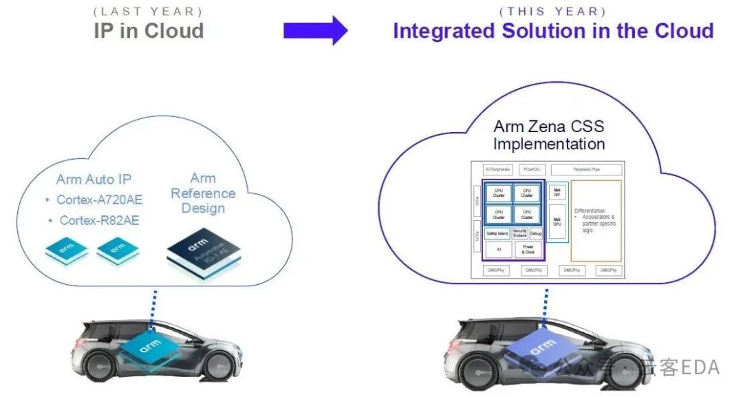
Arm has introduced the Arm Zena Compute Subsystem (CSS) as a standardized and pre-integrated computing platform, aiming to shorten development cycles, allowing software teams to start development early, helping automakers launch new models at least a year ahead of schedule.
The core demands of the “AI Defines Automotive” era:
Suraj points out three major demands, namely innovative flexibility (ensuring safety and flexibility in integrating new AI applications), scaling AI applications (scaling applications across the entire ecosystem), and shortening time to market (to cope with rapid iterations of AI technology).
Challenges faced by the industry:
The next generation of autonomous driving SoCs is complex, with high costs for hardware and software development, and limited reusability across different vehicle platforms, leading to increased costs and extended mass production cycles.
The core features of Arm Zena CSS:
It is not a simple IP combination but a computing subsystem in the form of pre-verified RTL design packages, integrating advanced technologies (such as 16 Cortex-A720AE CPU clusters), compliant with ISO 26262 and ISO 21434 certifications, saving 12 months of chip development time and reducing engineering resources by about 20%.
Using a modular architecture, it can expand functions as needed (such as adding camera modules, NPUs, etc.), adapting to diverse scenarios such as L2+ level ADAS, intelligent cockpits, and autonomous driving; core computing modules can be reused, reducing cross-project development costs.
Development cycles and ecosystem:
Collaborating with partners like AWS and Cadence to build virtual prototype platforms and cloud-native development frameworks, shortening software development cycles by 2 years compared to traditional processes, significantly improving product launch efficiency when combined with shortened chip development time.
Relying on organizations like SOAFEE, along with numerous partners such as Red Hat and Sailun AI, to establish standards and develop functions like ADAS and voice interaction, supporting open and extensible software development.
The significance of Zena CSS:
It marks the upgrade of automotive computing platforms from single IP supply to integrated, scenario-based solutions, providing important value to chip manufacturers (simplifying design), automakers (achieving hardware standardization and expansion), software ecosystems (providing efficient development environments), and car owners (enjoying AI innovations faster).

If you are interested in our content, please continue to follow us~
Welcome to comment and leave messages, see you next week at the same time!
Yunke EDA focuses on the forefront, inviting you to explore technological changes together