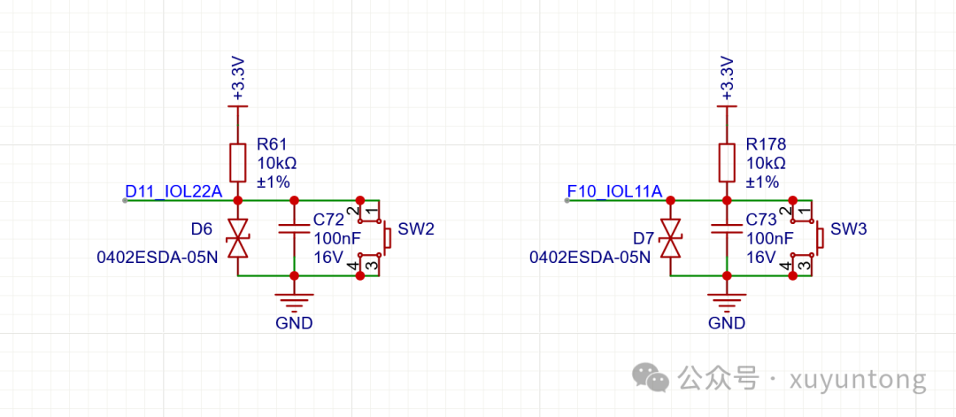
Following the previous article, Verilog *1* SPI – Development, we have simulated the design, but we have yet to see how it looks on the actual circuit. Without hands-on experience, it remains theoretical; simulation is merely a tool to expedite the actual circuit development, and we must not lose sight of that. First, let’s take a look at the schematic of the Logic Pie G1. Below is the schematic from JLC, which can be opened directly in a web browser. For convenience, I have taken a screenshot, as shown in Figure 1.
https://pro.lceda.cn/editor#id=61327d881e5f4f0c834908cf28c3eb08,tab=1199dcbe5a844fe5a8a074140edc99f8|*1199dcbe5a844fe5a8a074140edc99f8@61327d881e5f4f0c834908cf28c3eb08
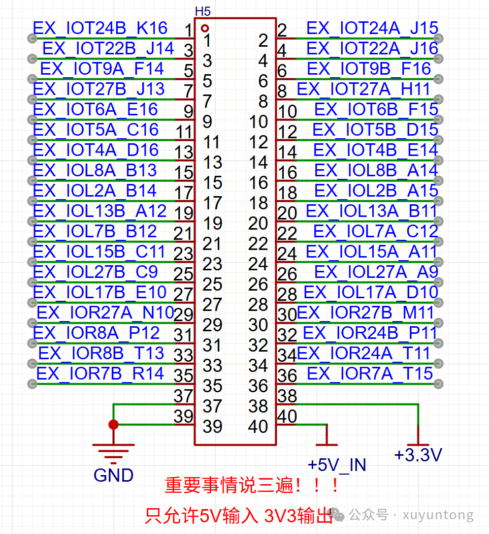
Figure 1: FPGA IO Pins
With Figure 1, we can get started!
Creating a New Project
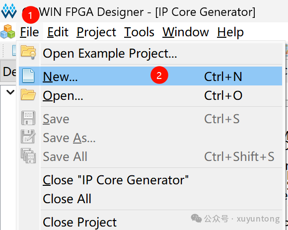
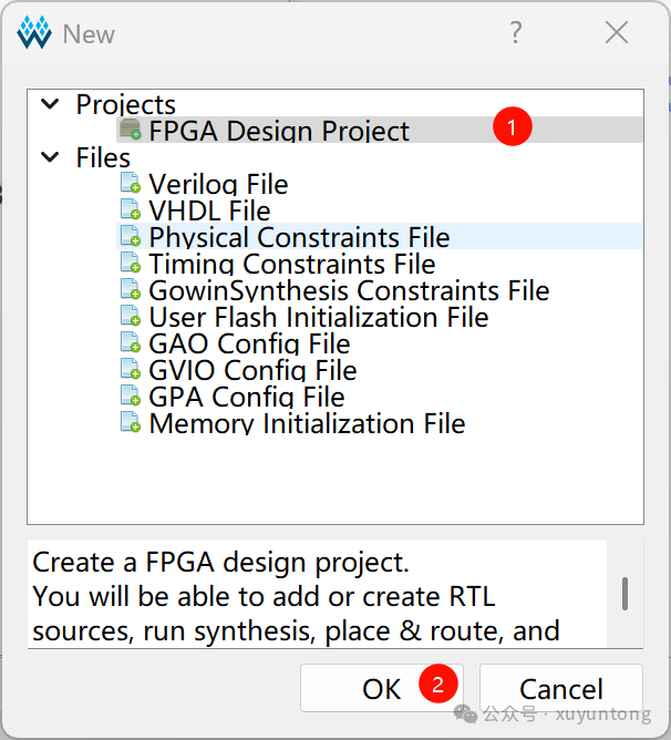
File->New
FPGA Design Project ->OK
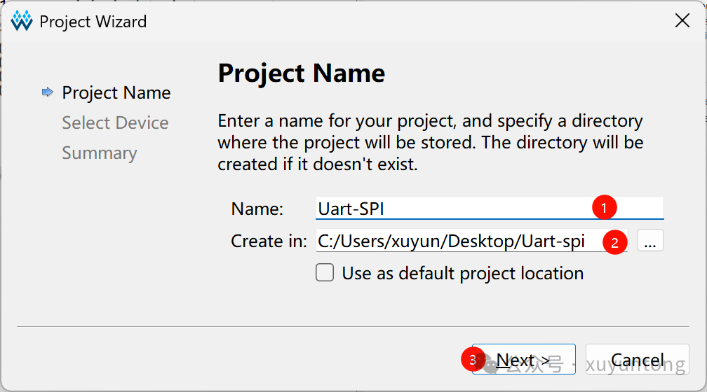
1. Name -> Give it a name
2. Create in -> File location
3. OK
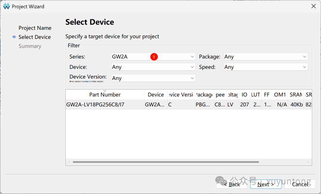
Next, we select the model:
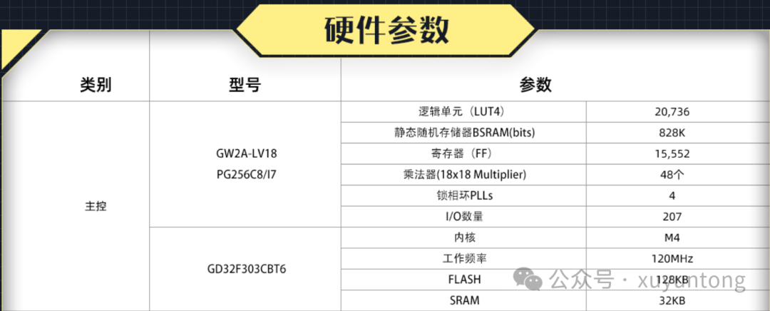
As of now, there is only one model under GW2A. After selecting, proceed directly to Next to complete the project setup.
Copying the Code
module SPI ( input clk, input rst, input transFlag, output reg cs, output reg mosi, output reg sclk);// Define states// localparam is valid only within the module, `define is globally validlocalparam IDLE = 1'b1;localparam Trans = 1'b0;reg [1:0] Current_S;reg [1:0] Next_S;reg [4:0] Trans_Cnt;reg [1:0] sclk_status;reg [7:0] Data;reg [4:0] clk_div_cnt; // Clock division counterreg spi_clk; // Divided clock signal// 25 times clock division logicalways @(posedge clk or negedge rst) begin if (!rst) begin clk_div_cnt <= 5'b0; spi_clk <= 1'b0; end else begin if (clk_div_cnt == 5'd24) begin // Reset counter when counting to 24 clk_div_cnt <= 5'b0; spi_clk <= ~spi_clk; // Toggle divided clock signal end else begin clk_div_cnt <= clk_div_cnt + 1'b1; end endendinitial begin sclk <= 1'b0; Trans_Cnt <= 5'b0; sclk_status <= 2'b00; Data <= 8'h55; mosi <= 1'b0; Current_S <= IDLE; cs <= 1'b1; Next_S <= IDLE;end// Use divided clock signal for state transitionalways @(posedge spi_clk or negedge rst) begin if (!rst) begin // Jump to IDLE state Current_S <= IDLE; end // Jump to next state else begin Current_S <= Next_S; endend// Use divided clock signal for state machine logicalways @(posedge spi_clk or negedge rst) begin if (!rst) begin // Reset logic cs <= 1'b1; sclk <= 1'b0; Trans_Cnt <= 5'b0; sclk_status <= 2'b00; Data <= 8'h55; Next_S <= IDLE; end else begin case(Current_S) Trans: begin cs <= 1'b0; // Send one bit of data on each rising edge, increment sclk status case(sclk_status) 2'b00: begin sclk <= 1'b1; sclk_status <= sclk_status + 1'b1; end 2'b01: begin mosi <= Data[7]; Data <= Data << 1; sclk_status <= sclk_status + 1'b1; end 2'b10: begin sclk <= 1'b0; sclk_status <= 2'b00; Trans_Cnt <= Trans_Cnt + 1'b1; end endcase // If 8 clocks have been sent, jump to idle in the next cycle if(Trans_Cnt == 5'd8) begin Next_S <= IDLE; Trans_Cnt <= 5'b0; end end IDLE: begin cs <= 1'b1; sclk <= 1'b0; Trans_Cnt <= 5'b0; sclk_status <= 2'b00; // When clk posedge jump to next status if (transFlag) begin Next_S <= Trans; Data <= 8'h55; end else begin Next_S <= IDLE; end end default: Next_S <= IDLE; endcase endendendmoduleSynthesis and Pin Binding
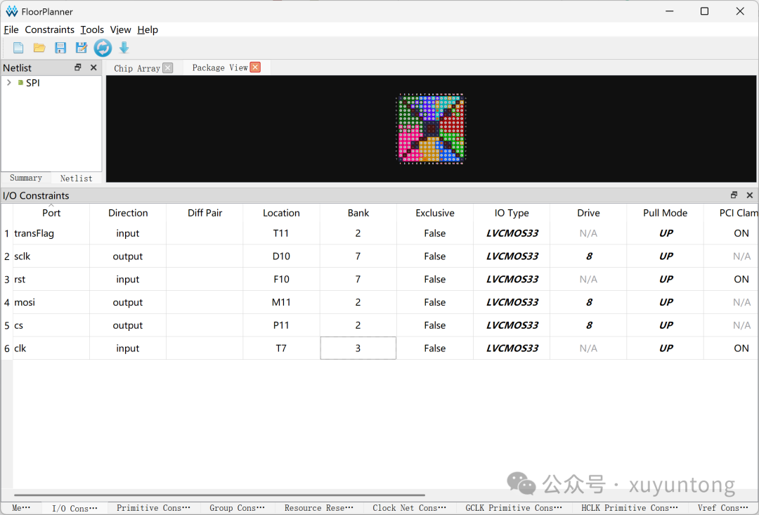
4.1 Determine a pin to use as the reset pin:
Button SW2–D11_IOL22A
Button SW3–F10_IOL11A
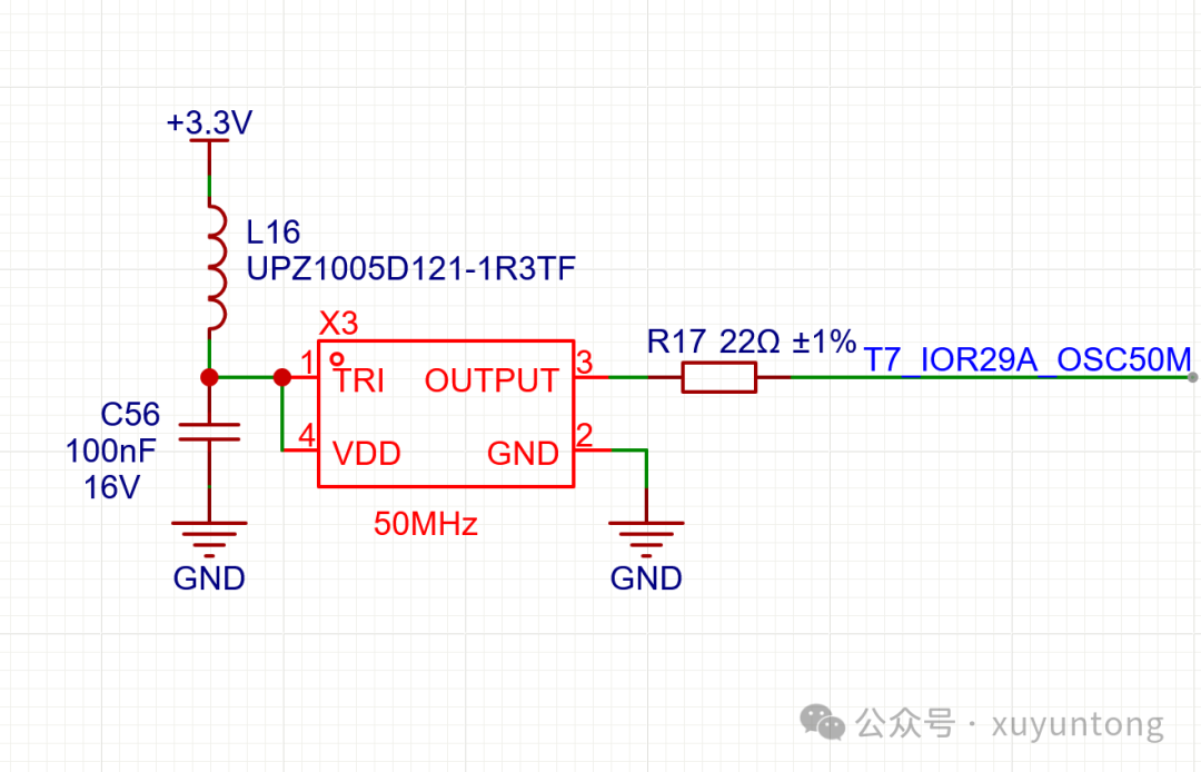
Crystal XTAL– T7_IOR29A
4.2 Determine IO type
Different IO TYPE characteristics are as follows (generated by Qianwen):
- LVCMOS (Low Voltage CMOS)
- LVTTL (Low Voltage Transistor-Transistor Logic): Similar to LVCMOS, but follows TTL logic level standards, mainly used in applications that require compatibility with traditional TTL logic levels.
- SSTL (Stub Series Terminated Logic): Designed for high-speed memory interfaces, such as DDR SDRAM, it improves signal integrity by reducing signal reflections.
- HSTL (High-Speed Transceiver Logic): A standard for high-speed data transmission, commonly used in memory interfaces and communication buses.
- PCIe (Peripheral Component Interconnect Express): A high-speed serial computer expansion bus standard used to connect multiple peripheral devices on a motherboard.
- GTX/GTH/GTY: These are high-speed serial transceivers in the Xilinx FPGA series, designed to support very high data rates, suitable for applications such as Ethernet, Fibre Channel, and SONET.
- MIPI (Mobile Industry Processor Interface): A standard for mobile industry processor interfaces, including CSI (Camera Serial Interface) and DSI (Display Serial Interface), used for camera and display modules in mobile devices.
- JESD204: A standard for high-speed serial interfaces between data converters and FPGAs, particularly suitable for data transmission of ADCs (Analog-to-Digital Converters) and DACs (Digital-to-Analog Converters).
Since we will be testing with a 3.3V UART, we will select LVCMOS33 here.
Test Results
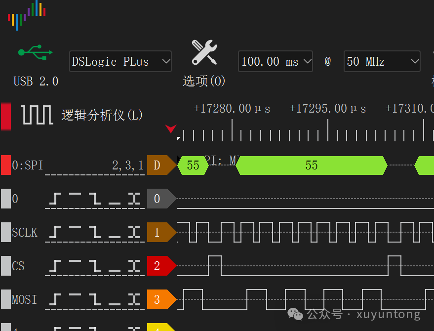
Observing the test results, the falling edge transmission is fine, but there is no gap between CS and SCLK, which looks odd. Let’s add something to adjust it.
Revised Code:
module SPI ( input clk, input rst, input transFlag, output reg cs, output reg mosi, output reg sclk);// Define states// localparam is valid only within the module, `define is globally validlocalparam IDLE = 1'b1;localparam Trans = 1'b0;reg [1:0] Current_S;reg [1:0] Next_S;reg [4:0] Trans_Cnt;reg [1:0] sclk_status;reg [7:0] Data;reg [4:0] clk_div_cnt; // Clock division counterreg spi_clk; // Divided clock signalreg [4:0] delay_cnt; // Delay counterreg delay_start; // Delay start flag// 25 times clock division logicalways @(posedge clk or negedge rst) begin if (!rst) begin clk_div_cnt <= 5'b0; spi_clk <= 1'b0; end else begin if (clk_div_cnt == 5'd24) begin // Reset counter when counting to 24 clk_div_cnt <= 5'b0; spi_clk <= ~spi_clk; // Toggle divided clock signal end else begin clk_div_cnt <= clk_div_cnt + 1'b1; end endendinitial begin sclk <= 1'b0; Trans_Cnt <= 5'b0; sclk_status <= 2'b00; Data <= 8'h55; mosi <= 1'b0; Current_S <= IDLE; cs <= 1'b1; Next_S <= IDLE; delay_cnt <= 5'b0; delay_start <= 1'b0;end// Use divided clock signal for state transitionalways @(posedge clk or negedge rst) begin if (!rst) begin // Jump to IDLE state Current_S <= IDLE; end // Jump to next state else begin Current_S <= Next_S; endend// Use divided clock signal for state machine logicalways @(posedge spi_clk or negedge rst) begin if (!rst) begin // Reset logic cs <= 1'b1; sclk <= 1'b0; Trans_Cnt <= 5'b0; sclk_status <= 2'b00; Data <= 8'h55; Next_S <= IDLE; end else begin case(Current_S) Trans: begin // If 8 clocks have been sent, jump to idle in the next cycle if(Trans_Cnt > 5'd7) begin Next_S <= IDLE; Trans_Cnt <= 5'b0; end else begin // Send one bit of data on each rising edge, increment sclk status case(sclk_status) 2'b00: begin sclk <= 1'b1; sclk_status <= sclk_status + 1'b1; end 2'b01: begin mosi <= Data[7]; Data <= Data << 1; sclk_status <= sclk_status + 1'b1; end 2'b10: begin sclk <= 1'b0; sclk_status <= 2'b00; Trans_Cnt <= Trans_Cnt + 1'b1; end endcase end end IDLE: begin cs <= 1'b1; sclk <= 1'b0; Trans_Cnt <= 5'b0; sclk_status <= 2'b00; // When clk posedge jump to next status if (transFlag) begin delay_start<=1'b1; end if(delay_start) begin // Setting delay counter if (delay_cnt<5'd2) begin delay_cnt <= delay_cnt + 1'b1; end else begin cs <= 1'b0; Next_S <= Trans; Data <= 8'h55; delay_cnt <= 5'b0; delay_start <= 1'b0; end end else begin Next_S <= IDLE; end end default: Next_S <= IDLE; endcase endendendmoduleRevised Code Test Results
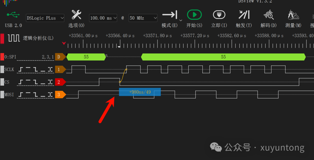
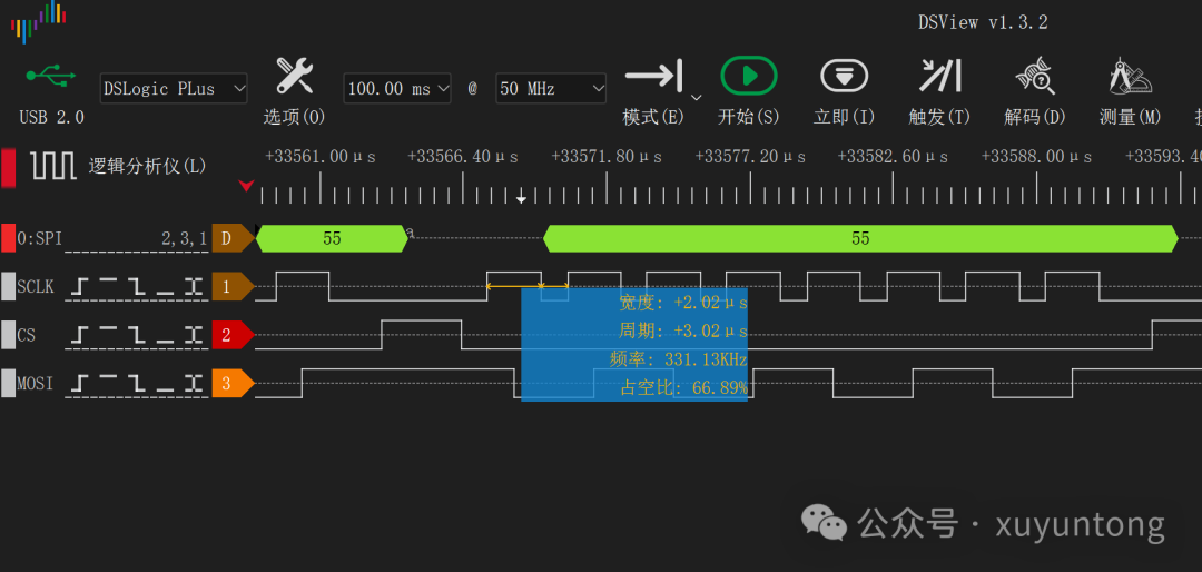
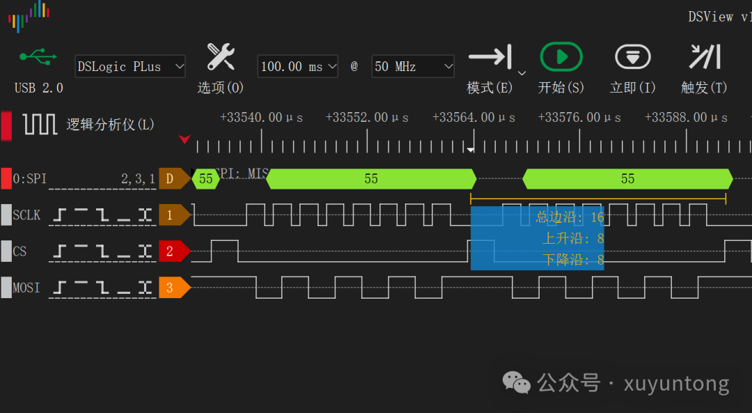
Main modifications:
// Change transmission standard bit to delay flag bit // 修改传输标志位为延时标记位 if (transFlag) begin delay_start<=1'b1; end if(delay_start) begin // Setting delay counter // 设置延迟计数器 if (delay_cnt<5'd2) begin delay_cnt <= delay_cnt + 1'b1; end else begin //jump to Send // 跳转到发送 cs <= 1'b0; Next_S <= Trans; Data <= 8'h55; delay_cnt <= 5'b0; delay_start <= 1'b0; end end else begin Next_S <= IDLE; endEach clock transitions to Next_Status
always @(posedge clk or negedge rst) begin if (!rst) begin // Jump to IDLE state Current_S <= IDLE; end // Jump to next state else begin Current_S <= Next_S; endendReference Document:
https://mp.weixin.qq.com/s/jY0BIhtX8UtWXFMW-xcK2g
Testing Instruments:
Mengyuan Logic Analyzer U2 PLUS
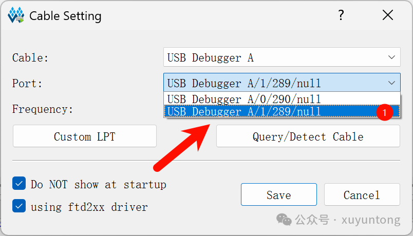
Solution for downloading issues with Gaoyun software:
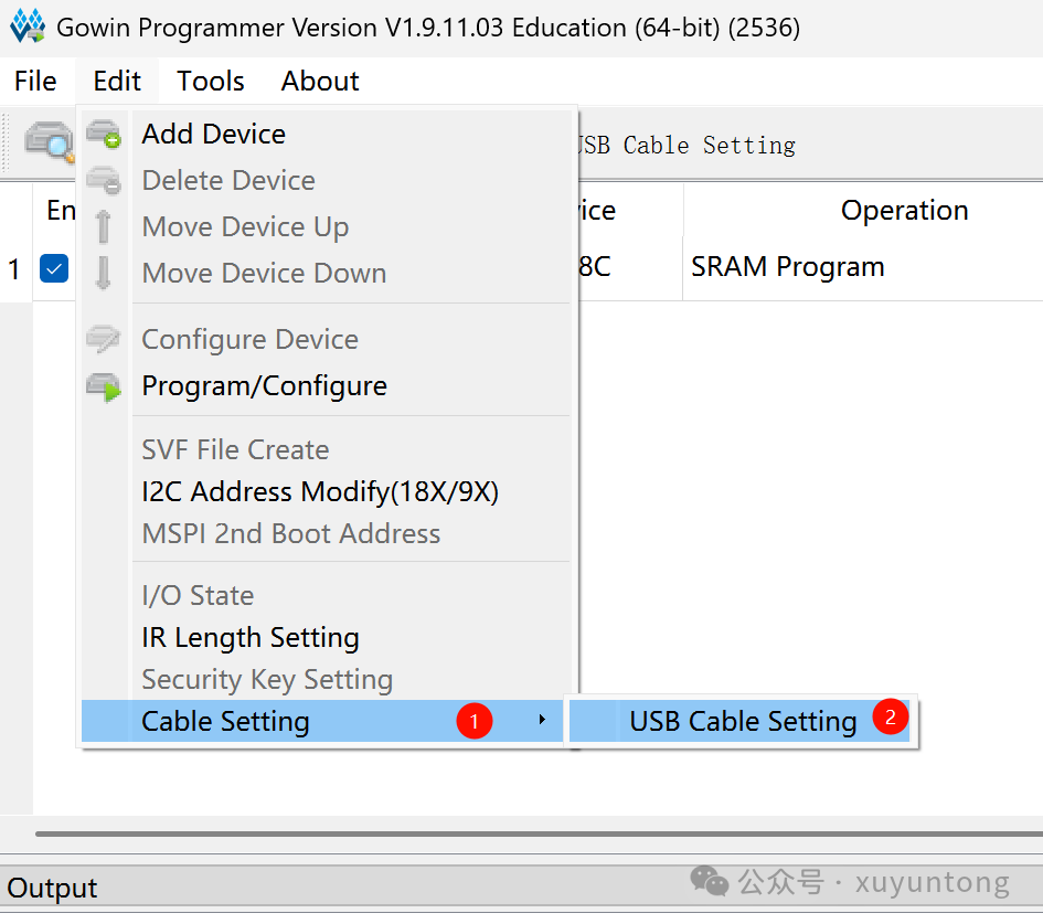
Edit -> Cable Setting -> USB Cable Setting
Need to select USB Debugger A/1