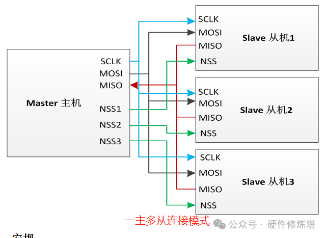
1. Introduction to Serial Peripheral Interface (SPI)The SPI interface (Serial Peripheral Interface) is a widely used high-speed, full-duplex, synchronous serial communication protocol between microcontrollers and peripheral devices.2. Main Features of SPIIt supports master-slave operation in both full-duplex and half-duplex modes; 16-bit width with independent transmit and receive buffers;8-bit or 16-bit data frame formats;Data bit order can be either LSB first or MSB first;Software and hardware NSS management;Hardware CRC calculation, transmission, and verification;Support for DMA mode in transmission and reception.3. SPI Pin DescriptionThe SPI interface is a 4-wire system, with specific descriptions for each pin provided in the table below.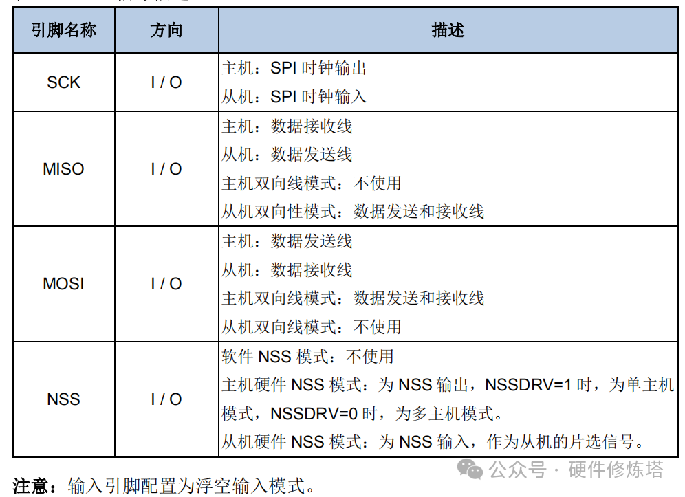 4. SPI Function DescriptionSCK Function: SPI Timing and Data Frame FormatThe CKPL and CKPH bits in the SPI_CTL0 register determine the timing of the SPI clock and data signals. The CKPL bit determines the level of SCK in idle state, while the CKPH bit determines whether the first or second clock edge is the valid sampling edge.In normal mode, the data length is configured through the FF16 bit in SPI_CTL0; when FF16=1, the data length is 16 bits, otherwise it is 8 bits.The data order can be configured by setting the LF bit in SPI_CTL0; when LF=1, SPI sends the LSB first, and when LF=0, it sends the MSB first.NSS Chip Select FunctionNSS, also known as CS (chip select), is the chip select function.Slave ModeWhen configured in slave mode (MSTMOD=0), in hardware NSS mode (SWNSSEN = 0), the SPI obtains the NSS level from the NSS pin, while in software NSS (SWNSSEN = 1), the SPI gets the NSS level from the SWNSS bit. Data can only be sent or received when NSS is low. In software NSS mode, the NSS pin is not used.Master ModeIn master mode (MSTMOD=1), if the application uses a multi-master connection, NSS can be configured as hardware input mode (SWNSSEN=0, NSSDRV=0) or software mode (SWNSSEN=1). Once the NSS pin (in hardware NSS mode) or SWNSS bit (in software NSS mode) is pulled low, the SPI automatically enters slave mode, generating a master configuration error with CONFERR set to 1. If the application wishes to control the SPI slave device using the NSS pin, NSS should be configured as hardware output mode (SWNSSEN=0, NSSDRV=1). After enabling SPI, NSS remains high, and when the transmission or reception process begins, NSS goes low.The application can use a general I/O pin as the NSS pin for more flexible NSS applications.Typically, a pull-up resistor is connected to the NSS pin in hardware, as in hardware NSS mode, the NSS pin does not automatically pull high after data transmission is complete, requiring an external pull-up resistor to ensure it returns to high level correctly. Additionally, the SPI protocol stipulates that when a device is not selected, the NSS pin should remain high. The pull-up resistor ensures that the NSS pin maintains a high state when no other signals are driving it, avoiding uncertain states due to floating pins.In a single master multi-slave SPI system, the NSS pin can be replaced with a regular I/O pin.5. Basic SPI Transmission and Reception Process
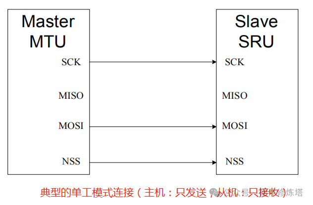
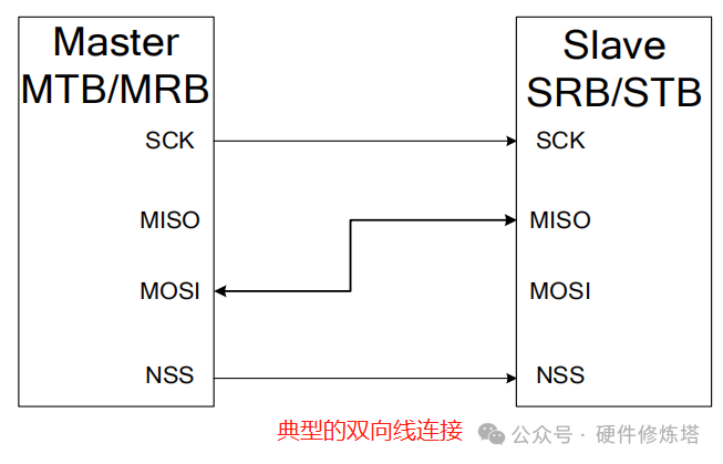
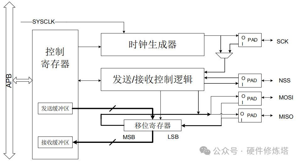 Transmission ProcessAfter completing the initialization process, the SPI module is enabled and remains in idle state. In master mode, when software writes data to the buffer via the APB bus, the transmission process begins. In slave mode, when the SCK signal on the SCK pin starts to toggle and the NSS pin level is low, the transmission process begins. Therefore, in slave mode, the application must ensure that data is written to the transmit buffer before the transmission starts. When the SPI begins to send a data frame, it first loads this data frame from the data buffer into the shift register and then starts sending the loaded data. After the first bit of the data frame is sent, the TBE (Transmit Buffer Empty) flag is set to 1. The TBE flag being set to 1 indicates that the transmit buffer is empty; at this point, if more data needs to be sent, the software should continue writing to the SPI_DATA register. In master mode, to achieve continuous transmission, the software should write the next data to the SPI_DATA register before the current data frame transmission is complete.Reception ProcessAfter the last sampling clock edge, the received data will be stored from the shift register into the receive buffer, and the RBNE (Receive Buffer Not Empty) flag is set to 1. The software reads the received data from the SPI_DATA register, which automatically clears the RBNE flag. In MRU and MRB modes, to receive the next data frame, the hardware needs to continuously send clock signals, while in full-duplex master mode (MFD), the hardware only receives the next data frame when the transmit buffer is not empty.Note: When the SPI is in slave mode, if the number of input clock cycles is not an integer multiple of 8 or 16 (as determined by the configured bit width), and the chip select is disabled, the SPI will not clear the count; after chip select is enabled, it will wait for the corresponding number of clock cycles before transmitting and receiving new data. This issue can be resolved by actively resetting the SPI module through software.There is a very important bus in the block diagram: the APB bus (Advanced Peripheral Bus) is part of the AMBA (Advanced Microcontroller Bus Architecture) bus system, mainly used for low bandwidth, low power peripheral connections. Here is a brief introduction to the characteristics and applications of this bus:6. Characteristics of the APB BusLow Power: The APB bus is designed for low power applications, suitable for connecting low-speed peripherals.Non-Pipelined Design: The APB bus is not pipelined; each transfer requires at least two clock cycles.Simplicity: The APB bus has fewer signals, and the interface design is simple, with all signals related only to the clock rising edge.Single Master Device: The APB bus typically has only one master device (such as an APB bridge), while all other devices are slaves.No Support for Advanced Features: The APB bus does not support burst transfers, outstanding transfers, or simultaneous read/write transfers.7. Applications of the APB BusLow-Speed Peripheral Connections: The APB bus is commonly used to connect low-speed peripherals such as UART, I2C, SPI, timers, etc.Register Configuration: The APB bus is also widely used for configuring registers of various IP modules.System Architecture: In SoC design, the APB bus is usually connected to higher performance buses (such as AHB or AXI) through bridges.8. Typical Operating Modes of SPISPI has four typical operating modes: full-duplex mode, half-duplex mode (master receiving, slave sending), half-duplex mode (master sending, slave receiving), and bidirectional line mode.Full-Duplex Master ModeReferred to as master, it belongs to the MFD (Maximum Frame Duration) mode, while the slave belongs to the SFD (Start of Frame Delimiter) mode. As shown in the figure, the SCK, MIOS, MOSI, and NSS pins of the master and slave are connected correspondingly. The MOSI pin of the master chip indicates the master sending, while the MOSI pin of the slave chip indicates the slave receiving. In other words, the MOSI pin of the master chip is viewed as MO (Master Out), while the MOSI pin of the slave chip is viewed as SI (Slave Input).Other operating modes are similar to full-duplex mode; just ensure the data flow direction is correct.
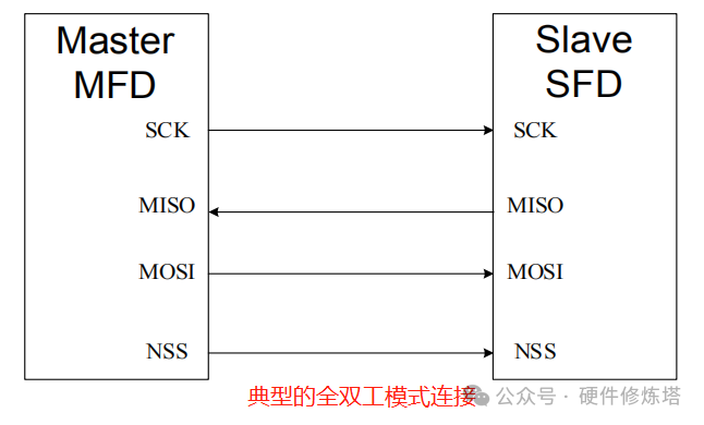
 Here, we summarize the advantages and disadvantages of SPI communication:1. Advantages1). High-Speed Data Transmission• The SPI interface supports high clock frequencies, with data transmission rates typically reaching several megabits per second (Mb/s), and even higher. For example, in some high-performance microcontroller and peripheral communications, the SPI interface can easily achieve data transmission rates of 10 Mb/s or even 50 Mb/s. This high-speed capability makes it very suitable for applications with high real-time requirements, such as high-speed data acquisition systems and image sensor data transmission.2). Full-Duplex Communication• The SPI interface supports full-duplex communication, meaning that the master and slave can simultaneously send and receive data. This allows for efficient data exchange during transmission without waiting for the other party to complete sending or receiving operations. For example, in some communication module applications, the master can simultaneously send commands and receive status information returned from the module via the SPI interface, greatly improving communication efficiency.3). Resource-Saving Pin Usage• The SPI interface requires only four lines (SCLK, MOSI, MISO, CS) to achieve communication. Compared to other communication protocols (such as parallel communication), the SPI interface significantly reduces the number of required pins, which is a great advantage for microcontrollers or system-on-chips (SoCs) with limited pin resources. For example, in some small embedded devices, the number of pins on the microcontroller may be very limited, and using the SPI interface can effectively save pin resources, leaving more space for other functional modules.4). Simple Hardware Design• The hardware design of the SPI interface is relatively simple and does not require complex circuit support. It does not need complicated physical layer circuits like some other communication protocols (such as USB), nor does it require external clock generators or complex signal conditioning circuits. This makes the SPI interface easier to design and implement in hardware, reducing hardware costs and design complexity. For example, in some simple sensor applications, it is sufficient to connect the sensor’s SPI pins to the corresponding pins of the microcontroller and ensure correct power and ground connections to achieve communication.5). Wide Support and Compatibility• The SPI interface is widely supported by almost all mainstream microcontroller and peripheral chip manufacturers. Whether it is ARM Cortex series microcontrollers, STM32 series, or various sensors, memory, and communication module peripheral chips, almost all provide support for the SPI interface. This wide compatibility makes the SPI interface widely used in embedded systems, allowing developers to easily find chips and modules that support the SPI interface, facilitating system design and development.6). Strong Scalability• The SPI interface supports multiple slave devices. By adding additional chip select signals (CS), multiple slave devices can be easily connected to the same SPI bus. This gives the SPI interface strong scalability in systems that require multiple peripheral connections. For example, in a complex embedded system, it may be necessary to connect multiple sensors, memory, and communication modules, and using the SPI interface can achieve these device connections and communications through simple chip select signal extensions.2. Disadvantages1). No Acknowledgment Mechanism• The SPI interface itself does not have a built-in acknowledgment mechanism. During data transmission, the master cannot directly confirm whether the slave has correctly received the data, nor can it determine whether the slave is ready to send data. This may reduce the reliability of data transmission, especially in poor communication environments or when the slave fails. For example, in some long-distance communication or high-noise environment applications, data transmission may be interfered with, and the SPI interface cannot automatically detect and correct these errors.2). Single Master Device Limitation• The traditional SPI interface only supports a single master device. In an SPI bus, there can only be one device acting as the master, while all other devices must act as slaves. This limits the application of the SPI interface in scenarios that require multi-master communication. For example, in some distributed systems, multiple devices may need to act as masters to communicate with slaves, and in such cases, the SPI interface cannot meet the requirements.3). Limited Communication Distance• Since the SPI interface is a high-speed synchronous serial communication protocol, its communication distance is relatively short. Generally, the communication distance of the SPI interface does not exceed a few meters. This is because high-speed signals are easily affected by electromagnetic interference and signal attenuation during transmission, leading to data transmission errors. In some applications requiring long-distance communication, such as remote sensor networks in industrial automation, the SPI interface may not directly meet the requirements and may require additional signal conditioning or relay devices to extend the communication distance.4). Limited Bus Load Capacity• The bus load capacity of the SPI interface is relatively limited. As the number of slave devices connected to the SPI bus increases, the bus load gradually increases, which may lead to signal integrity issues such as signal reflection and crosstalk. These issues can affect the reliability of data transmission and even lead to communication failures. Therefore, when designing an SPI bus system, it is necessary to reasonably control the number of slave devices and take appropriate signal integrity measures, such as adding termination resistors and optimizing wiring. Below is a typical full-duplex application circuit for SPI communication, where RC filtering circuits are added to the SCLK, MOSI, and MISO signal lines to provide some resistance to external interference. If the two chips are very close, and there are space and cost constraints on the PCBA, the RC filtering circuit can be omitted, and the pins of the two chips can be directly connected.
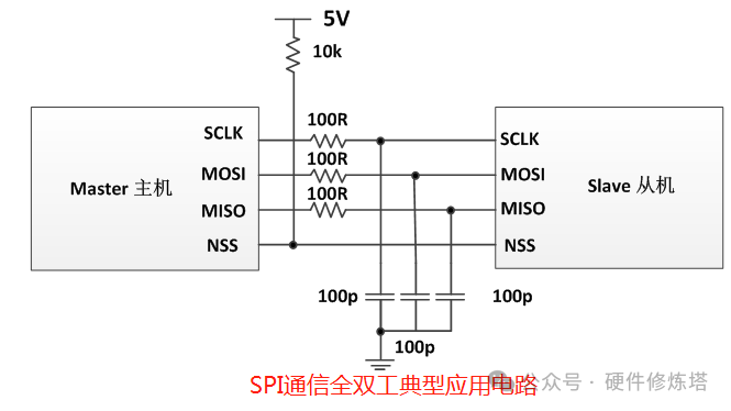 This public account is continuously updated, and everyone is welcome to bookmark and follow. Thank you!