
The computer system is centered around the microprocessor, and all devices must connect to the microprocessor and work in coordination. Therefore, the concept of a bus is introduced in the microprocessor, where all devices share the bus, and at any given time, only one device can send data (multiple devices can receive data simultaneously).
The computer’s bus is divided into three types: control bus, address bus, and data bus. The data bus is used for transmitting data, the control bus is used for transmitting control signals, and the address bus is used for selecting storage units or peripherals.
The 51 series microcontroller has a complete bus interface timing and can expand control objects, with a direct addressing capability of up to 64k (2 to the power of 16).In bus mode, different objects share the bus, independently address, and time-multiplex the bus. The CPU accesses the objects through address selection, completing information transfer between each object.
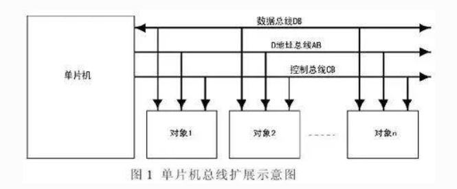
The schematic of the microcontroller’s three-bus expansion is shown in Figure 1.
1. Data Bus
The data bus of the 51 microcontroller is the P0 port, which serves as a bidirectional data channel, allowing the CPU to send and read data from the P0 port.
2. Address Bus
The address bus of the 51 series microcontroller is 16 bits.
To save chip pins, the P0 port is multiplexed. In conjunction with the ALE signal timing, the low 8 bits of the address are sent from the P0 port during the first half of the bus access cycle, while the 8 bits of data are sent from the P0 port during the second half. The high 8 bits of the address are sent through the P2 port.
3. Control Bus
The control bus of the 51 series microcontroller includes read control signal P3.7 and write control signal P3.6, which serve as enable signals for data read and write in bus mode.
The bus timing of the 51 microcontroller is shown in Figure 2.
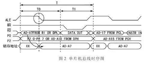
From Figure 2, it can be seen that the operation cycle for a complete bus (read/write) operation is T, where the P0 port is time-multiplexed. During T0, the low 8 bits of the address are sent from the P0 port, and data latching occurs at the falling edge of ALE, sending out the low 8-bit address signal.During T1, the P0 port is used as the data bus to send or read data, and the read/write operation is completed during the low period of the read and write control signals.
It is important to note that during the effective period of the control signals (read and write signals), the high 8 bits of the address are sent from the P2 port, combined with the low 8 bits output from the data latching, achieving a 16-bit address bus, thus addressing within the range of 64kB.
Since the CPU cannot execute read and write operations simultaneously, the read and write signals cannot be effective at the same time.
1. Simple Address Expansion
The P2 port of the 51 microcontroller can be used directly as the high 8-bit address bus. In some simple system circuits, the P2 port is often used for direct addressing to drive.
Below is an analysis of the design of a static digital display circuit using the data buffer 74LS273 as an example, driven by the P2 port.
A single LED digital display unit circuit is shown in Figure 3.
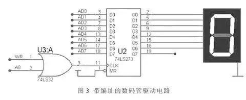
WR and A8 (P2.0) are ORed to provide the clock signal for the 74LS273. When the instruction “MOVX @DPTR, A” is executed, the address information is determined by the DPTR register, and an effective write signal WR will appear. The write signal can be used as the clock signal input for the 74LS273 only when the address A8 satisfies “0”, completing data latching.
The P2 port serves as the 8-bit address line A8 to A15, making it easy to expand to 8 LED digital tubes, with the WR signal connected in an OR relationship with A8 to A15. Each address line is low-level effective, thus achieving 8 effective addresses.
This scheme is simple, but the number of effective addresses is too few, making it unsuitable for complex system design.
2. Low 8-Bit Address Latching
The typical design circuit uses an 8D latch 74LS373 to achieve address latching. The 74HC573 has the same logical function but different pin layout, making wiring easier.
The truth table for 74LS373 is shown in Figure 4.
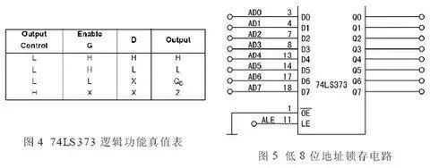
When the output is enabled (OE is L) and control enable (LE is H), the output follows the state; when OE is L and LE is L, the output holds the state.
The address latching circuit is shown in Figure 5. OE is grounded, and LE is connected to the ALE pin of the microcontroller, generating the low 8-bit address signal that meets the timing requirements.
Executing the following three instructions will yield the timing diagram shown in Figure 6.
MOV DPTR, # 0FF55H; Low 8-bit address is 55H
MOV A, # 0AAH; Data to be sent 0AAH → A (55H inverted)
MOVX, @DPTR, A; The data in A (0AAH) is sent to the object at address 0FF55H.
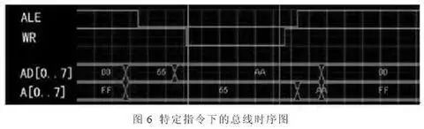
From Figure 6, it can be seen that the P0 port first sends 55H, and at the falling edge of ALE, address latching is achieved, followed by sending data 0AAH. During the effective period of WR (low level), the latch outputs the low 8-bit address 55H, while the P0 port sends out data 0AAH.
3. Complex Address Interface Circuit with Decoder
Theoretically, the high 8-bit address lines can produce 256 effective addresses. How can address “expansion” be achieved? Address expansion is accurately described as address decoding; for example, 3 address lines can decode into 8 addresses, and 4 lines decode into 16 effective addresses.Here, a 3-8 decoder is chosen to implement address decoding, with the circuit diagram and corresponding addressing shown in Table 1.
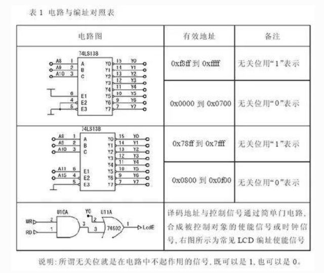
The microcontroller system for bus expansion interfaces includes external 32k RAM expansion, LCD1602 interface, and input/output ports.
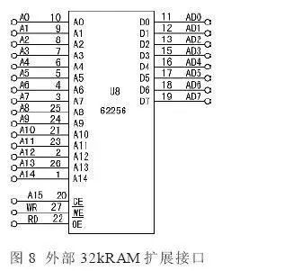
D0 to D7 connect to the data bus P0 port, and the address lines A0 to A14 connect to the low 15 bits of the microcontroller’s address bus. The microcontroller’s address line A15 connects to the RAM chip select signal, which is low-level effective. Thus, the RAM address allocation ranges from 0000H to 7FFFH, without conflict with the 74138 decoded addresses.
The LCD1602 interface circuit is shown in Figure 9.
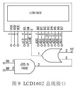
RS and RW are connected to A12 and A13, respectively, enabling signal addressing as Y7. Thus, the four driving addresses of the LCD (data read/write and command read/write) are from 0CFFFH to 0FFFFH (irrelevant bits are 1) or from 8700H to 0B700H (irrelevant bits are 0).
Sometimes, the microcontroller does not have enough pins and needs to be expanded. The input port expansion circuit is shown in Figure 10.
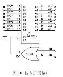
Using the high-impedance state function of 74HC573 (74LS373), its outputs Q0 to Q7 connect to the P0 port. During the bus address read operation, the input InPORT data can be read into the microcontroller’s accumulator, with addresses 0F8FFH or 8000H.
The output port expansion circuit is shown in Figure 11.
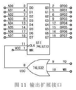
By using the data latching function of 74LS273, during the bus address write operation, data from the microcontroller’s accumulator can be written into the 273 latch output, with addresses 0F8FFH or 8000H. Since different control buses are used, the addresses can be shared with inputs.
Bus expansion is a crucial technology that must be mastered in designing microcontroller control circuits. Numerous special function ICs support bus interfaces, such as ADC0809, TLC7528, and DDS devices like AD9851.
The key point of bus interfaces is that under strict control timing, the bus is time-multiplexed to achieve complex system designs.
(Content sourced from the internet, copyright belongs to the original author)
Disclaimer: If there are copyright issues, please contact for removal! No individual or organization assumes related legal responsibilities.