This article is selected from the Jishu column “Arm Selection” by author lvy, authorized to be transferred from the WeChat public account Arm Selection. This article will take you deeper into the understanding of the MCU boot process.
I previously wrote an article analyzing the complete boot process of STM32, but I felt that some parts were not fully understood, so I made a summary of the unclear points.
1 Where does the MCU read code when it first starts?
After the CPU is powered on, it is designed to read code from address 0x00000000; it first reads two words consecutively, which are the initial value of the stack pointer and the address of the reset exception handler; then it jumps to execute the reset exception handler.
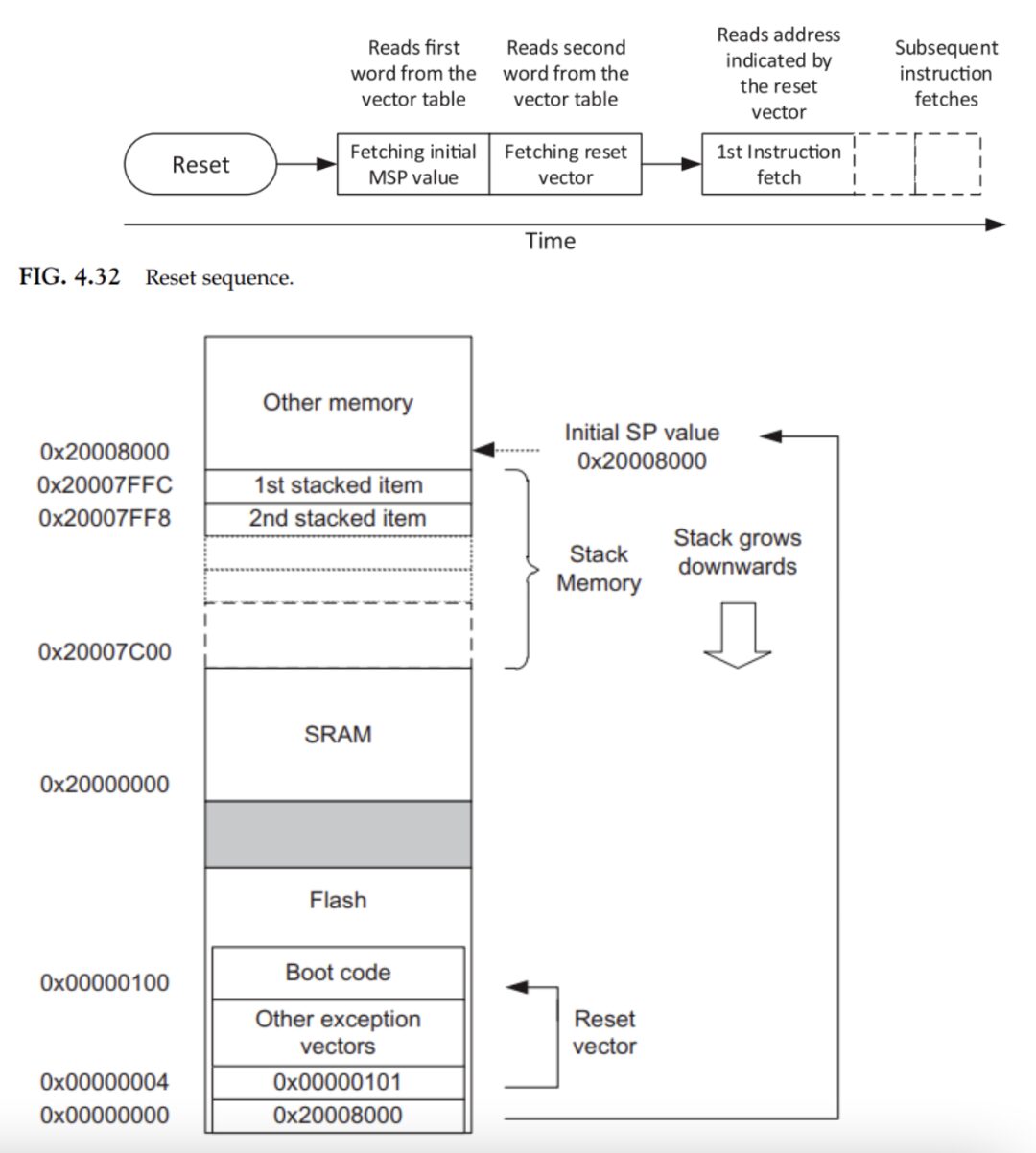
Figure 1
In some early Arm processor designs, such as the Arm7TDMI, the reset will directly read the code at address 0 for execution, where the software initializes the stack pointer, and the address 0 directly stores the interrupt handler function, not the function address.
Therefore, we can reasonably speculate that the first word is the stack address because the subsequent reset interrupt handler involves function jumps, which may already require storing content in the stack.
2 Is the code at address 0x0 bootROM code or user bootloader code?
The answer is both. It actually depends on where the user’s code is stored.
For some high-performance MCUs (such as the Cortex-A series), the code itself is relatively large and may be stored in an SD card or QSPI/SPI Flash. These MCUs must first execute code from bootROM because the storage of SD cards and SPI Flash is not in the MCU’s unified address space, and they cannot be accessed without initializing these peripherals. The bootROM Nor Flash can definitely be accessed directly by the MCU through the bus address, and the code at address 0 is located in the bootROM. After the code comes up from bootROM, it determines which peripheral to load the user program from through the boot pins and initializes the corresponding peripheral, transferring the user code stored in the peripheral to internal SRAM for execution. The subsequent boot process will not be elaborated.
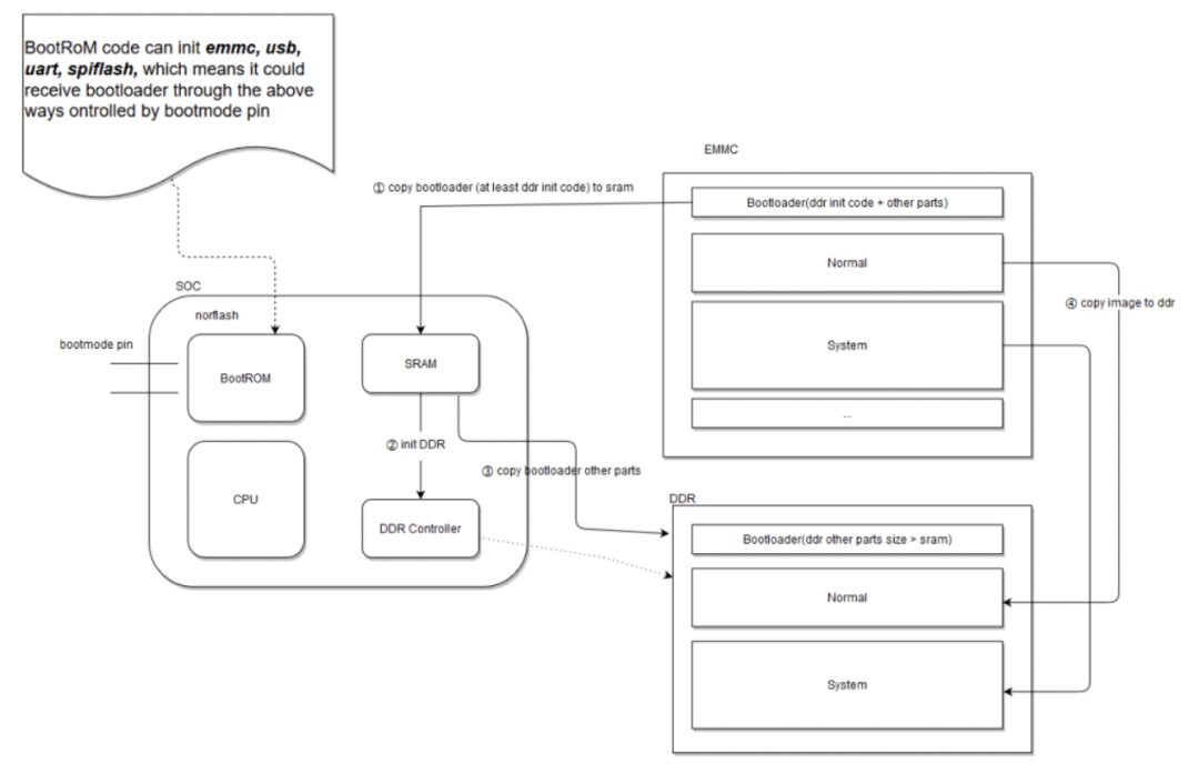
Figure 2
For some low-capacity MCUs, such as Cortex-M3/M4, they have built-in Flash in their chips, which is similar to the bootROM mentioned above, and can be accessed directly by the MCU through the address bus without needing to initialize external peripherals. Of course, these MCUs also have bootROM internally, so when these MCUs are powered on, they can choose to start from bootROM or from built-in Flash, which is selected through external pins. Whichever is selected will map its starting address to address 0.
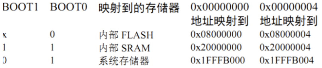
Figure 3
3 How do MCUs like Cortex-M3/M4 ensure that the Flash starting address is the stack pointer and the reset exception handler pointer?
This is actually determined by the compiled linker file. For example, below is an excerpt from my IAR linker file .icf.
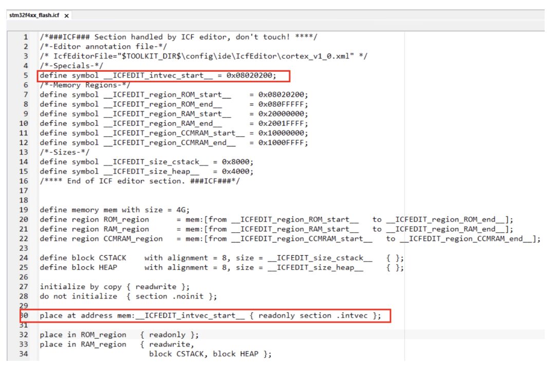
Figure 4
4 Is it possible for an MCU not to read code starting from address 0?
MCUs with the M7 core are more flexible and have changed the fixed reading of the interrupt vector table from address 0x0000 0000. Taking the STM32H7 as an example, it can boot from all addresses from 0x0000 0000 to 0x3FFF 0000. A special option byte is arranged for configuration.
Transferred from | Arm Technology Academy
Copyright belongs to the original author. If there is any infringement, please contact for deletion.
END


关于安芯教育


安芯教育是聚焦AIoT(人工智能+物联网)的创新教育平台,提供从中小学到高等院校的贯通式AIoT教育解决方案。
安芯教育依托Arm技术,开发了ASC(Arm智能互联)课程及人才培养体系。已广泛应用于高等院校产学研合作及中小学STEM教育,致力于为学校和企业培养适应时代需求的智能互联领域人才。