Understanding Display Technologies: LCD, OLED, Mini/Micro LED

Understanding Display Technologies: LCD, OLED, Mini/Micro LED
Liquid Crystal Display (LCD) technology is essentially the most mainstream human-computer interaction interface today. Despite the emergence of new technologies, such as the latest Mini LED, they still fall under the LCD category. How do we practically distinguish them, and how do they differ from older technologies?
Liquid crystal refers to the liquid crystal phase, which possesses unique physical and optical properties. It is widely used in display technology and significantly improves the thinness of devices, making it the most common display technology today. Essentially, all widely discussed liquid crystal screens belong to the LCD (Liquid-crystal Display) category. However, what is currently referred to as LCD in the market specifically denotes active matrix TFT-LCD technology, while passive matrix STN LCD technology has been phased out.
TFT-LCD, or Thin Film Transistor Liquid Crystal Display, means that each liquid crystal pixel on the display is driven by integrated thin film transistors, which independently control the pixels, improving response speed and allowing precise control of color levels. This technology is the foundation of current consumer products, as it is not only well-developed but also cost-effective.

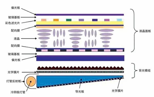
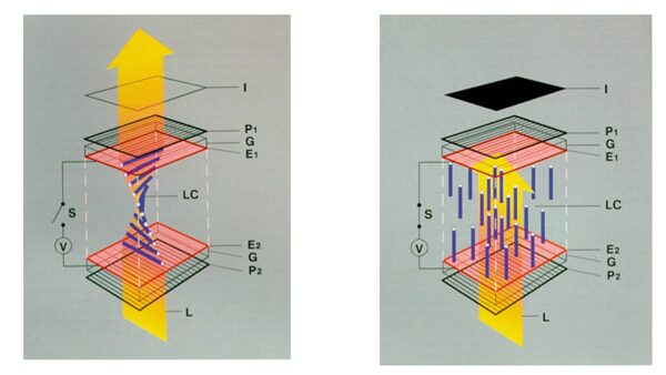
Types of Liquid Crystals

Understanding Display Technologies: LCD, OLED, Mini/Micro LED
LCD panel structure (Source: I, Wasami007 / CC BY-SA)
The main working principle of TFT-LCD is that a layer of liquid crystal is sandwiched between two glass substrates. The upper glass substrate contains color filters, while the lower glass substrate is embedded with transistors. When current flows through the transistors, the resulting electric field causes the liquid crystal molecules to tilt, changing the light. Voltage determines the brightness of each pixel, with each pixel containing red, green, and blue to form the image output. Although its circuit layout is similar to DRAM, it is constructed on glass, and its process primarily involves creating an amorphous silicon layer or polysilicon layer rather than high-end transistors that require epitaxy.
Based on this technology, products with quality and cost differentiation have been developed. Currently, there are three main types: TN, VA, and IPS panels, differing mainly in their liquid crystal layers. Twisted Nematic liquid crystals (TN) are the lowest-cost LCD panel type, yet their pixel response is fast enough to meet most needs. Samsung has further developed the B-TN technology for even faster response and richer colors.
Understanding Display Technologies: LCD, OLED, Mini/Micro LED
The left image shows the off state where light can pass through TN liquid crystal; the right image shows the state with voltage applied where light cannot pass through.
(Source: illustration by courtesy of M. Schadt. (based on copyright claims). / CC BY-SA)
However, the viewing angle of TN liquid crystals is a significant issue. VA liquid crystal panels offer a further solution, achieving nearly 170° viewing angles without special compensation films. This is due to the use of vertically aligned liquid crystals, which achieve higher contrast but are slower and more expensive, categorizing them as mid-range products.
The highest-end TFT-LCD is IPS, which employs In-Plane Switching technology to effectively improve viewing angle issues and various traditional TN panel problems. It has excellent viewing angles and consumes less power than VA panels, making it ideal for touch screens. Early iPhones and iPads used IPS liquid crystals, but they are also more expensive.
Due to the rapid development of TFT-LCD manufacturing processes, before the emergence of new LED technologies, discussions about panels mainly revolved around these three categories. Other new types, such as Samsung’s PLS, PVA panels, and Fujitsu’s MVA panels, have emerged, but they mainly maintain performance while striving to lower costs. Consequently, traditional narrow-view TN panels are gradually being phased out.

Success Lies in Open Cell

Although currently in a red ocean, the panel industry once thrived in Taiwan. The main components of TFT-LCD panels include glass substrates, backlight modules, polarizers, color filters, and optical films. Taiwanese manufacturers are involved in the entire supply chain, but well-known companies like AUO and Innolux primarily produce Open Cell and module assembly.
The Open Cell process of TFT-LCD generally consists of three stages: front, middle, and back. The front stage refers to the production of TFT glass, which is similar to semiconductor processes, involving coating and etching to embed thin film transistors on the glass substrate. The middle stage involves bonding the TFT glass with color filters and adding polarizers, while the back stage combines the driver IC and printed circuit board to complete the so-called Open Cell, which is only a semi-finished product.
Understanding Display Technologies: LCD, OLED, Mini/Micro LED
Front stage Array similar to semiconductor, TFT glass process. (Source: Innolux)
It is worth mentioning that although a backlight module is necessary for use, many terminal manufacturers choose to purchase Open Cell directly to integrate panel and product packaging, allowing for more design flexibility. This is particularly popular among mainland TV assembly plants, which account for over half of global production capacity, adopting the BMS model (Backlight Module System). Several years ago, companies like AUO and Innolux began shifting towards shipping Open Cell. While shipping Open Cell indeed yields higher profits than modules, it saves panel manufacturers considerable material management costs. However, this is a double-edged sword.
If panel manufacturers focus solely on producing semi-finished products, their high degree of standardization makes it difficult to develop product combinations tailored to different functional needs, leading to an oversupply situation and ultimately losing market voice. Some studies suggest that the shift towards Open Cell shipping methods has led to rapid price declines, which is detrimental to the capital-intensive panel industry in the long run, and is one reason why mainland manufacturers easily surpassed established giants through price subsidies.
Of course, display technology is not limited to LCD. In recent years, Organic Light-Emitting Diode (OLED) technology has emerged, regarded as the new mainstream despite its pros and cons.
Essentially, the working principles of LCD and OLED are entirely different. OLED has self-emitting characteristics, requiring no backlight and color filters, resulting in a thinner structure, making it favored by the industry. Like LED, OLED also utilizes the recombination of electrons and holes between the conduction band and valence band to emit energy in the form of light. However, in terms of materials, it uses polymer organic films, eliminating the need for complex epitaxy processes, and achieving higher efficiency in light emission.
These numerous characteristics have led to high expectations for OLED in the industry, and it has been widely adopted. Since 2018, when Apple’s iPhone products began using OLED screens, the technology has gradually gained popularity. Compared to LCD, OLED has significant advantages in viewing angles, contrast, color gamut, and brightness, but due to cost and technical issues, OLED still struggles to compete with LCD in large-size products.

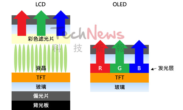
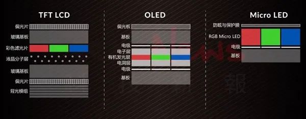
Differences Between OLED and LCD

The basic structure of OLED consists of a layer of organic light-emitting material fabricated on indium tin oxide (ITO) glass, covered with a layer of low work function metal electrodes. When driven by external voltage, holes from the anode and electrons from the cathode combine in the light-emitting layer, releasing photons that produce red, green, and blue primary colors, forming the basic color palette.
Understanding Display Technologies: LCD, OLED, Mini/Micro LED
The biggest difference between OLED and LCD is self-emission. (Source: Technology News)
To enhance the injection and transport capabilities of electrons and holes, a hole transport layer is typically added between the ITO and the light-emitting layer, and an electron transport layer is added between the light-emitting layer and the metal electrodes to improve light-emitting performance. In fact, the commonly mentioned active matrix OLED (AM-OLED) also utilizes thin film transistors, similar to TFT-LCD, emitting light based on the instructions received by the transistors. Another difference is that AM-OLED commonly uses circular polarizers to reduce display interference instead of linear polarizers.
There are also passive matrix OLED (PM-OLED), but they have significant drawbacks. The most criticized aspect of OLED screens is the limited lifespan of pixel points due to material constraints, leading to issues like color fading and burn-in over time. PM-OLED operates under high pulse currents, resulting in even shorter pixel lifespans and limited resolution, making it suitable only for small-sized products. Consequently, despite lower costs, PM-OLED is less favored, with the market showing a higher acceptance of AM-OLED.
OLED manufacturing processes are also divided into front, middle, and back stages, with the main difference from LCD being the Cell process, primarily using vacuum deposition methods. Under high vacuum conditions, organic materials are vaporized through heating and deposited onto the substrate surface through fine metal masks (FMM), forming RGB pixel points. The high purity of the materials produced in this way leads to longer device lifespans, making it the mainstream method. However, the high precision required for this process prevents the originally simple OLED panel structure from reducing costs.
Understanding Display Technologies: LCD, OLED, Mini/Micro LED
OLED panel main manufacturing processes. (Source: Technology News)

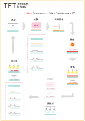
Semiconductors and the Panel Industry

Returning to the similarities between the panel and semiconductor industries, both involve processes and large-scale capital expenditures, leading many to associate the panel industry with semiconductors. However, there are significant differences, particularly in the degree of product standardization. Semiconductor chip designs vary widely to accommodate different functions, but panels have relatively less differentiation. In this context, capacity and cost control become the primary objectives, as previously mentioned with the shift towards Open Cell in the panel industry.
Regardless of the pros or cons, vertical integration (IDM) may be a more suitable model for the panel industry, potentially leading to larger companies dominating the market. Building capacity is not easy, as key equipment like OLED deposition machines are difficult to acquire, creating barriers. This has led to the current situation where OLED is mainly dominated by Korean manufacturers, with Samsung holding nearly 90% of the market.
Currently, industry newcomers are actively pursuing lower-cost inkjet printing processes. Recently, domestic giants like BOE have been seen as potential challengers to Samsung, primarily due to their prospects for mass-producing inkjet-printed OLEDs. OLED screens are currently the preferred choice for small smart mobile devices, outperforming LCD in performance, especially with flexible substrates being essential in emerging foldable applications. However, it will take the realization of inkjet printing processes before OLED can potentially dominate the large-size market and become the true mainstream technology.

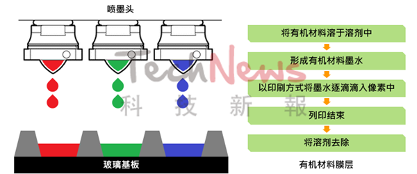
Challenges of Inkjet Printing

Using deposition processes, large-size panels are prone to warping and precision metal shielding issues, leading to defects. However, inkjet printing can overcome these challenges at a lower cost, as it does not require a vacuum environment or FMM, and has higher material utilization, making it more suitable for large-scale production. Nevertheless, this does not mean it is easier; inkjet printing mainly involves using solvents to dissolve OLED organic materials and directly spraying them onto the substrate surface to form pixels. Developing usable cathode inks and achieving uniform film formation over large areas are significant technical challenges.
Understanding Display Technologies: LCD, OLED, Mini/Micro LED
RGB organic inkjet printing technology. (Source: Technology News)
Additionally, to produce high-resolution panels comparable to those made by deposition methods, precise control of the inkjet head positioning and droplet volume is crucial. This requires not only a mechanical platform capable of very precise operations but also optimizing the chemical composition of the ink to better control evaporation and film formation processes. Furthermore, the substrate structure design must meet specific requirements to ensure the ink spreads and wets the surface perfectly. All these aspects require equipment and processes to meet certain standards.
Nonetheless, inkjet printing processes present an opportunity for domestic manufacturers to achieve a leapfrog advantage, bypassing the barriers set by Korean manufacturers in equipment and materials. Domestic companies like Tianma and Huaxing have collaborated to establish Guangdong Juhua to better realize this technology. Of course, Samsung will not sit idly by as competitors catch up; in recent years, it has also actively invested in inkjet printing processes and patent layouts. If it manages to apply this technology to its QD-OLED panels first, Samsung’s market position may become even more unshakeable.
In recent years, quantum dot display technology has become a trend, but it is fundamentally unrelated to OLED and LCD, while Mini LED and Micro LED are not just size differences. Finally, let’s briefly introduce how these emerging technologies are distinguished.
Quantum dots are semiconductor nanostructures that can confine excitons in three spatial directions, with the emission frequency varying based on the size of the semiconductor. This means that by adjusting the size of these nanostructures, one can control the emitted color, which has high optical stability.
Based on these properties, theoretically, this fluorescent material can produce a continuous spectrum effect close to natural light, with a wide color gamut and longer lifespan, showing potential to become the ultimate display technology. In simple terms, this is a technology that can optimize light sources without the burn-in issues of OLED. Quantum dot technology was initially applied to LCDs and other non-self-emitting displays before research on its application in OLED began. Currently, the two are typically distinguished as QLED and QD-OLED.

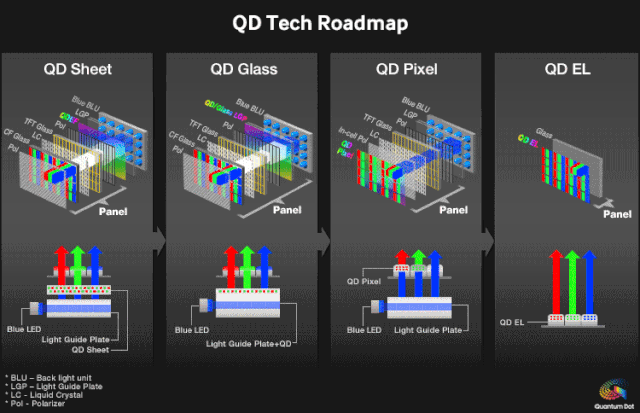
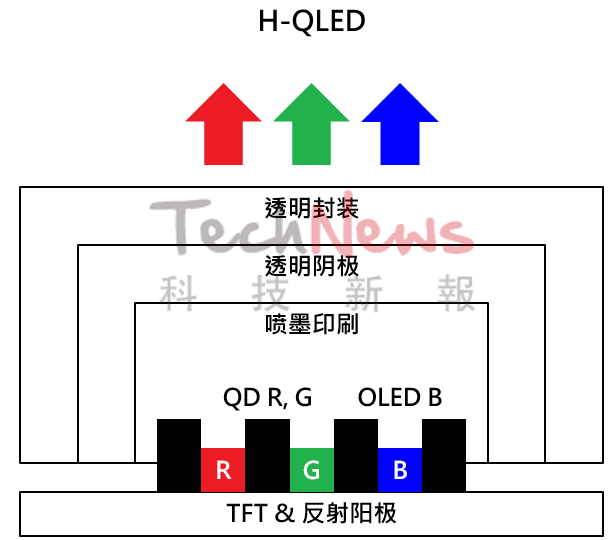
Positive Development, Difficult Mass Production

While QLED, like LCD, relies on backlighting and inherits its drawbacks, it can emit purer colors through quantum dot films (QDEF). Samsung’s recent development of QD-OLED takes it a step further, using blue OLED light sources to excite quantum dots of different sizes to produce red and green light. This not only enhances performance but theoretically lowers costs compared to the original WOLED technology. Coupled with inkjet printing processes, it is expected to maintain market dominance. However, as of now, Samsung’s ideal QD-OLED technology has low light conversion rates, and despite recent optimistic news, overall commercial readiness remains insufficient.
Understanding Display Technologies: LCD, OLED, Mini/Micro LED
The ideal quantum dot display technology is the electroluminescence (EL) shown on the far right, which no longer requires color conversion and has not yet been clearly named. (Source: Samsung Display)
In fact, manufacturing quantum dots is not easy; the material structure must be reduced to below 100 nanometers, imposing higher requirements on the process. The materials that can be used are still limited. Although the first quantum dot technology display appeared in 2006, quantum dot materials are often sensitive to heat, making mass production using vacuum deposition methods challenging. This necessitates reliance on advancements in inkjet printing. Therefore, the quantum dot TVs seen on the market today are essentially QLEDs similar to LCDs, not QD-OLEDs. Currently, Samsung’s more mature technology is inorganic material inkjet printing.
Meanwhile, there have been significant advances in mainland China. At CES 2019, Huaxing Optoelectronics also released a hybrid OLED and QLED technology called H-QLED, utilizing inkjet printing. In CES 2020, they showcased flexible OLED inkjet-printed panels and recently invested in Japan’s JOLED, potentially acquiring related technology, although there have been no mass production announcements for these products yet.
Understanding Display Technologies: LCD, OLED, Mini/Micro LED
Comparing the technology roadmaps of Samsung, H-QLED is still a technology similar to QD-OLED. (Source: Technology News)
According to analysts at TrendForce, overcoming the bottlenecks of emerging display technologies is challenging. QD-OLED may not be available until 2021, and even though mainland China has begun laying out production lines for OLED inkjet printing technology, issues such as low PPI remain, making true maturity more likely after 2022.

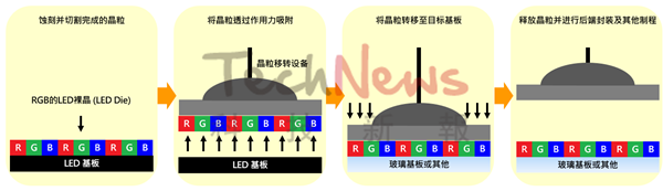
The Ambiguity of Mini LED and Micro LED

However, the most discussed topics currently may not be quantum dot technology, but Micro LED and Mini LED, which are also considered advanced display technologies. Micro LED refers to “micro light-emitting diodes”, while Mini LED is formally named “sub-millimeter light-emitting diodes”, with the size distinction generally set at 100 microns, about 0.1 millimeters. However, Micro LED prototypes have already been developed below 3 microns, and the technical challenges do not lie in producing miniaturized chips.
In fact, there was initially no distinction between Mini and Micro; manufacturers created differentiation to compete, resulting in increasingly varied definitions. In recent years, there has even been talk of Nano LED, but Micro LED is regarded as the ultimate technology, as true nanoscale devices are difficult to emit light. However, it is worth noting that RGB Mini LED is not just used for backlighting but also for direct display. Although it competes with OLED in terms of wide color gamut and vibrancy, the costs remain astonishingly high, making it still a niche market.
Understanding Display Technologies: LCD, OLED, Mini/Micro LED
Comparison of the structures of the three major display technologies. (Source: Technology News)
Overall, Mini LED is still regarded as a transition to Micro LED. Mini LED is mostly used in traditional LCD structures, shrinking the backlight LEDs. Micro LED aims to directly package light-emitting components, achieving independent driving of inorganic self-emission, even outperforming OLED, and is hailed as a new blue ocean by the industry. While the process has been simplified, the technology is more challenging, particularly the mass transfer technology that will directly affect the design cycle of Mini LED and the mass production opportunities of Micro LED.
Understanding Display Technologies: LCD, OLED, Mini/Micro LED
The concept flow of mass transfer technology. (Source: Technology News)
Therefore, Taiwanese manufacturers are more actively developing Mini LED, while Samsung, which plans to exit the LCD market, is focusing directly on Micro LED. In simple terms, the main difference between Mini or Micro LED technology and the previously discussed technologies lies in the later processing stages, where mass transfer, packaging testing, and even maintenance present significant challenges. Additionally, with technological advancements, the definition of Mini LED may continue to shrink, with sizes over 50 microns potentially still being classified as Mini LED in the future.
Lastly, it is worth noting that the Mini LED referred to by Taiwanese manufacturers differs conceptually from the Mini LED displays commonly discussed in mainland China. The Taiwanese definition indeed refers to miniaturized chip sizes, while the mainland emphasizes packaging methods. For Mini LED backlight modules, denser chip arrangements can create ultra-thin light sources. In self-emitting displays, Mini LED can also achieve smaller pixel pitch packaging, resulting in certain product differentiation.
Source: TechNews
Understanding Display Technologies: LCD, OLED, Mini/Micro LED
For more in-depth information on Mini LED, click to learn about LEDinside’s “2020 MiniLED Next-Generation Display Technology and Supply Chain Analysis”.
Understanding Display Technologies: LCD, OLED, Mini/Micro LED
Read more about the latest news on Mini LED here

Leave a Comment

×