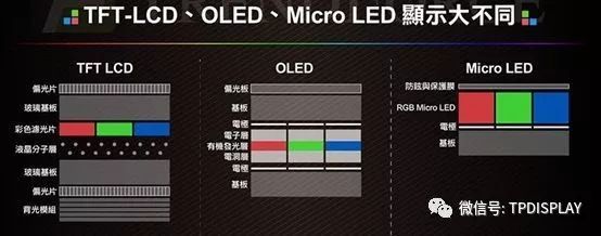
LCD (Liquid Crystal Display): Backlight source emits light + liquid crystal color rendering, with the backlight source now using LED lights.
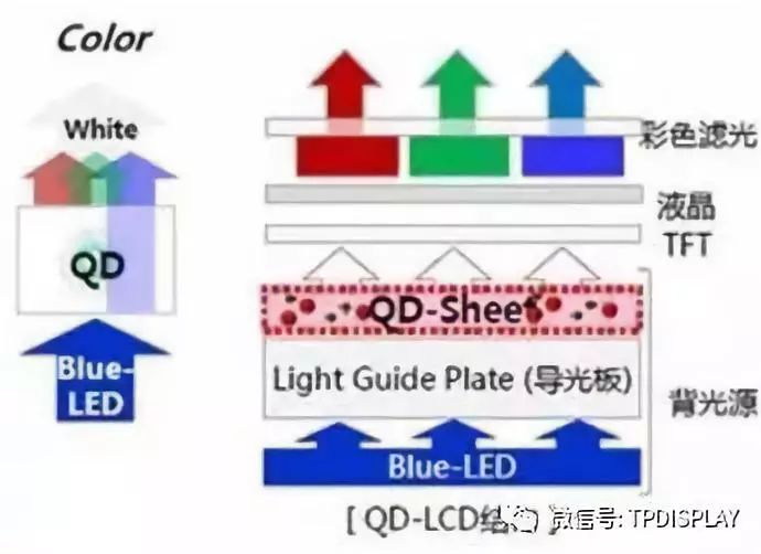
QD-LCD (Quantum Dot TV): The screen of a typical LCD TV uses an LED backlight that emits blue light, which is converted into red, green, and blue light through phosphors, ultimately forming white light, which is then projected onto the liquid crystal for color rendering. QD-LCD replaces phosphors with quantum dots, allowing the blue light emitted by LEDs to hit the quantum dot film, resulting in better color gamut and brightness for red and green light, which is then combined with blue light to render colors on the liquid crystal, leading to superior display performance.
Mini-LED: A technology that enhances the backlight of existing LCD display technology by using smaller LED lights as the backlight source, allowing for more precise control of the image. Currently, edge-lit backlight designs require only a few dozen high-brightness LEDs, while miniLED requires tens of thousands of small LEDs.
LED: Emits light and renders colors when powered on, with the light-emitting materials being GaAs (Gallium Arsenide), GaP (Gallium Phosphide), and GaAsP (Gallium Arsenide Phosphide) semiconductors.
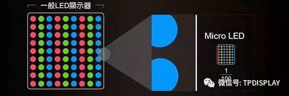
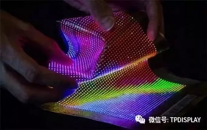
MicroLED: MicroLEDs are very small light-emitting diodes, with LED units smaller than 100 microns. Each light-emitting diode contains red, green, and blue sub-pixels. MicroLED technology uses inorganic materials to achieve light emission. While traditional LEDs can only be made into large screens for stadiums and shopping malls, MicroLEDs can be made small enough for TVs and watches. In early January of this year, Samsung Electronics unveiled the world’s first 146-inch modular “The Wall” TV, which uses MicroLED technology and is said to be available for sale in August.
OLED: Emits light and renders colors when powered on, with the light-emitting and color-rendering materials being organic molecular polymers.
QLED: Emits light and renders colors when powered on, with the light-emitting materials being quantum dots, which are inorganic semiconductor nanocrystals typically composed of zinc, cadmium, selenium, and sulfur atoms.
1. LCD (Liquid Crystal Display) is short for Liquid Crystal Display. The structure of an LCD involves placing liquid crystals between two parallel glass plates, with many vertical and horizontal fine wires in between. By controlling the electric field through the application of voltage, the orientation of the rod-shaped crystal molecules is altered, refracting light to produce an image.
LCDs do not emit light by themselves and require a backlight. They are composed of a TFT substrate and a CF (color film) substrate, with liquid crystals filled in between. The TFT substrate provides an electric field to control the angle of rotation of the liquid crystals, thereby controlling the liquid crystal’s transmittance. The color film is printed with RGB color blocks, and the light from the backlight passes through the transparent TFT substrate, through the liquid crystal molecules, and then through the CF substrate. The varying transmittance of the liquid crystal molecules under each color block results in different brightness levels of red, green, and blue, which can be mixed to display the desired color.
2. What does LED mean? LED = Light Emitting Diode, a solid-state semiconductor device that can convert electrical energy into visible light. It can directly convert electricity into light. LED applications can be divided into two main categories: one is LED displays; the other is LED single-tube applications, including backlight LEDs, infrared LEDs, etc. LED displays are composed of an array of light-emitting diodes and use low-voltage scanning drive technology, featuring low power consumption, long lifespan, low cost, high brightness, low failure rate, wide viewing angles, and long visibility distance.
3. OLED stands for Organic Light Emitting Diode, which is a self-emitting device that does not require a backlight. It emits light and renders colors by itself, making it a replacement for LCDs. Its structure consists of an RGB organic film layer that can emit light when powered on, deposited on a TFT substrate. By controlling the current through the TFT substrate, the brightness of the RGB organic film layer can be controlled, thus mixing to produce the desired display color.
4. Mini-LED:
In flat panel displays, Mini-LED refers to sub-millimeter light-emitting diodes. Mini LED technology transforms the few dozen LED beads used in edge-lit backlighting into thousands or tens of thousands of direct backlight sources. It is estimated that a 55-inch TV’s backlight unit (BLU) requires about 40,000 mini LEDs, while a smartphone panel requires about 9,000.
Mini-LED technology is an enhancement to existing LCD display technology’s backlight, significantly improving the color performance and contrast of display panels, but it also greatly increases the cost of the display panel. Currently, there are no mass-produced mini-LED products on the market, but reports suggest that mass production may be available in 2018.
5. QD-LCD:
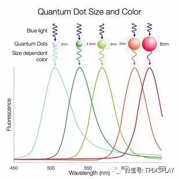
Quantum dots are inorganic semiconductor nanocrystals typically composed of zinc, cadmium, selenium, and sulfur atoms, structured in three layers: core, shell, and ligand. When stimulated by light or electricity, quantum dots emit light, with the color of the light determined by the materials and size of the quantum dots. Ideally, by controlling the continuous variation of the quantum dot material’s diameter, a continuous spectrum effect close to natural light can be achieved.
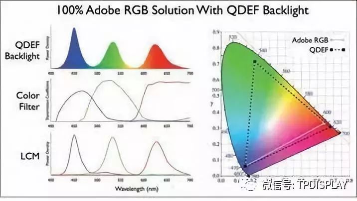
QD-LCD refers to the application of quantum dot films in traditional LCD screens, using quantum dot technology to replace the yellow phosphors in blue LED optical packaging materials to enhance color gamut and brightness. The light emitted by the blue LED backlight is transformed into red and green light through the quantum dot film, achieving full-color display. QD-LCD technology is an improvement to LCD display technology, fundamentally still relying on LCD technology under backlight. Quantum dot films developed by 3M and Nanosys have already been applied in the LCD display field, enabling full-color display.
The greatest advantage of quantum dot films is their high reliability, which can be compatible with traditional LCD backlight structures, allowing for the transformation of display panels simply by replacing the white light source in LCDs with blue LEDs. The biggest advantage of QD-LCD technology is that it can fully utilize the production lines of TFT-LCDs, reducing production costs.
6. Micro-LED:
In simple terms, Micro-LED is a miniature version of outdoor LED billboards, integrating individual LED lights onto semiconductor chips to form a high-density array of tiny LEDs, with each MicroLED acting as a pixel that can be individually driven. The pixel distance is on the micrometer scale.
Since Micro LED is a self-emitting technology, its advantages include low power consumption, high brightness, ultra-high resolution and color saturation, fast response speed, energy efficiency, long lifespan, etc., with power consumption about 10% of LCDs and 50% of OLEDs. Structurally, Micro-LED is much simpler than TFT-LCD and OLED.
In terms of production technology, Micro LED Display combines the characteristics of both TFT-LCD and LED technologies, with mature developments in materials, processes, and equipment, but several key production steps still need breakthroughs.
Due to the high specifications of Micro-LED technology products compared to current TFT-LCD or OLED, major companies like Apple are vigorously researching this technology and its products.
7. QLED: A technology evolved from quantum dot and LED technology.
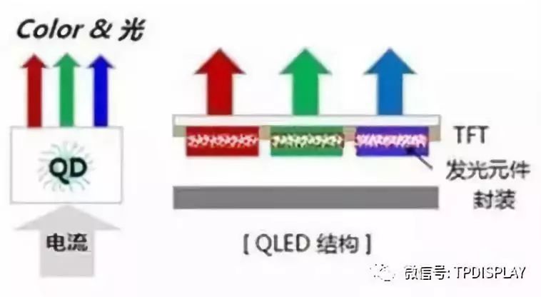
QLED technology is based on the electroluminescent properties of quantum dots, utilizing the self-emission of quantum dots under electrical drive as the basis for display, with the quantum dot material itself serving as the light-emitting material to achieve image display. Its structure is very similar to OLED technology, with the main difference being that the light-emitting center of QLED is made of quantum dot materials. QLED technology has advantages such as strong contrast, energy efficiency, wide viewing angles, and high color saturation, making products thinner and lighter, representing a promising display technology. However, due to limitations in related materials and process development, QLED is still in the laboratory research stage.
Basic Processes and Future Directions of OLED Technology
ITO panel [Array manufacturing process] → ITO panel (forming organic film) → OLED module packaging testing → OLED finished product. Due to the simple structure of OLED, its production process is not as complex as that of TFT-LCD manufacturing. The production process involves organic materials, ITO panels (Array manufacturing process), ITO panels (forming organic film), and OLED module packaging testing.
In the Array manufacturing process, the cleanliness of the ITO panel is a key factor in OLED quality. Thus, the cleaning method of the panel has become a commercial secret for various manufacturers. The molecular structure of OLED affects the integrity of the film formation; if the film is uneven, it will cause uneven light emission. Therefore, the appropriate selection of organic materials naturally becomes a focus of research and development and future competitive advantage for manufacturers.
Additionally, during the thin film formation process, the generation of by-products can produce impurities that affect light emission efficiency and product lifespan, making moderate purification necessary in the manufacturing process. Furthermore, OLED device materials are susceptible to moisture and oxygen, which can degrade the device and affect its lifespan. Therefore, during the packaging process after coating, it is essential to eliminate moisture from the air. The success of packaging technology directly impacts the success of the device, making packaging technology a crucial part of the entire manufacturing process. Currently, there is no optimal packaging method, and although the OLED production process is relatively simple, various manufacturing stages still face different challenges that need to be overcome. Therefore, there is currently no standard mass production technology for OLEDs, and manufacturers still have considerable room for development in manufacturing processes.
OLED also has a complex background.
When discussing OLED, we must mention the term EL, which stands for electroluminescence, one of the most common light-emitting methods. OLED belongs to “organic EL,” while “inorganic EL” is also a category. In Japan, OLED is often referred to as “organic EL,” which is not incorrect from a classification perspective. Organic EL also has different types, with the most common being small molecule OLEDs and high molecular weight PLED light-emitting technology.
EL (Electro-Luminescence) displays refer to displays that achieve light emission by applying current to light-emitting materials, with a light emission principle similar to that of light-emitting diodes (LEDs).
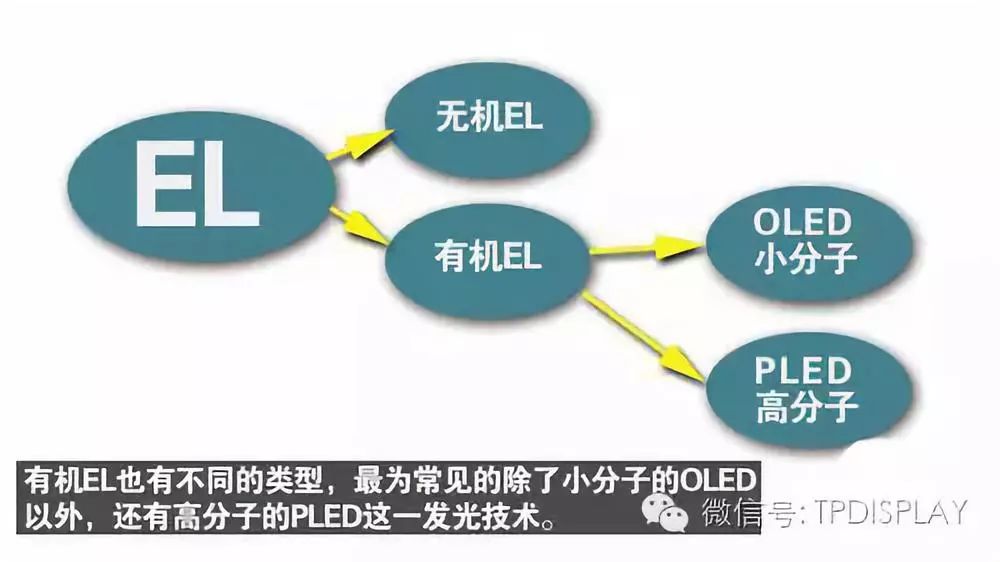
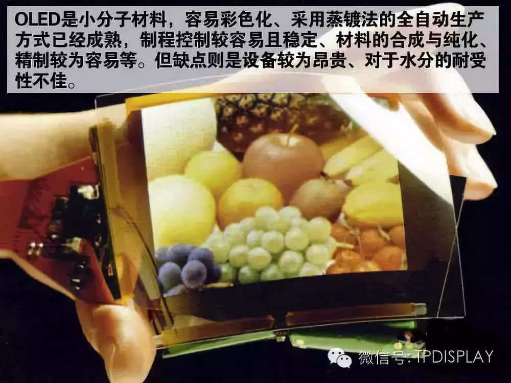
OLED (Organic Light Emitting Diode) and PLED (Polymer Light Emitting Diode) have similar chemical structures and light emission efficiencies, with the difference being the molecular weight. OLED uses small molecular materials, which are easier to colorize, and the fully automated production method using vapor deposition is mature, with process control being relatively easy and stable, and material synthesis and purification being relatively straightforward. However, the disadvantages include high equipment costs, poor moisture resistance, low vapor deposition rates, and material waste.
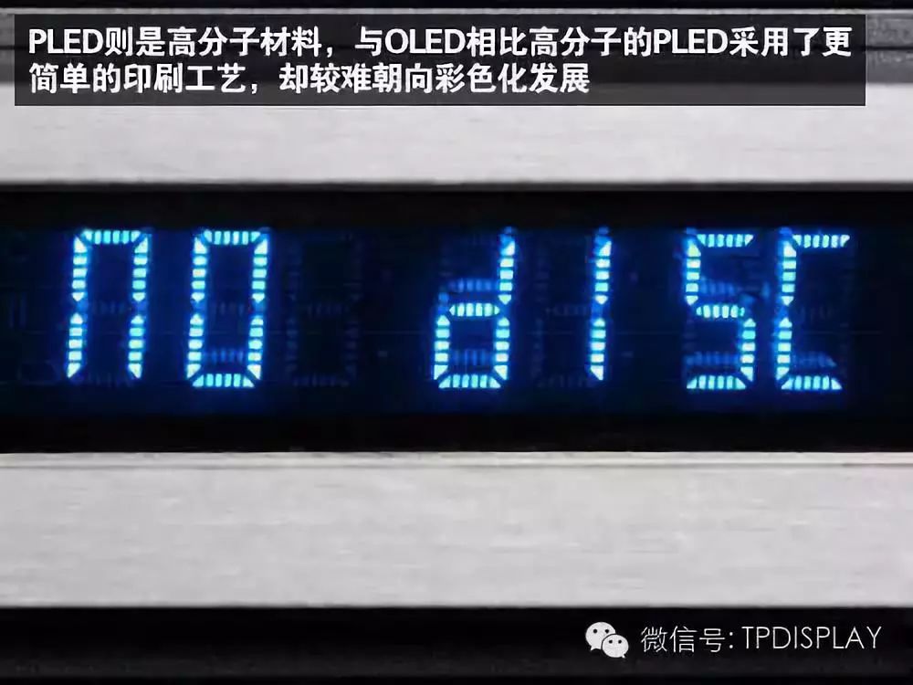
PLED, on the other hand, uses high molecular materials and employs a simpler printing process compared to OLED, rather than vapor depositing multiple layers of organic films. It is also more resistant to heat and cold. However, due to the different attenuation constants of each color in PLED, compensation is necessary, making it difficult to develop color displays, which is why we rarely see colored PLED screens.
1. Pre-treatment of Indium Tin Oxide (ITO) Substrate
1. ITO surface flatness: ITO is widely used in the manufacturing of commercial display panels due to its high transmittance, low resistivity, and high work function. Generally, ITO manufactured using RF sputtering is prone to surface irregularities due to poor process control, leading to surface protrusions or spikes. Additionally, high-temperature sintering and recrystallization processes can create surface protrusions of about 10 to 30 nm. These irregular layers can provide pathways for holes to directly reach the cathode, increasing leakage current. There are generally three methods to address the impact of this surface layer: one is to increase the thickness of the hole injection layer and hole transport layer to reduce leakage current, commonly used in PLEDs and OLEDs with thicker hole layers (~200nm). The second is to reprocess the ITO glass to smooth the surface. The third is to use other coating methods to achieve better surface flatness.
2. Increasing the work function of ITO: When holes are injected from ITO into HIL, a large potential difference can create a Schottky barrier, making it difficult for holes to be injected. Therefore, reducing the potential difference at the ITO/HIL interface becomes a key focus of ITO pre-treatment. Generally, we use O2-Plasma treatment to increase the saturation of oxygen atoms in ITO, thereby increasing the work function. After O2-Plasma treatment, the work function of ITO can be increased from 4.8 eV to 5.2 eV, which is very close to the work function of HIL.
Adding auxiliary electrodes: Since OLEDs are current-driven components, long or thin external circuits can create significant voltage gradients, causing the voltage across the OLED component to drop, reducing the panel’s brightness. Due to the high resistance of ITO (10 ohm/square), unnecessary external power consumption can occur. Adding an auxiliary electrode to reduce the voltage gradient has become a quick way to increase light emission efficiency and reduce driving voltage. Chromium (Cr) is the most commonly used material for auxiliary electrodes due to its stability against environmental factors and high selectivity against etching solutions. However, its resistance value at a thickness of 100 nm is 2 ohm/square, which is still too high for some applications. Therefore, aluminum (Al), which has a lower resistance value (0.2 ohm/square) at the same thickness, has become another better choice for auxiliary electrodes. However, the high reactivity of aluminum raises reliability concerns, leading to proposals for multi-layer auxiliary metals, such as Cr/Al/Cr or Mo/Al/Mo. However, this increases complexity and cost, making the choice of auxiliary electrode materials one of the key points in OLED processes.
2. Cathode Process
In high-resolution OLED panels, isolating the fine cathodes is typically done using a mushroom structure approach, similar to the negative photoresist development technique in printing technology. During the negative photoresist development process, many process variation factors can affect the quality and yield of the cathodes, such as bulk resistivity, dielectric constant, high resolution, high Tg, low critical dimension (CD) loss, and appropriate adhesion interfaces with ITO or other organic layers.
3. Packaging
1. Moisture-absorbing materials: The lifespan of OLEDs is easily affected by surrounding moisture and oxygen. Moisture sources can be divided into two types: one is external environmental penetration into the component, and the other is moisture absorbed by each layer of material during the OLED process. To reduce moisture entering the component or eliminate moisture adsorbed during the process, the most commonly used material is desiccant. Desiccants can capture freely moving water molecules through chemical or physical adsorption to remove moisture from within the component.
2. Process and Equipment Development: The packaging process flow is shown in Figure 4. To place the desiccant between the cover plate and successfully bond the cover plate to the substrate, it must be done in a vacuum environment or by filling the chamber with inert gas, such as nitrogen. It is important to note that how to make the connection between the cover plate and substrate more efficient, reduce packaging process costs, and minimize packaging time to achieve optimal mass production rates has become one of the three main goals of packaging process and equipment technology development.
Efforts to Improve OLED Production Efficiency
The process of forming a uniform thin film layer of organic materials on the glass substrate is a key factor in producing OLED TVs. Currently, vacuum thermal evaporation (VTE) is the most widely used technology. The process using this technology must be conducted in a vacuum chamber, requiring a light-blocking plate to be placed close to the glass substrate to determine the pattern of deposited materials on the substrate. However, vacuum thermal evaporation technology has some drawbacks in producing large-screen OLED TVs. For example, the light-blocking plate is easily affected by the high-temperature environment during the process, causing it to shift, making it difficult to maintain a uniform deposition rate on large substrates.
Inkjet printing technology can form thin film layers through the uniform deposition of liquid organic materials. Therefore, this technology theoretically better addresses the size issues of large displays. Epson has adopted an on-demand inkjet process similar to that of inkjet printers, allowing for precise deposition of organic materials in the desired locations. Due to the high material utilization rate of inkjet systems, manufacturers can reduce production costs. Additionally, when applied to OLED TV production processes, the absence of a light-blocking plate reduces the number of process steps compared to vacuum thermal evaporation technology, making inkjet technology promising for significantly increasing yield.
OLED display technology is a comprehensive technology that integrates multiple fields and disciplines, covering semiconductors, organic chemistry, inorganic chemistry, thin-film electronics, vacuum physics, optics, etc. The key technologies involved mainly include TFT technology, colorization technology, organic film formation technology, and device packaging technology, each of which has various technical routes, with each route having its advantages and disadvantages. This complexity is both a challenge and a charm of OLED technology, making it a hot topic that industry players are eager to discuss.
Four Distinct Technical Routes
AMOLED has higher requirements for TFT technology than LCD, and the reason for this difference lies in the fact that AMOLED is a current-driven device.
TFT technology has been maturely applied in the LCD industry for many years and has developed to the 10th generation line. However, just as an aircraft engine is not equivalent to a car engine, AMOLED has higher requirements for TFT technology than LCD, and the two are not entirely the same. The fundamental reason for this difference is that AMOLED is a current-driven device, requiring TFT to operate in a linear amplification state, while LCD is a voltage-driven device, requiring TFT to operate in a switching state.
Therefore, the a-Si TFT technology most widely used in the LCD industry, while having advantages such as good uniformity, simple processes, mature technology, and low costs, has fatal drawbacks for OLED applications due to its low carrier mobility, insufficient driving capability for OLEDs, and threshold voltage drift, making it universally deemed unsuitable for AMOLED. LTPS TFT has high carrier mobility and stable threshold voltage, and has been successfully used in medium and small-sized LCDs in recent years. IGZO is a type of MOTFT (Metal Oxide TFT) with characteristics between a-Si and LTPS, and LGD’s 55-inch AMOLED uses IGZO. OTFT (Organic TFT) is a TFT technology advantageous for flexible displays, using organic materials (such as pentacene) instead of silicon as the semiconductor material, but this technology is still in the basic research stage.
OLED colorization technology mainly includes three methods: RGB-SBS (RGB pixel side-by-side method), W+CF (white light + color filter method), and CCM (color conversion method).
Among them, RGB-SBS uses red, green, and blue organic light-emitting materials arranged on the substrate, with RGB pixels emitting light independently. This method is currently the most mature and widely applied technology, with high light emission efficiency, but there may be color distortion due to the different light emission efficiencies and lifespans of the three colors. The W+CF technology follows the principle of full-colorization in LCDs, using color filters to extract the three primary colors, but utilizes white light-emitting OLEDs. This method can improve the two issues of RGB-SBS, but developing high-efficiency and stable white OLEDs is a prerequisite. The CCM technology uses blue light-emitting OLEDs to create red and green pixels through color-changing media (CCMs), forming the three primary colors with blue pixels. This method shares the same advantages as the color filter method but has low efficiency and poor color purity, with no mass production cases currently available.
Organic film formation technology is a core technology unique to OLEDs. Due to the extremely thin thickness of organic films in OLED devices, generally about one-hundredth of a hair’s diameter, and the electron injection layer’s thickness being less than 20 angstroms (1 angstrom = 0.1 nm), making multi-layered organic films that are this thin and free of pinholes is one of the common technical challenges faced by the industry.
Organic film formation technology can be divided into three categories: vacuum deposition, laser transfer, and wet preparation. Vacuum deposition, primarily using FMM (Fine-Metal-MASK) technology, involves evaporating organic materials in a vacuum environment and depositing them on a glass substrate covered with a mask. This is currently the most mature technology, and most mass-produced small-sized AMOLED products use this organic film formation technology. However, FMM technology has high alignment precision requirements between the mask and glass substrate, and the mask is prone to deformation due to gravity and thermal expansion, leading to low material utilization rates. Laser transfer technology was developed to address the shortcomings of FMM technology, but it still faces major issues such as thermal damage, process stability, and yield, and has not yet been used in mass production. LITI (Laser Induced Thermal Image) technology is owned by SMD, LIPS (Laser Induced Pattern wise Sublimation) technology is owned by Sony, and RIST (Radiation-induced sublimation transfer) technology is owned by Kodak. These technologies are very similar in principle, pre-depositing organic materials on a donor film through vacuum deposition, spin coating, or screen printing, then covering the donor film on a glass substrate (the recipient) and irradiating the donor’s imaging template with a laser beam, resulting in the organic material on the donor being transferred to the glass substrate in high resolution. The differences among the three lie in the donor materials used and whether the donor and recipient are in close contact.
Wet preparation technology is the most attractive organic film formation technology, with advantages such as suitability for large-area film formation, high material utilization rates, low production costs, and high production efficiency. In particular, R2R (Roll-to-Roll printing) technology is the ideal technology for future flexible OLED production. However, including nozzle printing and inkjet printing technologies, wet preparation technology still requires improvements in ink materials, printing equipment, and process control, and the technology is not yet mature.
Device packaging technology is another key technology that distinguishes OLED from other display technologies. Since organic materials undergo irreversible photochemical reactions in the presence of moisture and oxygen, and water and oxygen have strong corrosive effects on electrode materials such as aluminum or magnesium silver, OLED device packaging has very high requirements for moisture and oxygen permeability. The traditional packaging technology for OLED devices is the “UV + glass cover” method, which first adheres a desiccant to the glass cover, then applies UV adhesive around each display screen, and finally aligns and adheres the glass cover to the glass substrate with deposited organic films and cures the UV adhesive with ultraviolet light. Although this technology has advantages such as maturity and low equipment costs, it also has drawbacks such as moisture and oxygen permeability, making it unsuitable for top-emitting devices, flexible display devices, and large-sized devices. To apply to top-emitting AMOLEDs and improve packaging airtightness while making OLED devices thinner, new packaging technologies such as Thin Film Encapsulation (TFE), laser-sintered glass powder packaging technology (Frit), and “epoxy resin + gas-absorbing filler” (Dam-Filler) have been developed in recent years.
Large size and high performance are the direction.
Special display products are the unique charm of OLEDs and a characteristic of the third generation of display technology, bringing people’s lives into a magical sci-fi world.
Specifically, OLED products will develop in three major directions: first, mass-market display products; second, special display products; and third, lighting products. Mass-market display products refer to the types of displays commonly seen in daily life, such as traditional displays used in mobile phones, tablets, computer monitors, and televisions, which can also be referred to as “rigid displays” compared to flexible displays. Special display products are the unique charm of OLEDs and a characteristic of the third generation of display technology, bringing daily life into a magical sci-fi world, with three development directions: first, flexible displays that are as thin and light as paper and can be rolled or folded; second, transparent displays and double-sided displays, where transparent displays allow viewing of external environments while displaying images; and third, developing display products for aviation, aerospace, and military applications using OLED’s impact resistance and vibration resistance characteristics and a working temperature range of -40 to 85°C. Lighting products represent another significant application area for OLEDs, as they possess characteristics of surface light sources, high efficiency, environmental friendliness, and safety, especially combined with the ability to create flexible panels, making the prospects for OLED lighting surpass those of LED lighting, although OLED lighting products still need to address three issues: high efficiency, long lifespan, and low cost.
In summary, from the various shortcomings of key technologies in OLED, we can see that the development trend of OLED technology is to solve the technical problems faced by industrialization and break through the technical bottlenecks that correspond to product development. In summary, there are several aspects: first, improving production processes, increasing yield, and reducing costs; second, breaking through existing bottlenecks in low-temperature polysilicon, metal oxide, and other TFT technologies and organic film formation technologies to achieve industrialization of high-resolution and large-sized displays; third, combining new high-efficiency organic materials to improve device structures, increase light emission efficiency, and reduce power consumption; fourth, improving packaging technology to enhance device lifespan and stability; fifth, researching flexible display technology and OLED lighting technology to achieve ultimate products and applications.
In the medium and small-sized field, the focus is on researching LTPS TFT, vacuum deposition FMM or laser transfer organic film formation technology, and Frit packaging technology; in the large-sized field, the focus is on researching metal oxide TFT (IGZO) and “white light + color filter” technology; in the flexible display field, the ideal breakthroughs are in organic TFT, roll-to-roll printing film formation technology, and thin film packaging technology.
Source:AIOT Big Data
Disclaimer: This article is an excerpt or reprint from the internet, and the copyright belongs to the original author. The content reflects the personal views of the original author and does not represent the views of this public account or its authenticity. If there are any copyright issues, please contact us (email: [email protected]), and we will delete the content promptly!

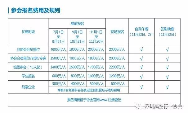
Event Preview
More invited units and report themes are continuously updated!
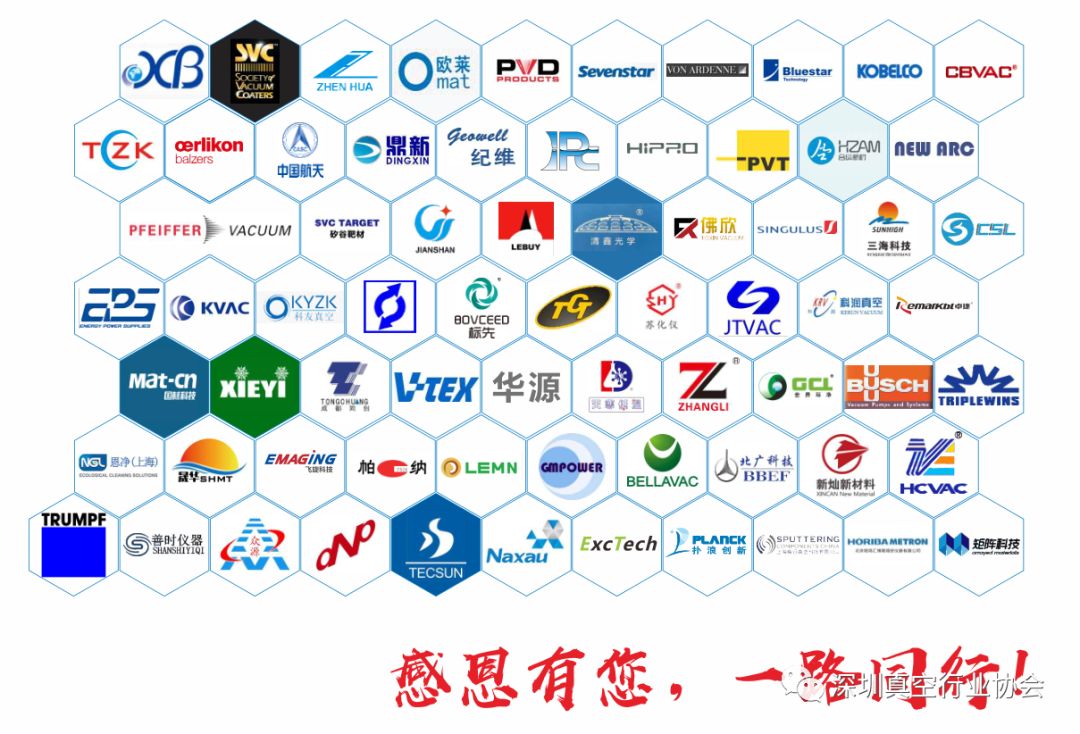
VCCS Past Exhibitors/Sponsors (Partial)
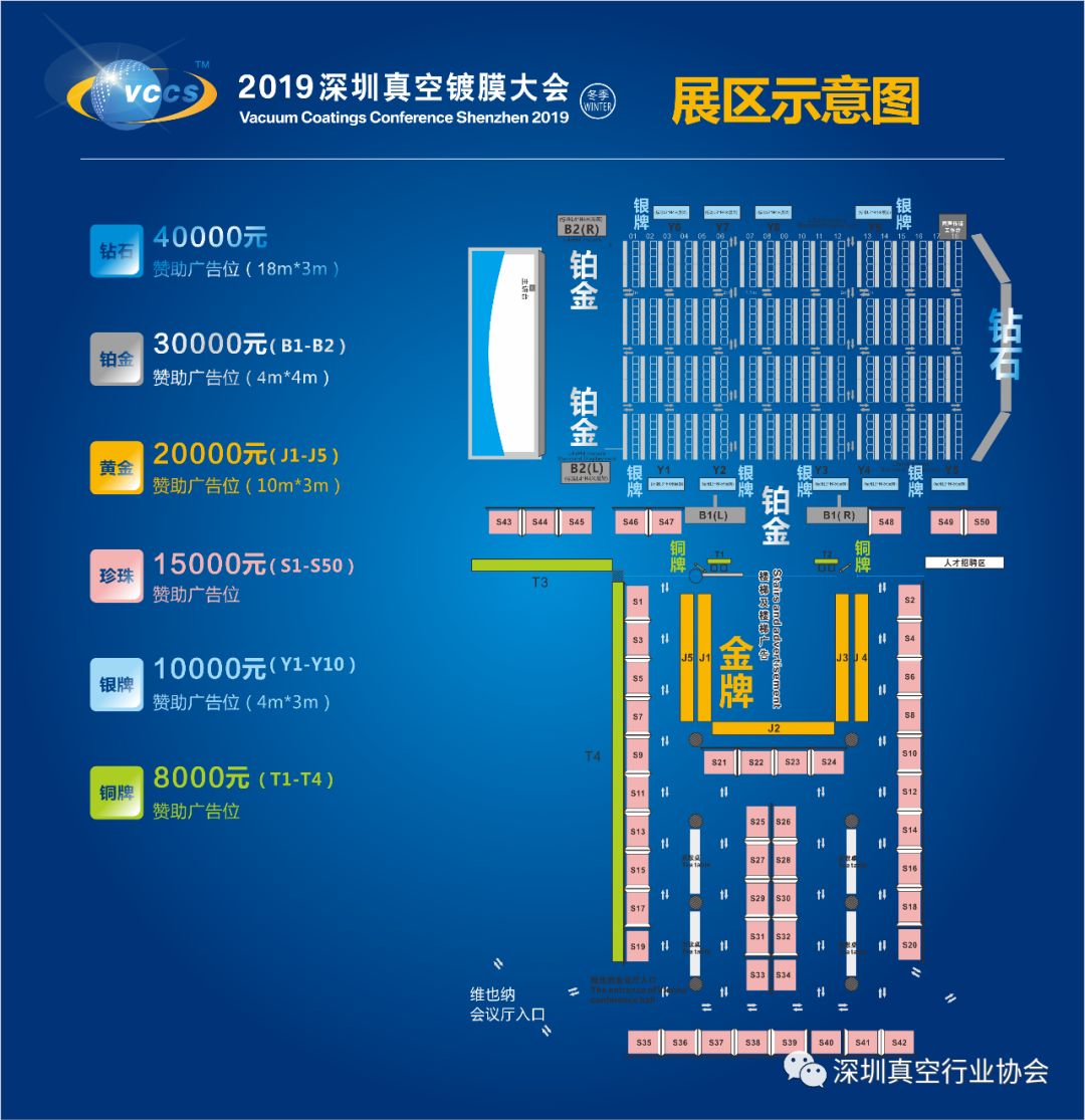
Welcome to Sponsor
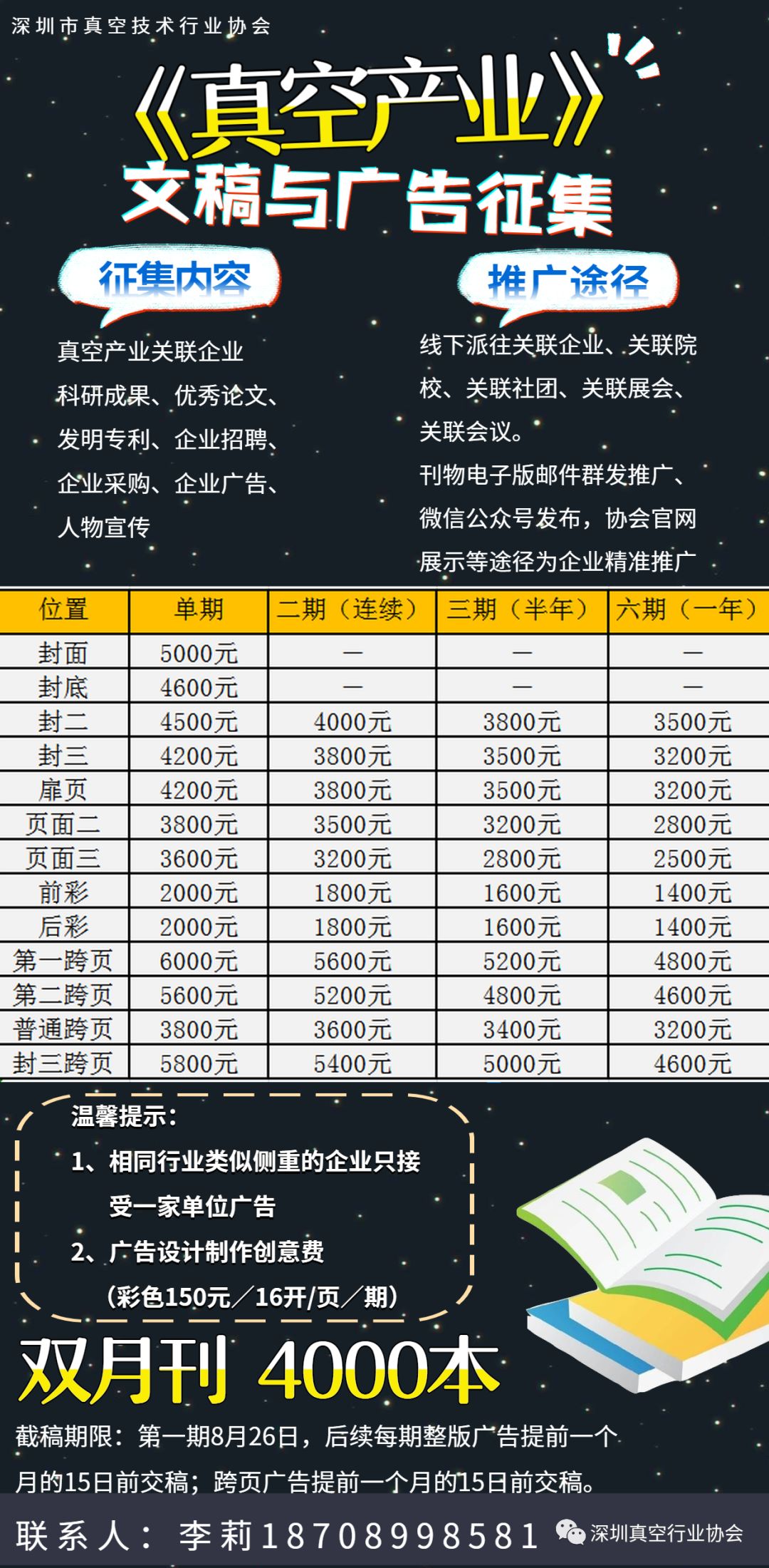
For booth/advertisement reservations and details, please contact:
Ms. Huang 13670231076
Ms. Li 18708998581
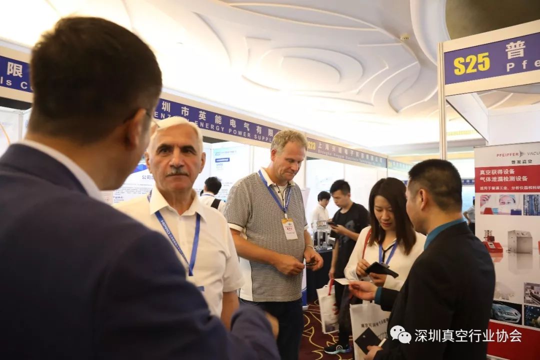
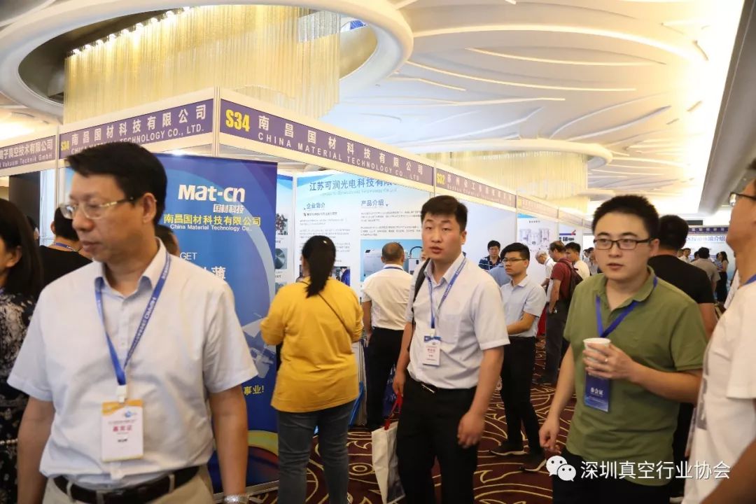
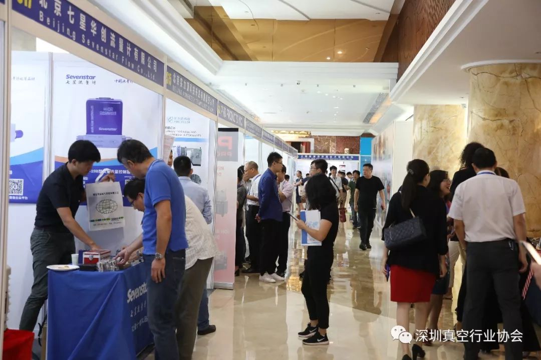
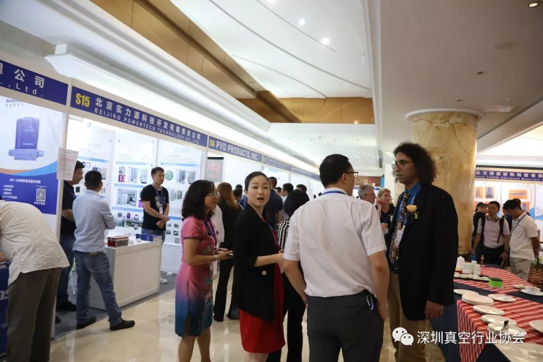
On-site Booth Images

Articles You May Like
► VCCS2019 Shenzhen Vacuum Coating Conference (Summer) Successfully Held!
► You are cordially invited to join the Vacuum Technology and Applications Club
► Conference Preview | VCCS2019 Shenzhen Vacuum Coating Conference (Winter)
► Why Participate in Exhibitions and Conferences? We Provide You with a Definitive Answer!
Click Read Original Text to Register for the Event Immediately