
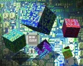
A chip is a way to miniaturize circuits in electronics, mainly including semiconductor devices and passive components, and is usually manufactured on the surface of semiconductor wafers.
The aforementioned integrated circuits manufactured on the surface of semiconductor chips are also known as thin-film integrated circuits; another type of thick-film hybrid integrated circuit is composed of independent semiconductor devices and passive components integrated into a substrate or circuit board to form a miniaturized circuit.
The integrated circuit industry is characterized by a winner-takes-all approach. Giants like Intel can achieve profits of up to 60% at their peak. So, what is the actual cost of a CPU that can easily cost hundreds or thousands of yuan?
First, let’s take a look at the manufacturing process
The complete process of chip manufacturing includes several stages: chip design, wafer production, packaging production, and cost testing, among which the wafer manufacturing process is particularly complex. The manufacturing process of precision chips is very complicated, starting with chip design, which generates the “pattern” based on design requirements.
1. Raw Material Wafer for Chips
The composition of the wafer is silicon, which is refined from quartz sand. The wafer is purified silicon (99.999%), then these pure silicon materials are made into silicon ingots, which are the quartz semiconductor materials used for manufacturing integrated circuits. Slicing these ingots produces the wafers needed for chip manufacturing. The thinner the wafer, the lower the production cost, but the requirements for the process become higher.
2. Wafer Coating
The wafer coating can resist oxidation and has temperature resistance, and its material is a type of photoresist.
3. Wafer Photolithography, Development, and Etching
This process uses a chemical substance sensitive to ultraviolet light, which softens when exposed to UV light. By controlling the position of the mask, the shape of the chip can be obtained. A photoresist is applied to the silicon wafer, which will dissolve when exposed to UV light. At this point, the first mask can be used to dissolve the parts exposed to UV light, which can then be washed away with a solvent. The remaining parts will match the shape of the mask, which is the desired effect. This way, we obtain the silicon dioxide layer we need.
4. Doping Impurities
Ions are implanted into the wafer to generate corresponding P and N type semiconductors. The specific process starts from the exposed area on the silicon wafer, where a chemical ion mixture is introduced.
This process changes the conductivity of the doped area, allowing each transistor to be turned on, off, or carry data. Simple chips may only require one layer, but complex chips usually have many layers, in which case this process is repeated continuously, with different layers connected through opened windows. This is similar to the manufacturing principle of multi-layer PCB boards. More complex chips may require multiple silicon dioxide layers, achieved by repeating photolithography and the above processes to form a three-dimensional structure.
5. Wafer Testing
After the aforementioned processes, a grid of grains forms on the wafer. Each grain undergoes electrical characteristic testing using needle testing. Generally, the number of grains per chip is enormous, and organizing a needle testing mode is a very complex process, requiring the production of batches of chips with the same specifications. The larger the quantity, the lower the relative cost, which is also why mainstream chip devices are cheaper.
6. Packaging
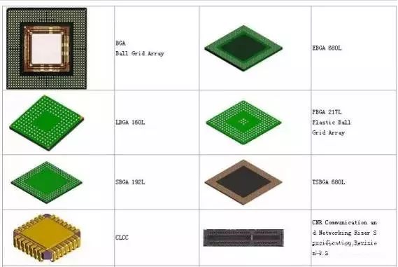
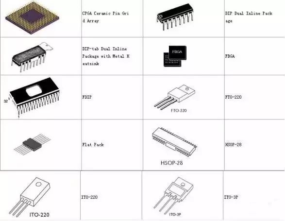
The completed wafer is fixed, pins are bonded, and various packaging forms are produced according to requirements. This is why the same chip core can have different packaging forms, such as DIP, QFP, PLCC, QFN, etc. This is mainly determined by external factors such as user application habits, application environment, and market conditions.
7. Testing and Packaging
After the above process, chip manufacturing is completed. This step involves testing the chips, eliminating defective products, and packaging.
Composition of Chip Hardware Costs
The cost of a chip includes both the hardware cost and the design cost of the chip.
The hardware cost of the chip includes four parts: wafer cost + mask cost + testing cost + packaging cost (for IC design companies in the ARM camp, they need to pay ARM design research and development fees and royalties for each chip, but here we mainly describe independent CPUs and giants like Intel, avoiding the cost of purchasing IP), and we also need to exclude those waste chips from testing and packaging.
Expressed as a formula:
Chip Hardware Cost = (Wafer Cost + Testing Cost + Packaging Cost + Mask Cost) / Final Yield
(A brief explanation of the above terms for better understanding by the general public; those in the know can skip this.)
From silicon dioxide to the chips sold on the market, it goes through the processes of producing industrial silicon, producing electronic silicon, and then cutting and polishing to produce wafers. The wafer is the raw material for chip manufacturing, and the wafer cost can be understood as the cost of the materials (silicon wafers) used for each chip.
Generally, especially when the production volume is large enough and has independent intellectual property rights, when calculated in units of hundreds of millions, the wafer cost occupies the highest proportion. However, there are exceptions, which will be introduced in the packaging cost section.
Packaging involves stacking the substrate, core, and heat sink together to form the CPUs we commonly see. The packaging cost is the funds required for this process. In general cases of large production volumes, the packaging cost usually accounts for about 5% to 25% of the hardware cost, but some IBM chips have packaging costs accounting for about half of the total cost, with reports of it reaching as high as 70% at one time.
Testing can identify key characteristics of each processor, such as maximum frequency, power consumption, heat generation, etc., and determine the grade of the processor, classifying a batch of chips into categories such as I5 4460, I5 4590, I5 4690, I5 4690K, etc. Intel can then set different prices based on different grades. However, if the chip production volume is large enough, the testing cost can be negligible.
Mask cost refers to the cost required for different process technologies. For example, the cost of masks for the 40/28nm process is already very mature and low—$2 million for the 40nm low-power process; $4 million for the 28nm SOI process; and $6 million for the 28nm HKMG process.
However, at the beginning of advanced process technologies, the costs were quite high—in 2014, when the 14nm process was first introduced, its mask cost was $300 million (as time passes and TSMC and Samsung master the 14/16nm processes, the current price should not be this high); and Intel is currently developing the 10nm process. According to Intel’s official estimates, the mask cost will require at least $1 billion.
However, if chips are produced in units of hundreds of millions (it seems like Apple’s annual shipments of phones and tablets are in the hundreds of millions), even if the mask cost reaches $1 billion, the cost allocated to each chip would only be $10. This reflects why giants like Apple use TSMC and Samsung’s most advanced and most expensive process technologies and still make huge profits, which is why IC design has a winner-takes-all characteristic.
Costs incurred for steps such as photolithography, etching, ion implantation, metal deposition, metal layers, interconnections, wafer testing and cutting, core packaging, and grade testing, as well as the depreciation costs of manufacturing equipment such as photolithography machines, etching machines, thinning machines, dicing machines, bonding machines, and flip chip machines, are included in the testing cost, packaging cost, and mask cost, so there is no need to calculate them separately.
Cost of Chips
Since it is impossible to guarantee 100% utilization when processing and cutting wafers into chips, there is a yield issue. Therefore, the cost of chips is expressed as:
Chip Cost = Wafer Cost / (Number of Chips per Wafer * Chip Yield)
Since wafers are round and chips are rectangular, some edge materials will inevitably be wasted, so the number of chips that can be cut from each wafer cannot simply be calculated by dividing the area of the wafer by the area of the chip; instead, the following formula must be used:
Number of Chips per Wafer = (Area of Wafer / Area of Chip) – (Perimeter of Wafer / (2 * Area of Chip) ^ 0.5)
The chip yield is closely related to process complexity and the number of defects per unit area, and the yield can be expressed as:
Chip Yield = (1 + B * Chip Cost / A) ^ (-A)
A is the process complexity; for example, the complexity of a self-developed CPU-X using 40nm low-power technology is between 2 and 3;
B is the number of defects per unit area; for a self-developed CPU-X using 40nm technology, the number of defects per unit area is between 0.4 and 0.6.
Assuming that the self-developed CPU-X is approximately 15.8mm long and 12.8mm wide (the aspect ratio of 37:30, controlling a quad-core chip’s aspect ratio within this proportion is not easy), the area is approximately 200 square millimeters (for ease of calculation, the decimal is omitted).
A 12-inch wafer has an area of approximately 70,000 square millimeters, so a wafer can accommodate 299 self-developed CPU-X chips. By substituting a=3 and b=0.5 into the chip yield formula, the yield is 49%, meaning that a 12-inch wafer can produce 146 good chips, and the price of a 12-inch wafer is $4,000, leading to a cost of $28 per chip.
Calculation of Chip Hardware Costs
The costs of packaging and testing do not have specific formulas; however, the testing price is roughly proportional to the square of the number of pins, while the packaging cost is roughly proportional to the product of the number of pins and the cube of the power consumption. If the CPU-X uses a self-developed chip with 40nm low-power technology, the testing cost is approximately $2, and the packaging cost is approximately $6.
Since the mask cost for the 40nm low-power process is $2 million, if the self-developed CPU-X sells 100,000 units, the mask cost will be $20. By substituting the testing cost = $2, packaging cost = $6, and chip cost = $28 into the formula, the chip hardware cost = (20 + 2 + 6) / 0.49 + 28 = $85.
The hardware cost of the self-developed CPU-X is $85.
If the self-developed CPU-Y uses 28nm SOI technology and the estimated chip area is 140 square millimeters, then 495 CPUs can be cut from it. Since 28nm and 40nm processes are both very mature technologies, the cutting cost’s impact is minimal. Thus, the wafer price can still be calculated at $4,000, and the chip yield is also calculated at 49%. A 12-inch wafer can cut 242 chips, and the cost per chip is $16.
If the self-developed CPU-Y sells 100,000 units, the mask cost will be $40. According to the packaging and testing costs accounting for approximately 20% of the total chip cost and a chip yield of 49%, the hardware cost of the chip is $122.
If the self-developed chip’s production volume is 1 million, the mask cost will be $4, and according to the packaging and testing costs accounting for approximately 20% of the total chip cost, the hardware cost of the chip is $30.
If the self-developed chip’s production volume is 10 million, the mask cost will be $0.4, and according to the packaging and testing costs accounting for approximately 20% of the total chip cost, the hardware cost of the chip is $21.
It is evident that under the same production volume, using more advanced process technologies will increase the hardware cost of chips, but as long as the production volume is large enough, the originally high costs can be spread over large quantities, significantly reducing the cost of chips.
Pricing of Chips
The hardware cost is relatively clear, but the design cost is more complex. This includes the salaries of engineers, costs for EDA and other development tools, equipment costs, site costs, etc.
Additionally, a significant portion is the IP cost—if it is a self-developed CPU, it is manageable (certain self-developed microstructures can be done without third-party IP). However, for ARM camp IC design companies, a large amount of external IP needs to be purchased, and these IPs are expensive, making it difficult to quantify the design costs of domestic and foreign IC design companies uniformly.
According to the universally accepted pricing strategy for low-profit chip design companies, the 8:20 pricing method states that when the hardware cost is 8, the price is set at 20. Under a production volume of 100,000 units, the self-developed CPU-X is priced at $212.
Don’t think this pricing is high; it is actually quite low. Intel generally uses a pricing strategy of 8:35, and AMD has historically reached 8:50.
Under a production volume of 100,000 units, the self-developed CPU-Y also uses the 8:20 pricing method, with a price of $305;
Under a production volume of 1 million, the self-developed CPU-Y also uses the 8:20 pricing method, with a price of $75;
Under a production volume of 10 million, the self-developed CPU-Y also uses the 8:20 pricing method, with a price of $52.5.
From this, it can be seen that to reduce the cost/price of CPUs, production volume is crucial, which is also the key reason why Intel and Apple can use relatively expensive process technologies while still making excess profits.
Note:This article is reprinted from 满天芯. Thanks to the original author for their contribution. If your related rights are infringed, please contact the backend, and we will handle it promptly!
Edited by: Xiao Zhang