For more exciting content, please click the blue words above to follow us
Source: Zuo Si Automotive Research, Zhou Yanwu
ARM has launched a series of CPU architectures for autonomous driving, all of which comply with automotive functional safety, namely A65AE, A76AE, and A78AE, where AE stands for automotive-grade enhanced.
ARM Autonomous Driving Computing Platform Configuration
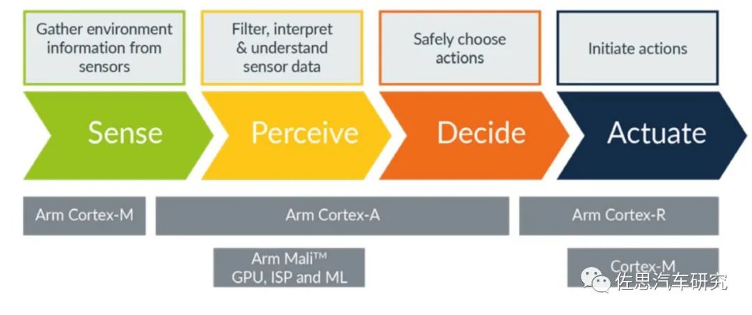
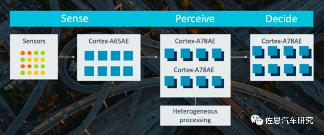
Image Source: Internet
ARM’s Split/Lock/Hybrid Modes for Automotive Functional Safety
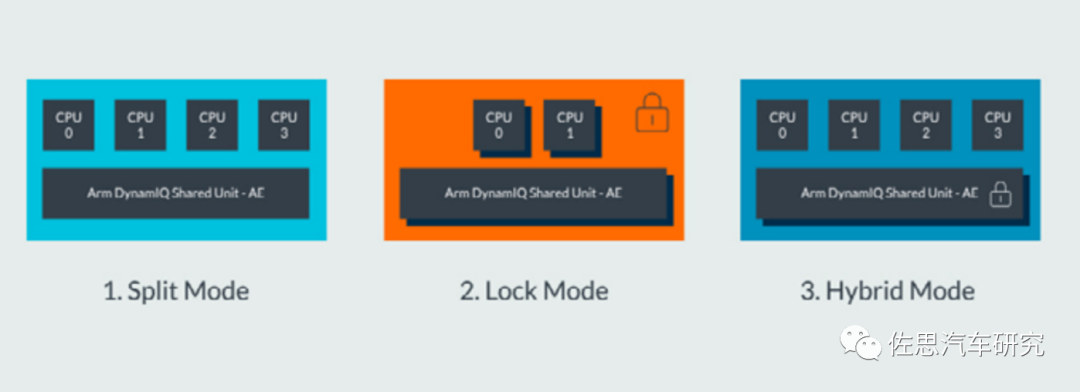
Image Source: Internet
In the automotive functional safety standard ISO26262-5 2018 product development: hardware level appendix D, the recommended safety technical measures for the diagnostic coverage of processing units include several technical measures that can achieve high diagnostic coverage, among which hardware redundancy technology, dual-core lockstep, asymmetric redundancy, and coding calculation are three typical technical measures.
Lockstep means that two cores run the same program, inputting the results into a comparison logic, periodically comparing whether the outputs of the two cores are the same, i.e., CCM. If they are the same, they continue running; otherwise, certain measures need to be taken. If the error still exists after a period of time, a restart or recheck may be necessary. The design of lockstep cores is fixed in the chip design, so there is no adjustability. It is easy to see that although lockstep cores use two cores, they actually only serve the function of one core, wasting one core. This method has been successfully validated in microcontrollers and lower complexity microprocessor fields for many years. If the core design is more complex, even if there are no anomalies, the two cores may not synchronize. Currently, further developments involve outputting the comparison results to a core known as the “safety island,” which is responsible for decision-making and execution. This core uses a separate clock and power supply, and has very high safety performance. ARM generally recommends the Cortex-R52.
ARM has dual lockstep capabilities, the first within the CPU, implemented through the DSU, and the second externally through the safety island. The DSU is the DynamIQ Shared Unit, which first appeared in the A75.
ARM DSU Application Example
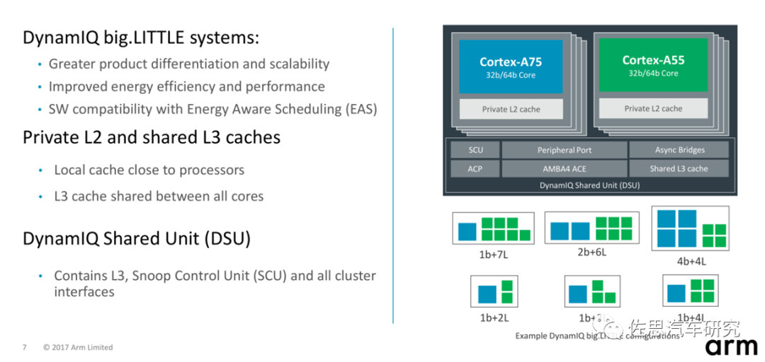
Image Source: Internet
Basic Structure of DSU
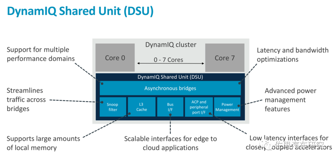
Image Source: Internet
The core function of the DSU is to control the CPU cores to use them in clusters. Each core in the cluster can be individually turned on and off, and frequency/voltage can be adjusted, resulting in better energy efficiency. Manufacturers can even place different cores (currently only supporting Cortex-A75 and Cortex-A55) in a cluster in an unequal number, such as Cortex-A75×3 + Cortex-A55×5, or Cortex-A75×1 + Cortex-A55×7, balancing cost and performance. Additionally, there is shared L3 cache. The DSU can use different bus technologies such as CCI, CCN, or CMN to connect the CPU with other units in the SoC (GPU, Modem, memory) at high speed; if it has 4MB of L3 cache, it can dynamically allocate the cache to each core, for example, in the case of Cortex-A75×1 + Cortex-A55×7, 3MB of cache can be allocated to the A75 core, while the remaining 7 A55 cores share 1MB of cache, and it can even allocate the L3 cache for use by GPU and other units, providing very high flexibility; most importantly, it also controls the power states, frequency, and voltage of each CPU core in the cluster, which is key to controlling CPU performance and power consumption.
When designing DynamIQ, ARM also considered redundancy requirements. For example, compared to smartphones, automotive reliability and redundancy requirements are much higher. DynamIQ allows multiple clusters to connect via CCIX, so processors can be distributed in different locations in the vehicle. When a traffic accident occurs and one cluster is damaged, the DynamIQ technology can call upon a backup processor to ensure the normal operation of the vehicle.
Cortex-A78AE’s DSU AE Internal Framework Diagram
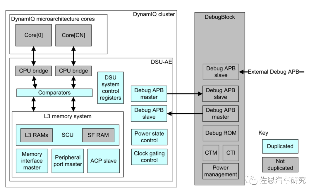
Image Source: Internet
DSU AE mainly adds comparators, and the highlighted parts are duplicated, including execution logic, clock, power states, various interfaces; of course, the cache cannot be duplicated, as that would be too costly and not very meaningful.
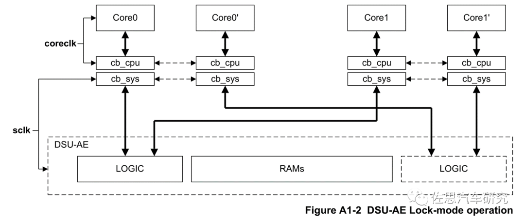
Image Source: Internet
DSU-AE Separation Mode
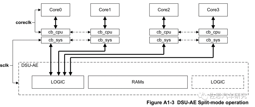
Image Source: Internet
DSU-AE Hybrid Mode
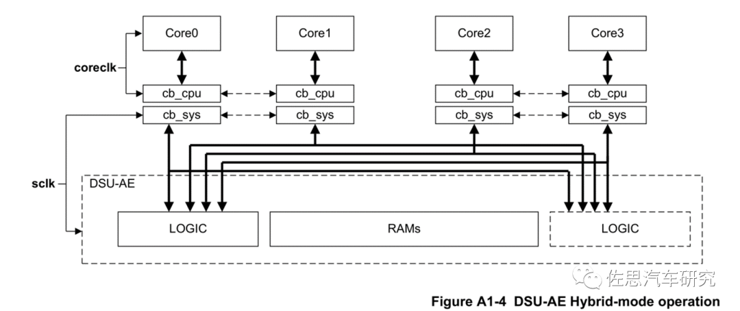
Image Source: Internet
DSU-AE Interface
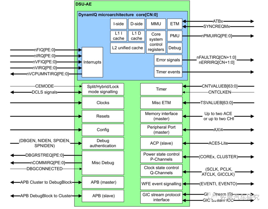
Image Source: Internet
In addition to the DSU, there are GPU architectures G78AE, image ISP C71AE, interrupt controller GIC-600AE, memory management MMU-600AE, and mesh bus CMN-600AE for automotive functional safety. However, the DSU is the most critical.
Second, ARM‘s On-Chip Bus
Complete Series of ARM Smart Driving Products
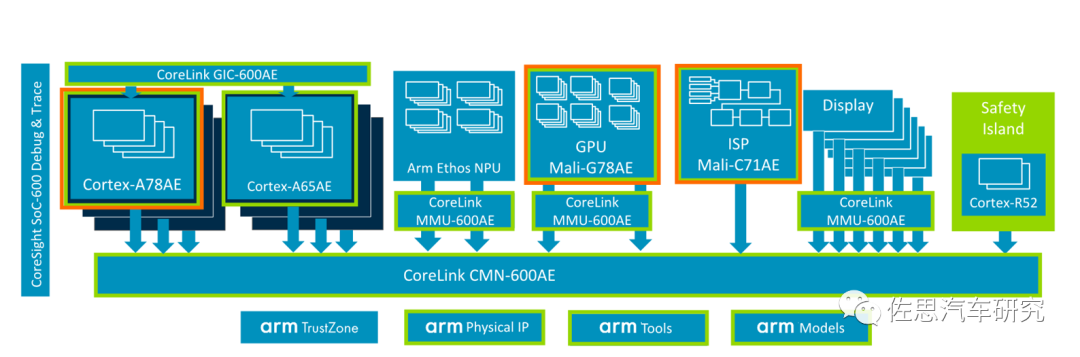
Image Source: Internet
Digital IC has evolved from a timing-driven design method to an IP-reuse-based design method, which has been widely applied in SoC design. In IP-reuse-based SoC design, the on-chip bus is the core system that connects various modules and arbitrates among them, making it the most critical issue in design. The AMBA bus is a special mechanism developed by ARM (Advanced Microcontroller Bus Architecture) that integrates RISC processors with other IP cores and peripherals, effectively connecting IP cores as a “digital glue” and is an important component of ARM’s reuse strategy. It is not an interface between the chip and peripherals, but an interface for communication between ARM cores and other components on the chip. The AMBA specification mainly includes the AHB (Advanced High-Performance Bus) system bus and the APB (Advanced Peripheral Bus) peripheral bus. In addition to the AMBA bus, ARM also has GIC interrupt control for multi-core systems and MMC memory control.
ARM CMN-700
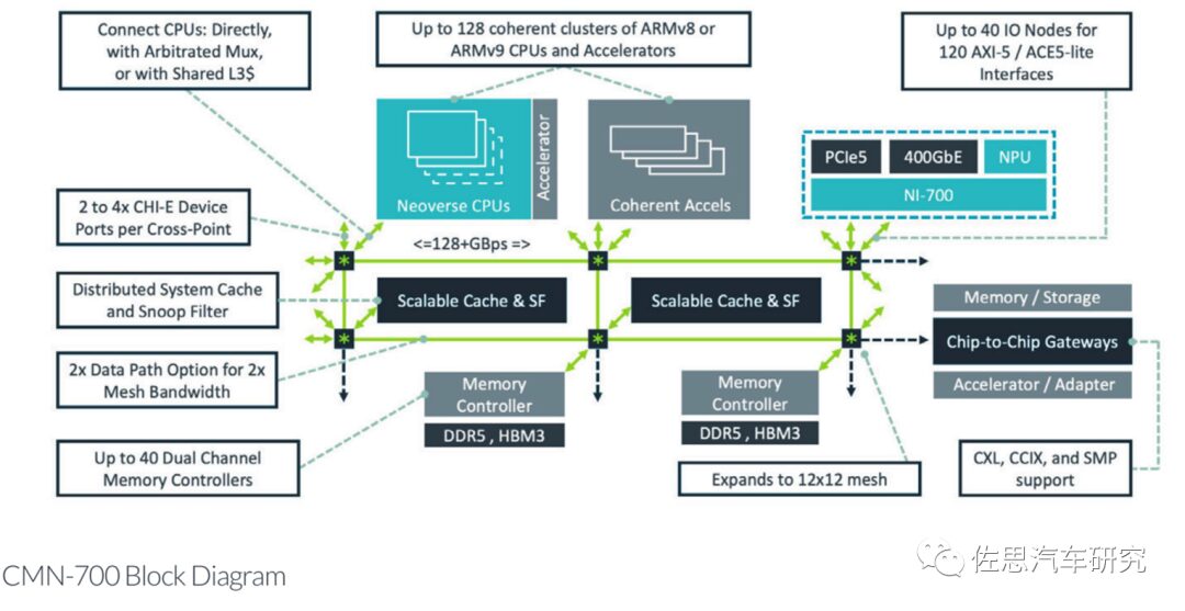
Image Source: Internet
ARM has developed a connection system that lies between a bus and NoC, called CMN, primarily used for connecting CPU cores, but also for connections between CPU cores and accelerators. It adopts a MESH grid structure but lacks routing functionality; it is essentially still a bus, but the MESH grid supports many more units than a typical bus, supporting up to 512 cores and 512MB of L3 cache, with the main target market being the HPC field.
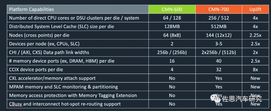
CMN-700 also supports AMBA AXI5, ACE5-lite, CXS and CCIX
Appendix: Overview of ARM Architecture
Scan to learn more industry news