Click the image to view details
ARM has launched a series of CPU architectures for autonomous driving, all of which comply with automotive functional safety: A65AE, A76AE, and A78AE, where AE stands for automotive-grade enhanced.
ARM Autonomous Driving Computing Platform Configuration


Image source: Internet
ARM’s Split/Lock/Hybrid Modes for Automotive Functional Safety

Image source: Internet
In the automotive functional safety standard ISO26262-5 2018 product development: hardware layer appendix D, several safety technical measures are recommended for the diagnostic coverage of processing units, among which hardware redundancy technology, dual-core lock-step, asymmetric redundancy, and coded computing are three typical technical measures.
Lock-step is when two cores run the same program and input the results into a comparison logic, periodically comparing whether the outputs of the two cores are the same, i.e., CCM. If they are the same, they continue to run; otherwise, certain measures need to be taken. If an error persists after a period, a restart or re-check may be necessary. The design of lock-step cores is fixed in chip design, so there is no adjustability. It is easy to see that although lock-step cores use two cores, they effectively only function as one, wasting one core. This method has been successfully validated over many years in microcontrollers and lower complexity microprocessors. If the core design is more complex, even without abnormalities, the two cores may not synchronize. Currently, the next step is to output the comparison results to a core referred to as a “safety island,” responsible for decision-making and execution. This core uses a separate clock and power source and has high safety performance. This solution increases system complexity but allows for more flexible software execution. ARM generally recommends the Cortex-R52.
ARM has dual lock-step capability, the first within the CPU, realized by the DSU, and the second externally, utilizing the safety island. The DSU is the DynamIQ Shared Unit, first appearing in the A75.
ARM DSU Application Example

Image source: Internet
Basic Composition of DSU

Image source: Internet
The core function of the DSU is to control the CPU cores to form clusters. Each core within the cluster can be turned on/off individually, and frequency/voltage can be adjusted for better energy efficiency. Manufacturers can even place different cores (currently only Cortex-A75 and Cortex-A55) in a cluster in an unequal number, such as Cortex-A75×3+ Cortex-A55×5 or Cortex-A75×1+ Cortex-A55×7, balancing cost and performance. Additionally, there is shared L3 cache. The DSU can use different bus technologies such as CCI, CCN, or CMN to connect the CPU with other units in the SoC (GPU, Modem, memory) at high speed; if it has 4MB of L3 cache, it can dynamically allocate cache to each core. For example, with Cortex-A75×1+ Cortex-A55×7, it can allocate 3MB of cache to the A75 core, with the remaining 7 A55 cores sharing 1MB of cache, and it can even allocate the L3 cache to the GPU and other units, providing high flexibility; most importantly, it also controls the switching, frequency, and voltage of each CPU core within the cluster, which is key to controlling CPU performance and power consumption.
When designing DynamIQ, ARM also considered redundancy needs, such as the higher reliability and redundancy requirements in vehicles compared to smartphones. DynamIQ allows multiple clusters to be connected through CCIX, enabling processors to be distributed across different locations in the vehicle. In the event of an accident, if one cluster is damaged, DynamIQ technology can call upon backup processors to ensure normal vehicle operation.
DSUAE Internal Framework Diagram of Cortex-A78AE
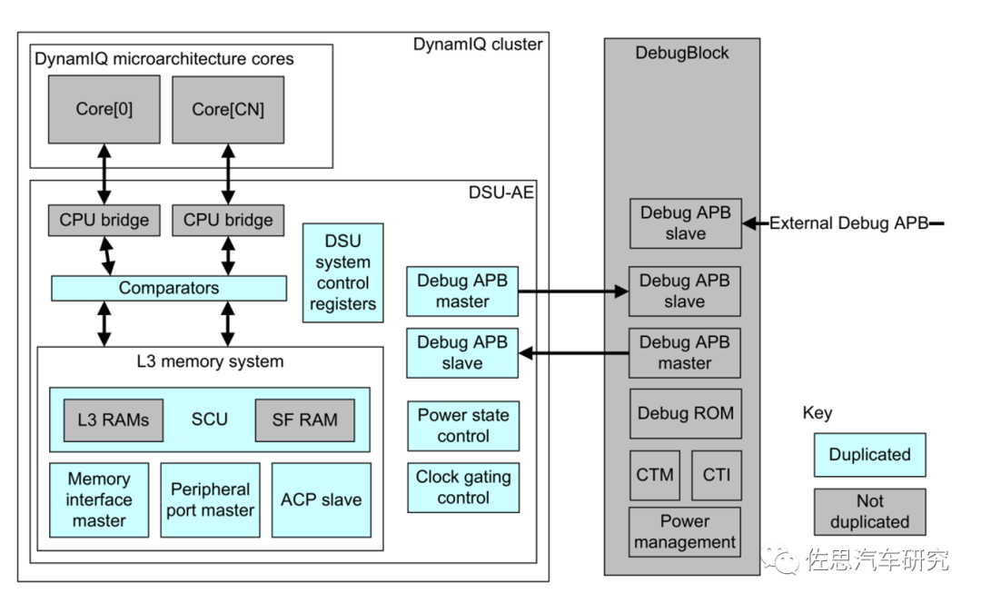
Image source: Internet
DSU AE mainly adds comparators, and the bright-colored parts are duplicated, including execution logic, clocks, power states, and various interfaces. However, the cache cannot be duplicated as that would be too costly and not very meaningful.

Image source: Internet
DSU-AE Separation Mode

Image source: Internet
DSU-AE Hybrid Mode

Image source: Internet
DSU-AE Interface

Image source: Internet
In addition to DSU, there are also GPU architectures G78AE for automotive functional safety, image ISP C71AE, interrupt controller GIC-600AE, memory management MMU-600AE, and mesh bus CMN-600AE. But the DSU is the most critical.
II. ARM’s on-chip bus
ARM Smart Driving Product Series

Image source: Internet
Digital IC has evolved from a timing-driven design approach to an IP reuse-based design approach, which has been widely applied in SoC design. In IP reuse-based SoC design, the on-chip bus is the core system that connects various modules and arbitrates between them, making it the most critical issue in design. The AMBA bus is a special mechanism developed by ARM (Advanced Microcontroller Bus Architecture) that integrates RISC processors with other IP cores and peripherals, effectively connecting IP cores as the “digital glue” and is an important component of ARM’s reuse strategy. It is not an interface between the chip and peripherals, but an interface for communication between ARM cores and other components on the chip. The AMBA specification mainly includes the AHB (Advanced High-Performance Bus) system bus and APB (Advanced Peripheral Bus) peripheral bus. In addition to the AMBA bus, ARM also has GIC interrupt control for multi-core and MMC memory control.
ARM CMN-700

Image source: Internet
ARM has developed a connection system between a bus and NoC, called CMN, primarily used to connect CPU cores, and can also connect CPU cores with accelerators. It adopts a MESH grid structure but lacks routing functionality; it is essentially still a bus, but the MESH grid supports many units, far exceeding a general bus, supporting up to 512 cores and 512MB of L3 cache, targeting the HPC market.

CMN-700 also supports AMBA AXI5, ACE5-lite, CXS, and CCIX
Appendix: Overview of ARM Architecture


Understanding Automotive System-on-Chip SoC: Part 6: CPU Microarchitecture
Understanding Automotive System-on-Chip SoC: Part 5: Instruction Set and Computing Architecture
Understanding Automotive System-on-Chip SoC: Part 4: Cache, Superscalar, Out-of-Order Execution
Understanding Automotive System-on-Chip SoC: Part 3: ARM’s Business Model and Overview of CPU Microarchitecture
Understanding Automotive System-on-Chip SoC: Part 2: Automotive Chip Industry and Supply Chain
Understanding Automotive System-on-Chip SoC: Part 1: Overview of Automotive System-on-Chip and AEC-Q100 Automotive Standards
Report Ordering and Cooperation Consulting Contact:
Zuo Yan Jun: 18600021096 (same WeChat)
Zosi 2022 Research Report Writing Plan
Smart Connected Vehicle Industry Chain Overview (February 2022 Edition)
| Mainframe Factory Autonomous Driving |
Automotive Vision (Upper) |
High-Precision Map |
| Commercial Vehicle Autonomous Driving |
Automotive Vision (Lower) |
High-Precision Positioning |
| Low-Speed Autonomous Driving |
Automotive Simulation (Upper) |
OEM Information Security |
| ADAS and Autonomous Driving Tier 1 |
Automotive Simulation (Lower) |
Automotive Gateway |
| Automotive and Domain Controller |
Millimeter Wave Radar |
APA and AVP |
| Domain Controller Ranking Analysis |
Vehicle Laser Radar |
Driver Monitoring |
| Laser and Millimeter Wave Radar Ranking |
Vehicle Ultrasonic Radar |
Infrared Night Vision |
| E/E Architecture |
Radar Disassembly |
In-Vehicle Voice |
| Automotive Car-Sharing |
Charging Infrastructure |
Human-Machine Interaction |
| Shared Mobility and Autonomous Driving |
Automotive Motor Controller |
L4 Autonomous Driving |
| EV Thermal Management System |
Hybrid Power Report |
L2 Autonomous Driving |
| Automotive Power Electronics |
Automotive PCB Research |
Fuel Cell |
| Wireless Communication Module |
Automotive IGBT |
Automotive OS Research |
| Automotive 5G |
Automotive Wiring Harness |
Steer-by-Wire Chassis |
| Joint Venture Brand Vehicle Networking |
V2X and Vehicle Road Coordination |
Steering System |
| Independent Brand Vehicle Networking |
Roadside Intelligent Perception |
Modular Report |
| Independent Brand ADAS Research |
Commercial Vehicle Networking |
Commercial Vehicle ADAS |
| Automotive Multi-Modal Interaction |
Automotive Intelligent Cockpit |
In-Vehicle Display |
| Tier 1 Intelligent Cockpit (Upper) |
Cockpit Multi-Screen and Linked Screen |
Smart Rearview Mirror |
| Tier 1 Intelligent Cockpit (Lower) |
Intelligent Cockpit Design |
Automotive Lighting |
| Cockpit SOC |
Automotive VCU Research |
Automotive Seats |
| Automotive Digital Key |
TSP Manufacturers and Products |
HUD Industry Research |
| Automotive Cloud Service Research |
OTA Research
|
Automotive MCU Research |
| AUTOSAR Research |
Smart Parking Research |
Sensor Chips |
| Software Defined Vehicles |
Waymo Smart Connected Layout |
ADAS/AD Main Control Chip |
| T-Box Market Research |
Autonomous Driving Regulations |
ADAS Data Annual Report |
| T-Box Ranking Analysis |
Smart Connected and Autonomous Driving Base |
Automotive Magnesium Alloy Die Casting |
| Passenger Car Camera Quarterly Report |
Smart Vehicle Personalization |
Flying Cars |
| Special Vehicle Autonomous Driving |
Agricultural Machinery Autonomous Driving |
Mining Autonomous Driving |
| Port Autonomous Driving |
Autonomous Heavy Trucks |
Unmanned Shuttle
|
| Instrument and Central Control Display |
In-Vehicle DMS |
Joint Venture Brand ADAS |
| Surround View Market Research (Domestic Edition) |
800V High-Voltage Platform |
Commercial Vehicle ADAS |
| Surround View Market Research (Joint Venture Edition) |
Automotive Wireless Module |
EDR Industry Research |
「Zosi Research Monthly Report」
ADAS/Smart Vehicle Monthly Report | Automotive Cockpit Electronics Monthly Report | Automotive Vision and Radar Monthly Report | Battery, Motor, Electric Control Monthly Report | In-Vehicle Information System Monthly Report | Passenger Car ACC Data Monthly Report | Front View Data Monthly Report | HUD Monthly Report | AEB Monthly Report | APA Data Monthly Report | LKS Data Monthly Report | Front Radar Data Monthly Report