 Any practical electronic application will be affected by multiple sources of error, which can cause even the most precise components to deviate from their specified behavior in the datasheet. When the application signal chain lacks built-in mechanisms to self-correct these errors, the only way to minimize their impact is to measure the errors and systematically calibrate them.
Open-loop systems do not use the output to adjust the control operation at the input to achieve the desired performance, while in closed-loop systems, the output depends on the system’s control operation, allowing the system to automatically implement corrections to improve performance. Most digital-to-analog converter (DAC) signal chains are of the “set-and-forget” type, where the accuracy of the output depends on the precision of each module in the signal chain. The “set-and-forget” type system is an open-loop system. For open-loop systems that require high precision, calibration is recommended and is likely necessary.
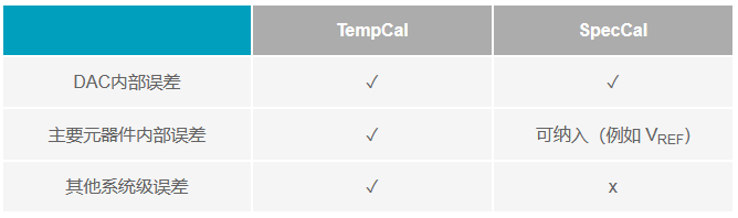
We will introduce two types of DAC signal chain calibration: one is TempCal (temperature calibration), which provides the best level of error correction; the other is SpecCal (specification calibration), which is an effective alternative when TempCal cannot be used, but is not as comprehensive as the former.
 DAC Types
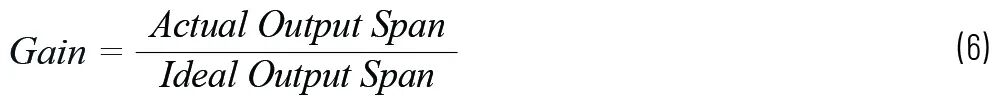
Unipolar voltage DACs can only provide positive or negative output. This article will use the AD5676R as an example of a unipolar DAC to illustrate how to perform precise calibration. The same method can be applied to make necessary adjustments to other types of DACs. Bipolar voltage DACs (such as the AD5766) can provide both positive and negative outputs simultaneously. Current output DACs are often used in multiplication configurations (MDAC) to provide variable gain, and they typically require external amplifiers to buffer the voltage generated across fixed resistors. Precision current source DACs (IDACs), such as the AD5770R and LTC2662, are a new class of DACs that can precisely set output current within a predefined range without any additional external components.
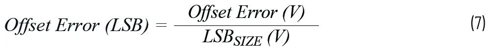
DAC Transfer Function Theory and Internal Errors
The ideal analog output voltage or current generated by a digital-to-analog converter is strictly proportional to the input digital code and is unaffected by external influences such as variations in power supply and reference voltage.
For an ideal voltage output DAC, the incremental increase in output corresponding to a one-step increase in the input digital code is called LSB, defined as follows:
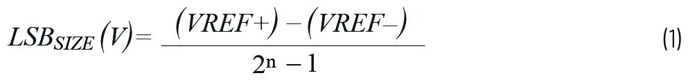
Where:
(VREF+) and (VREF-) are the positive and negative reference voltages, respectively. In some cases, (VREF-) is equal to ground voltage (0 V).
n is the resolution of the DAC, measured in bits.
LSBSIZE (V) is the minimum increment of the DAC output, measured in volts.
This means that for any given input code, once the LSB is known, the DAC’s voltage output should be accurately predictable.

In practice, the accuracy of the DAC output is affected by DAC gain and offset errors (internal errors) as well as other components in the signal chain (system-level errors). For example, some DACs integrate output amplifiers, while others require external amplifiers, which can introduce additional sources of error.
The most relevant technical specifications in the datasheet are defined in the terminology section. For DACs, this section lists parameters such as offset error and gain error.
Zero-level error measures the output error when the zero-level code (0x0000) is loaded into the DAC register.
Figure 1 shows the impact of offset and gain errors on the transfer function of a unipolar voltage DAC.
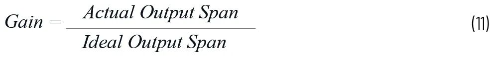
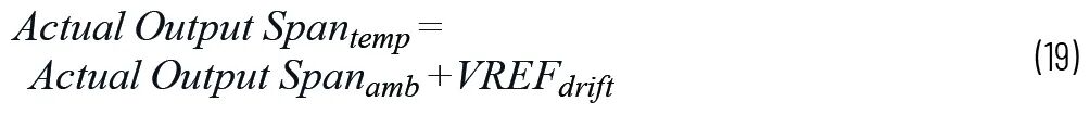
Gain error measures the range error of the DAC, as shown by the purple line in Figure 1. Gain error refers to the deviation of the slope of the DAC transfer characteristic from the ideal value. The ideal DAC transfer characteristic is shown in black.
Offset error refers to the difference between the actual output and the ideal output within the linear region of the transfer function, as shown by the blue line in Figure 1. Note that the blue transfer function uses interpolation to intersect the y-axis, resulting in a negative VOUT, thus determining the offset error.
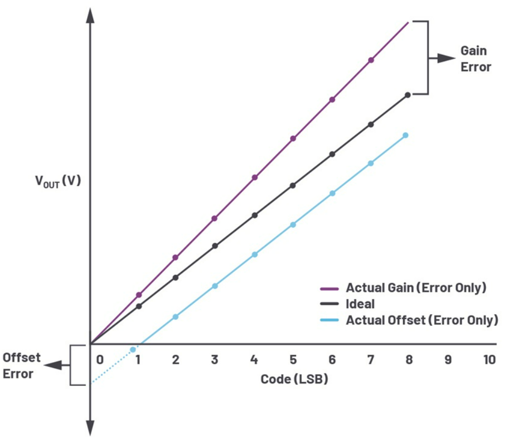
Figure 1. Representation of offset and gain errors for a unipolar DAC.
-
Zero error drift measures the variation of zero error with temperature.
-
Gain error temperature coefficient measures the variation of gain error with temperature.
-
Offset error drift measures the variation of offset error with temperature.
Temperature variations have a significant impact on the accuracy of electronic systems. While the internal gain and offset errors of DACs are typically specified relative to temperature, other components in the system may also affect the total offset and gain of the output.
Therefore, even if the DAC’s INL and DNL are very competitive, other errors, especially temperature-related errors, must be considered. The latest DACs specify total unadjusted error (TUE) to measure the total output error, including all errors—namely INL error, offset error, incremental error, and output drift across power supply voltage and temperature ranges. TUE is expressed as %FSR.
When the datasheet does not specify the DAC’s TUE, a technique called RSS or root-sum-square can be used to calculate TUE, which can sum uncorrelated sources of error for error analysis.

There are also other smaller sources of error, such as output drift, which are often neglected due to their relatively minor impact.
Each specification of every component in the system must be converted to the same unit. This can be accomplished using Table 2.
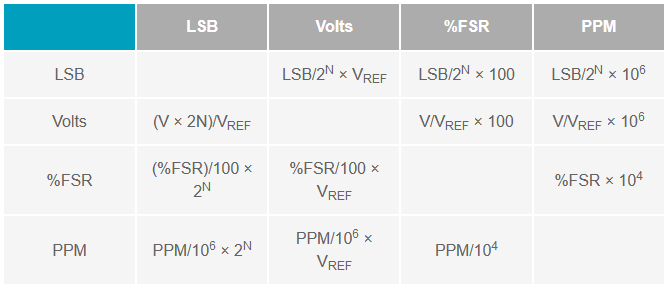
Table 2. Unit Conversion Matrix
TUE is a good metric that succinctly explains how the accuracy of the DC DAC output is affected by all internal errors. However, it does not account for system-level errors, which can vary depending on the signal chain and its environment.
It is worth noting that some DACs have built-in buffer/amplifiers in the output stage, in which case the specifications in the datasheet reflect the impact of both, treating them as part of the internal error.
System-Level Errors
When attempting to analyze the error budget of a given application’s DAC signal chain, system designers should consider and verify the contributions of different components, focusing on the expected operating temperature of the system. Depending on the final application, the signal chain may have many different building blocks, including power ICs, buffers or amplifiers, and various types of active loads, all of which can introduce system-level errors.
Reference Voltage Source
Every DAC relies on a reference voltage source to operate. The reference voltage source is one of the main factors affecting the accuracy of the DAC and the overall signal chain.
The key performance specifications of the reference voltage source are also defined in the separate datasheet for the reference voltage source, such as the ADR45XX series, or as part of the DAC datasheet (if the device has a built-in reference voltage source for user use).
Voltage headroom, sometimes referred to as power supply voltage margin, is defined as the minimum voltage difference between the input voltage required to maintain 0.1% accuracy of the output voltage and the output voltage.
Temperature coefficient (TC or TCVOUT) refers to the relationship between the change in the device’s output voltage and the change in ambient temperature, normalized to the output voltage at 25°C. The TCVOUT of ADR4520/ADR4525/ADR4530/ADR4533/ADR4540/ADR4550 A and B grades has been thoroughly tested at the following three temperatures: −40°C, +25°C, and +125°C. The C grade TCVOUT has been thoroughly tested at the following three temperatures: 0°C, +25°C, and +70°C. This parameter is specified using two methods. The black box method is the most common, considering the temperature coefficient over the entire temperature range; while the tie method can calculate the worst-case slope at +25°C, making it more useful for systems calibrated at +25°C.
For some DACs, the performance of an external reference voltage source may be better than that of an integrated reference voltage source. The reference voltage directly affects the transfer function, so any change in this voltage will proportionally change the slope (i.e., gain) of the transfer function.
It is worth noting that some DACs have built-in buffered reference voltage sources, in which case the specifications in the datasheet reflect the impact of these internal modules, treating them as part of the internal error.
Voltage Regulation Rate
Each independent IC acting as a power supply will define a voltage regulation rate, indicating the change in output in response to a given change in input. This applies to power supplies, buffers, and reference voltage source ICs, which should maintain stable output voltage regardless of input. In the datasheet, the voltage regulation rate is typically specified at ambient temperature.
Load Regulation Rate
Load regulation rate is defined as the incremental change in output voltage with changes in load current. Voltage outputs are typically buffered to mitigate the impact of this change. Some DACs may not buffer the reference input. Therefore, when the digital code changes, the reference input impedance may also change, leading to a change in the reference voltage. Its impact on the output is generally small, but should be considered in high-precision applications. In the datasheet, the load regulation rate is typically specified at ambient temperature.
Solder Thermal Resistance Variation
Solder thermal resistance (SHR) variation is most closely related to the reference voltage source. It refers to the permanent change in output voltage caused by reflow soldering, expressed as a percentage of the output voltage. For more information, refer to the ADR45xx series datasheet. Generally, all ICs are affected by SHR variation to some extent, but this is not always quantifiable, and whether it can be quantified largely depends on the specific system assembly of the application.
Long-Term Stability
Long-term stability defines the change in output voltage over time, expressed in ppm/1000 hours. PCB-level aging treatment can improve the long-term stability of the application.
Open-Loop Calibration Theory
The DAC signal chain schematic is shown in Figure 2. The modules shown in the black box represent a simplified open-loop signal chain, while the modules shown in the gray box are examples of additional components required to implement a closed-loop signal chain.
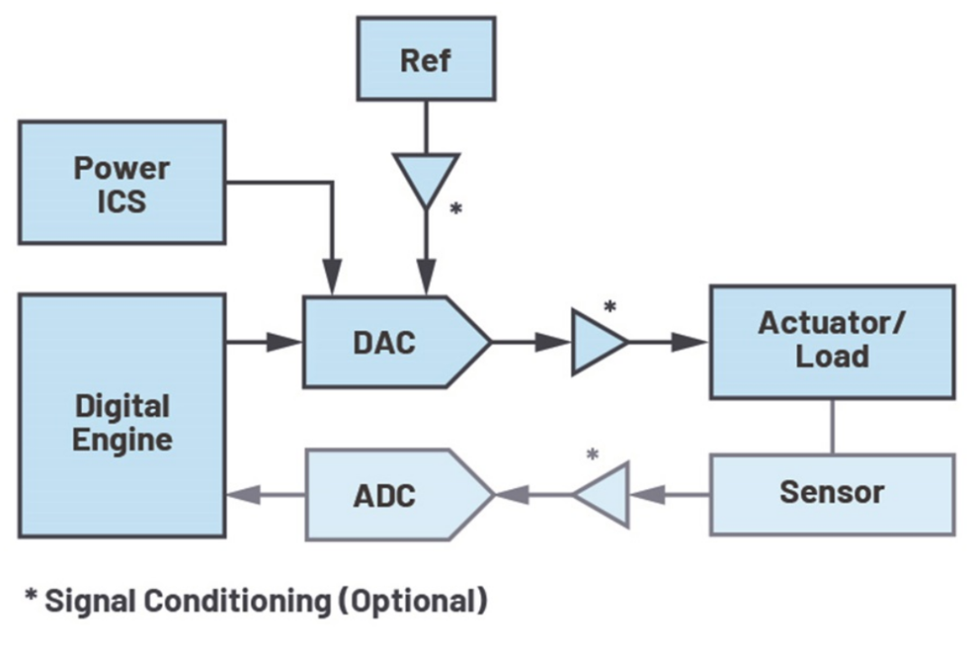
Figure 2. DAC Signal Chain Schematic.
Closed-loop solutions require additional components and manipulate digital data through software to provide more accurate outputs. If these additional resources cannot be added for various reasons (space, cost, etc.), open-loop solutions are still effective—as long as they can provide the required precision. This article explains how to perform open-loop calibration to help address this situation.
Theoretically, eliminating gain and offset errors (which are constant in the absence of external influences) through calibration is a straightforward procedure. The linear region of the DAC transfer function can be modeled as a line described by the following equation:

Where:
y is the output.
m is the slope of the transfer function accounting for gain error (as shown by the purple line in Figure 1).
x is the DAC input.
c is the offset voltage (as shown by the blue line in Figure 1).
Ideally, m is always 1, and c is always 0. In practice, the gain and offset errors of the DAC are considered, and once known, corrections can be made at the DAC input to achieve a digital output closer to the ideal DAC output. Multiplying the digital DAC input by the reciprocal of the gain error can eliminate the gain error. Adding the negative of the measured offset error to the digital DAC input can eliminate the offset error.
The following formula shows how to calculate the correct DAC input to produce the desired voltage:

Where:
Note that the offset error can be either positive or negative.
How to Successfully Calibrate a DAC Signal Chain
This section illustrates how to practically calibrate the offset and gain in a DAC signal chain using the AD5676R as an example. All measurements were made using the EVAL-AD5676 evaluation kit, enabling the internal reference voltage source of the AD5676R. The EVAL-AD5676 board and measurement setup are part of the signal chain we measured in the example. Each component in this signal chain (power ICs on the board, AD5676R, parasitic effects introduced by layout and connectors, etc.) contributes to the system error. Our intention is to demonstrate how to calibrate this system, providing a template for any other system.
Using the EVAL-SDP-CB1Z Blackfin® SDP control board (SDP-B) to communicate with the AD5676R on the EVAL-AD5676 evaluation kit, and using an 8-digit DMM to measure the output voltage VOUT0. A climate chamber is used to control the temperature of the entire system (composed of EVAL-SDP-CB1Z, EVAL-AD5676, and the built-in reference voltage source of the AD5676R).
The EVAL-AD5676 is powered on as described in the user guide, and the link configuration is shown in Table 3.
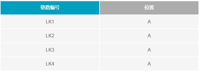
Table 3. Jumper Configuration for the EVAL-AD5676 Evaluation Board Used for the Measurements Described
First, evaluate the signal chain error without calibration (NoCal) at different temperatures. Considering the ideal and measured LSB differences for a specific input code, calculate the output error. This error includes both internal and external errors of the overall signal chain on the DAC and the EVAL-AD5676 board. The uncalibrated output error is shown in Figure 3.
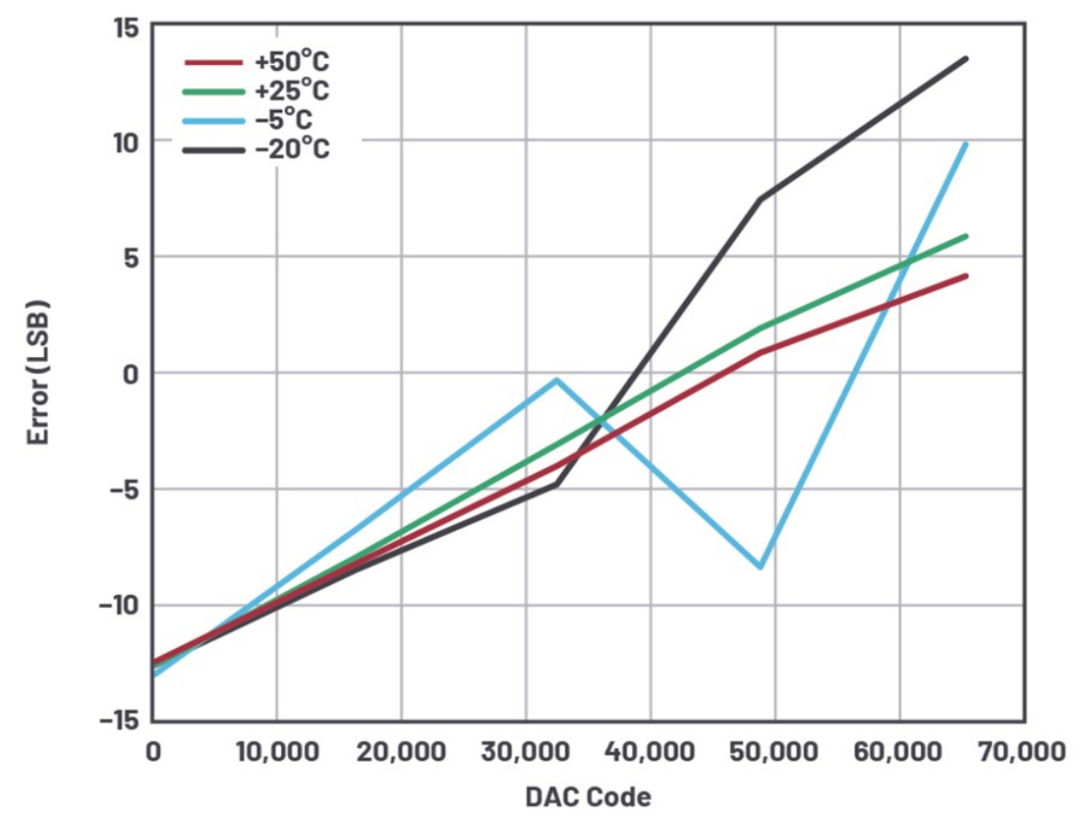
Figure 3. EVAL-AD5676 Output Error (LSB), No Calibration.
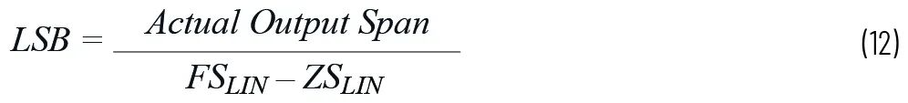
To calculate the offset and gain errors and the corresponding correction codes, information is needed from the transfer function. This requires two points: one data point close to zero (ZSLIN) and another close to full scale (FSLIN). The rationale is to work within the linear region of the DAC. This information is typically provided along with INL and DNL specifications, most likely in the footnotes of the specification sheet. For example, for the AD5676R, the linear region is from digital code 256 to digital code 65280.
Figure 4 explains the linear region of the DAC.
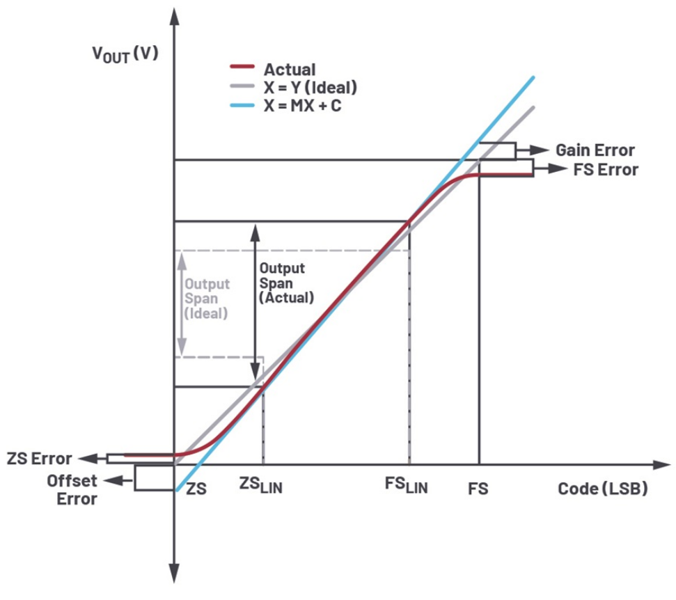
Figure 4. Transfer Function and Errors of a Unipolar Voltage DAC.
Once the ZSLIN and FSLIN codes are determined, we can collect the measurement results needed for calibration, namely the DAC voltage outputs at these two digital codes (VOUT at ZSLIN and VOUT at FSLIN), along with several other digital codes in between (¼ scale, mid-scale, and ¾ scale).
Measurements should be collected at the operating temperature of the application. If this is not possible, once the two main data points are collected at ambient temperature, the required information can be derived using the datasheets of the devices in the signal chain.
Each device in the signal chain contributes to the error, and each board is different, so calibration should be performed individually.
TempCal: Operating Temperature Calibration
Optimal calibration can be achieved by measuring the errors at the operating temperature of the application and performing system corrections when writing to the DAC to update the output.
To calibrate the DAC using this method, measure the DAC outputs corresponding to the digital codes ZSLIN and FSLIN at the expected operating temperature of the system. Construct the transfer function as follows:


Where:
VOE = Offset error (V)
VFS,LIN,ACT = Actual output at FSLIN
VZS,LIN,ACT = Actual output at ZSLIN
VFS,LIN,IDEAL = Ideal output at FSLIN
VZS,LIN,IDEAL = Ideal output at ZSLIN
Note that the offset error can be either positive or negative.
Figure 5 shows the output error achieved using the TempCal method with the EVAL-AD5676 evaluation kit.
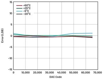
Figure 5. System Output Error (LSB) Using TempCal at Different Temperatures.
If it is not possible to measure the errors at the operating temperature of the application, high-level calibration can still be achieved using the AD5676R datasheet and the DAC transfer function calibrated at ambient temperature.
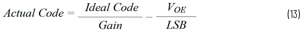
To calibrate the DAC using this method, measure the DAC outputs corresponding to the digital codes ZSLIN and FSLIN at ambient temperature. By calculating the gain and offset errors at ambient temperature and applying the formula 14, construct the transfer function as described in the TempCal section.
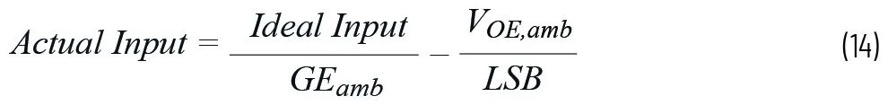
Where:
GEamb = Gain error at ambient temperature
VOE,amb = Offset error at ambient temperature (V)
Calibrating the DAC signal chain at ambient temperature can address system-level errors. However, the variations in external errors caused by temperature changes are not considered; therefore, this calibration method is not as precise as the TempCal method.
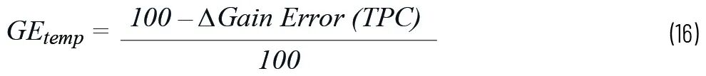
The drift of internal errors (i.e., offset and gain errors) of the DAC due to temperature changes can be addressed using the specifications in the datasheet. This is what we refer to as SpecCal. Typical values for offset error drift are listed in the technical specifications table of the AD5676R datasheet, and the typical performance parameters (TPC) representing the direction of error drift with respect to temperature are provided.

The variation of gain error due to temperature is represented by the TPC of gain error with respect to temperature. From the figure, determine the gain error in % FSR, then apply formula 16.
Once the offset and gain errors at the operating temperature are estimated, we can use formula 17 to determine the input code corresponding to the SpecCal output.
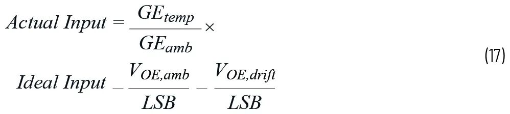
Where:

Figure 6 shows the output error achieved using the SpecCal method with the EVAL-AD5676 evaluation kit.
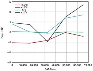
Figure 6. System Output Error (LSB) Using SpecCal at Different Temperatures.
This example used the internal reference voltage source. An external reference voltage source may increase overall error. The errors caused by the reference voltage source can be addressed using the reference voltage source datasheet and considering the reference voltage drift at the target temperature. Changes in the reference voltage will alter the actual output range, thereby changing the size of the LSB. Using an external reference voltage source should resolve this issue. The TPC of the relationship between temperature and output voltage can be used to determine the changes in output range caused by reference voltage drift.
Where:
 Conclusion
This article outlines some of the main causes of DAC signal chain errors, including the internal errors defined in the datasheet and the system-level errors that vary with the system and must be considered in open-loop applications.
This article discusses two calibration methods: one for cases where the DAC can be calibrated at the system’s operating temperature, and the other for cases where calibration cannot be performed at the operating temperature but can be measured at ambient temperature. The second method uses the TPC and technical specifications provided in the datasheets of the DAC and other ICs in the signal chain to address the drift of gain and offset errors.
The TempCal method can achieve much better accuracy than the SpecCal method. For example, for the EVAL-AD5676 board at 50°C, Figure 7 shows that the accuracy achieved by the TempCal method is very close to the ideal accuracy, while the SpecCal method shows some improvement relative to the NoCal data.
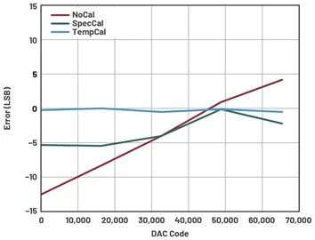
Figure 7. System Output Error (LSB) for NoCal, SpecCal, and 50°C TempCal.
Temperature variations have a significant impact on the accuracy of electronic systems. Calibrating at the system’s operating temperature can eliminate most errors. If this is not possible, the information provided in the datasheets of the DAC and other ICs can be used to address temperature variations and achieve acceptable accuracy.
👇 Click to Explore ADI’s “Chip” World
··