 The Xilinx DMA/Bridge Subsystem for PCI Express (PCIE) IP (XDMA) significantly reduces the difficulty for FPGA developers in using the PCIE interface. By implementing a simple BD design, FPGA-side logic design can be achieved, and with open drivers and example code, developers can quickly establish end-to-end communication over PCIE.Currently, Xilinx has released drivers for XDMA on Win/Linux systems. However, the official statement clearly indicates that the drivers only support the X86 platform and do not support ARM platforms. This can be confirmed through discussions between users and Xilinx officials on the AMD official Q&A platform.In this tutorial, I will share how to compile and debug XDMA on the RK3588 platform. Based on my experience, this tutorial is applicable to all ARM devices.This tutorial is mainly divided into the following four points:
- 1. Preliminary preparation, mainly explaining the required hardware devices and software tools;
- 2. FPGA-side XDMA configuration, mainly explaining how to quickly configure test routines in VIVADO;
- 3. Device connection;
- 4. ARM-side driver compilation, mainly explaining how to use the SDK to compile the driver files suitable for RK3588;
- 5. ARM-side read/write testing;
- 6. Summary and extension
1. Preliminary PreparationTo ensure the smoothness of the subsequent tutorial, I will list all the necessary tools and files in the preliminary preparation stage, as follows, starting with the hardware devices:
- A computer with Vivado and a virtual machine (ARM SDK) installed;
- A set of FPGA boards equipped with PCIe golden fingers;
- A set of RK3588 boards equipped with PCIe slots;
In addition to the above essential debugging hardware, the following resources should also be prepared in advance:
- RK3588 official SDK files;
- XDMA practical open-source tutorial;
- Download link: https://github.com/WangXuan95/Xilinx-FPGA-PCIe-XDMA-Tutorial
- XDMA Linux driver open-source files:
- Download link: https://github.com/Xilinx/dma_ip_drivers
During the debugging phase of RK3588, I generally prefer to use SSH for remote operations on the device. If you are interested in this part, feel free to leave a comment, and I will also summarize it into a tutorial document in subsequent chapters.2. FPGA Side ConfigurationStep 1. Create a new project on the FPGA side and create a Block Design, which will not be detailed here;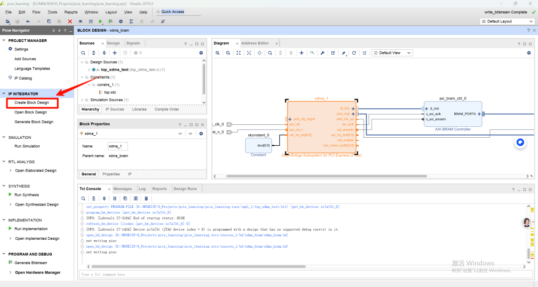 Step 2. Brief description of BD design;
- Click the + sign to search for XDMA and double-click to instantiate the IP;
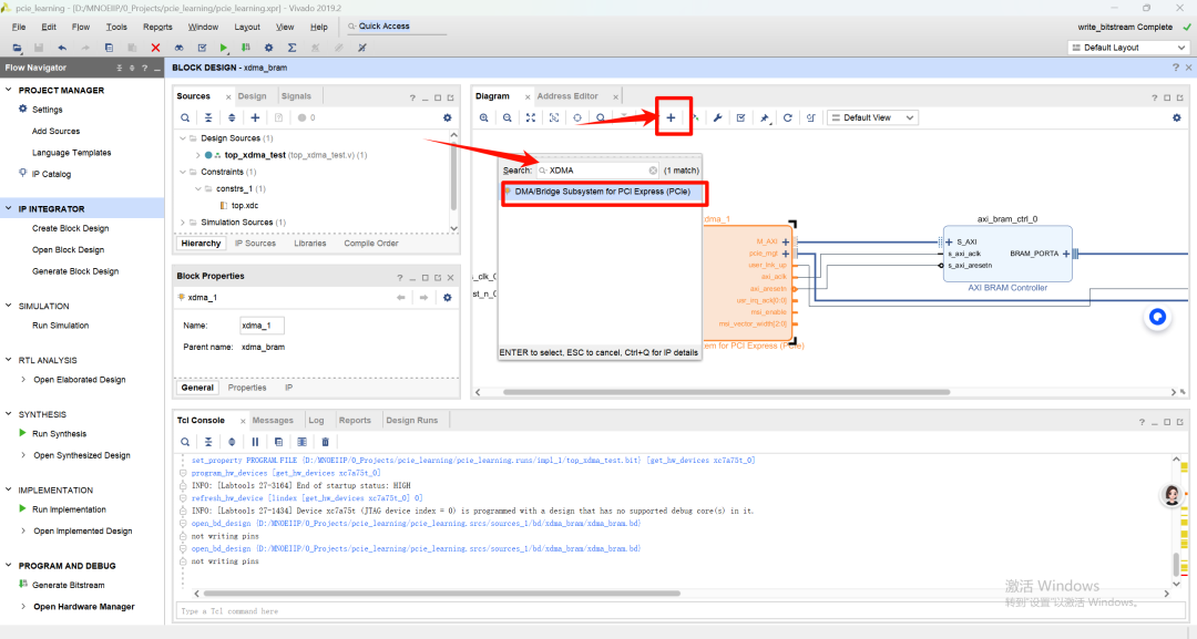 The following is the configuration of the IP; please select reasonable configurations based on the board, and keep other pages as default;
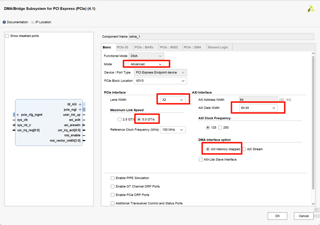
- Click the + sign to search for BRAM and select AXI BRAM Controller IP;
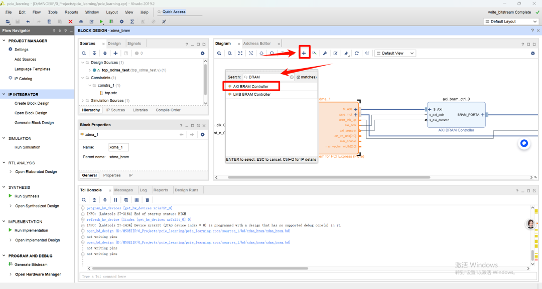 Configuration as follows:
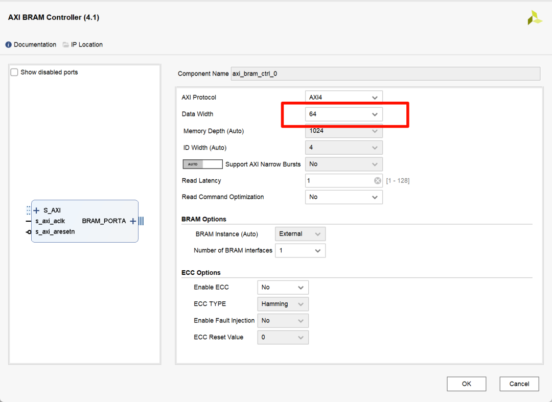
- Instantiate a constant IP of 1’b0;
- Then connect the above three IPs;
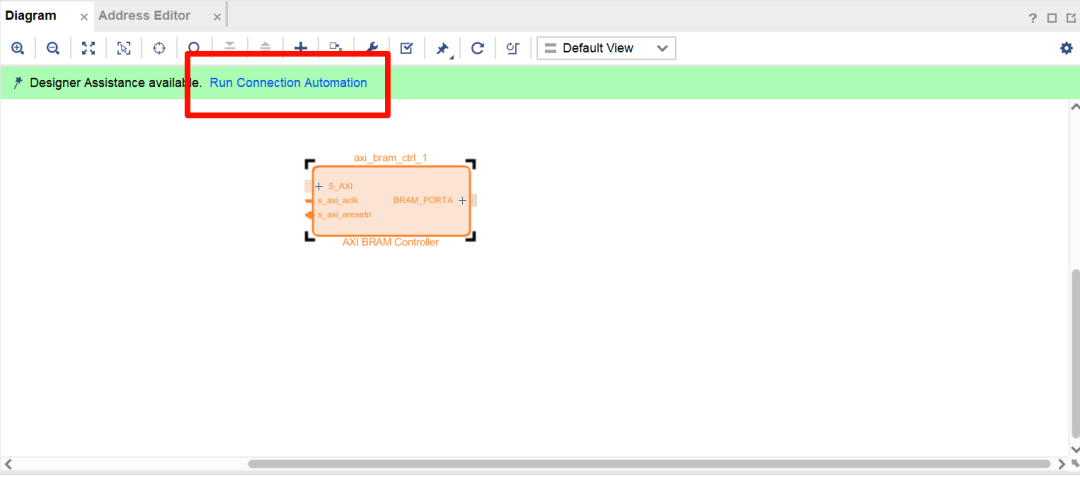
- Click Run Connection Automation at the top of the BD;
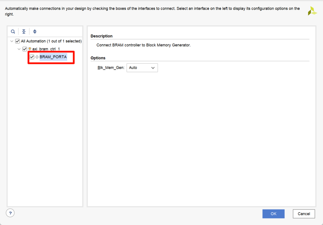
- Select the BRAM_PORTA under AXI BRAM Controller IP to execute the automatic connection;
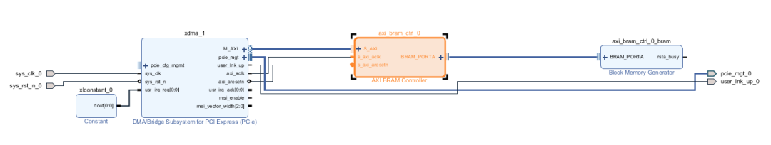
- Connect the above IPs and output the signals as shown;
 Step 3. Create the TOP layer and pin constraint file;
- Select the BD design and choose create wrapper;
- Create the TOP file;
`timescale 1ns / 1ps
module top_xdma_test(    output wire       o_led0,    input  wire       i_pcie_rstn,    input  wire       i_pcie_refclkp, i_pcie_refclkn,    input  wire [1:0] i_pcie_rxp, i_pcie_rxn,    output wire [1:0] o_pcie_txp, o_pcie_txn);
wire  pcie_rstn;wire  pcie_refclk;
// Ref clock input buffer ----------------------------------------------IBUFDS_GTE2 refclk_ibuf (    .CEB             ( 1'b0              ),    .I               ( i_pcie_refclkp    ),    .IB              ( i_pcie_refclkn    ),    .O               ( pcie_refclk       ),    .ODIV2           (                   ));
// Reset input buffer ----------------------------------------------IBUF   sys_reset_n_ibuf (    .I               ( i_pcie_rstn       ),    .O               ( pcie_rstn         ));
// block design's top (the HDL wrapper) ----------------------------------------------xdma_bram_wrapper xdma_bram_wrapper_i (    .pcie_mgt_0_rxn  ( i_pcie_rxn        ),    .pcie_mgt_0_rxp  ( i_pcie_rxp        ),    .pcie_mgt_0_txn  ( o_pcie_txn        ),    .pcie_mgt_0_txp  ( o_pcie_txp        ),    .sys_clk_0       ( pcie_refclk       ),    .sys_rst_n_0     ( pcie_rstn         ),    .user_lnk_up_0   ( o_led0            ));
endmodule- Create the pin constraint xdc file;
set_property -dict { PACKAGE_PIN M16 IOSTANDARD LVCMOS33 } [get_ports { o_led0 }];
set_property -dict { PACKAGE_PIN Y18 IOSTANDARD LVCMOS33} [get_ports i_pcie_rstn];   # PCIe reset
set_property PACKAGE_PIN F10  [get_ports { i_pcie_refclkp }];     # PCIe reference clock
set_property PACKAGE_PIN D7   [get_ports { o_pcie_txp[0] }];      # PCIe TX signal 0
set_property PACKAGE_PIN B6   [get_ports { o_pcie_txp[1] }];
set_property PACKAGE_PIN D9   [get_ports { i_pcie_rxp[0] }];      # PCIe RX signal 0
set_property PACKAGE_PIN B10  [get_ports { i_pcie_rxp[1] }];
Finally, generate the bit file or bin file, download or program it into the corresponding unit of the FPGA to complete the FPGA-side testing program.3. Device ConnectionThe order of PCIe connection and FPGA bitstream programming is particularly critical. I recommend following the order below to ensure the device operates normally while preventing damage to the device.Step 1. Insert the PCIe golden finger of the FPGA device into the PCIe slot of the ARM device.Step 2. Power on the ARM device; once the device starts, it will enter the system;Step 3. Download the program to the FPGA via JTAG;Step 4. Restart the ARM device, ensuring that the FPGA does not lose power. If the FPGA-side program is already solidified, steps 3-4 can be omitted;Step 5. After restarting, enter lspci in the terminal to check if the FPGA device is present. It may require multiple restarts; sometimes the FPGA configuration is slow, and you need to wait for the FPGA to be configured before the ARM device can detect the FPGA PCIe device.
lspci(To be continued)