Snapdragon 820 Specifications
The Snapdragon 820 features Qualcomm’s proprietary 64-bit architecture, utilizing four Kryo cores with a maximum clock speed of 2.2GHz, produced using Samsung’s 14nm FinFET process. It supports Quick Charge 3.0 technology and is equipped with the Adreno 530 graphics processing unit, while the DSP digital signal processor is the Hexagon 680. For image processing capabilities, it adopts the new Spectra 14-bit dual ISP processor, which can support up to 28 million pixels at 30fps with a throughput of 1.2GPix/sec (1.2 billion pixels per second).
The Snapdragon 820 supports dual-channel LPDDR4-1866 memory, eMMC 5.1, UFS2.0 (Gear3), SD 3.0 (UH S-I), and USB3.0 input/output, along with support for general-purpose loan compression technology.
Snapdragon 820 modem specifications: the 820 continues to lead the market, equipped with the new X12 LTE modem, utilizing the WTR3925 fourth-generation LTE multimode transceiver, supporting global frequency bands, full-band TDD-LTE and FDD-LTE, WCDMA (DB-DC-HSDPA/DC-HSUPA), TD-SCDMA, CDMA 1x/EVDO, and GSM/EDGE, supporting LTE Cat.12 with a maximum download speed of 600Mbps and LTE Cat.13 with a maximum upload speed of 150Mbps. Coupled with the WTR3950 transceiver, it can also support LTE-U on unlicensed spectrum.
Snapdragon 820 wireless network specifications: the Snapdragon 820 features Qualcomm VIVE 802.11ac, supporting tri-band Wi-Fi, and supports Qualcomm’s 2X2 MU-MIMO (multi-user multiple input multiple output) technology launched in the summer.
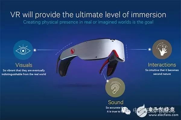
Snapdragon 820 VR Software Development Kit
Qualcomm’s Snapdragon VR SDK will be released in the second quarter, significantly simplifying the development of VR applications, including games, 360-degree videos, interactive education, and entertainment.
Qualcomm claims that this development package can greatly reduce rendering latency, supporting stereo rendering, lens correction, color correction, distortion correction, and achieving a maximum resolution of 3200×1800 at 60fps.
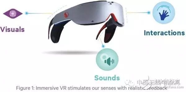
Qualcomm states that Snapdragon 820 VR applications are not only compatible with mobile devices like smartphones and tablets but can also be integrated into headsets without the need for an additional high-end PC platform.
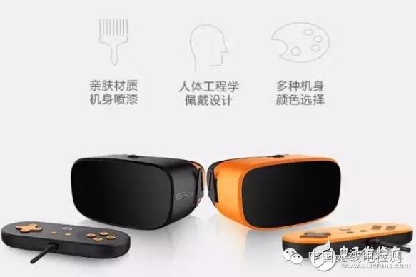
Snapdragon 820: Pico Neo Developer Edition
The Pico Neo Developer Edition can be used without a smartphone and adopts a split design, where the processor, memory, and battery are housed in a separate controller connected to the headset via a Type C data cable, priced at 3399 yuan. In addition to the Pico Neo, the launch event also introduced PUI, an external position tracking kit, Pico industry application solutions, and the latest version of Pico SDK.
Thunder Software Technology Snapdragon 820 VR All-in-One Reference Design
Thunder Software Technology released a reference design for the Snapdragon 820 VR all-in-one unit, covering various aspects from screen, optics, to PCBA, and thermal design, and is equipped with a self-developed VR OS, providing a full turnkey solution for lower-level driver and energy efficiency optimization, latency distortion motion tracking algorithms, Android M trimming, optimization, and upper-layer applications and launcher.
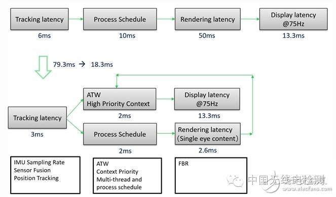
This reference design is based on the Qualcomm Snapdragon 820 platform, with options for single-eye 1440×1440/90Hz or 2560×1440/75Hz screens, paired with a 95° horizontal field of view lens, with latency below 19 milliseconds (head pose data transmission latency: 3ms, software algorithm processing and scheduling: 2ms, data rendering and screen display parallel processing: 13.3ms, totaling 18.3ms). Additionally, this design supports dual-band Wi-Fi, Bluetooth 4.1 high-speed transmission, and Qualcomm Quick Charge functionalities.
At the operating system level, Thunder Software Technology’s VR OS is deeply customized at the Kernel, Runtime, and Framework levels, reducing the native Android latency from nearly 80ms to below 19ms through proprietary deep optimization and core algorithms. Moreover, for VR display and latency, Thunder Software Technology has focused on developing relevant core algorithms, including ATW, Frontbuffer rendering, Context Priority, distortion/color dispersion correction, and Sensor fusion.
VR application developers can utilize this reference design platform to validate personalized applications, third-party interactions, and assess the best experience for relevant applications. VR manufacturers can swiftly productize using this platform, potentially bringing products to market within 2 months.
MediaTek Helio X30
MediaTek released the first generation of deca-core mobile processors Helio X20/X25, but this is just the beginning, as MediaTek has long been preparing the second generation deca-core, named Helio X30.
It is said that Helio X30 will be equipped with two 2.8GHz A57 cores, four 2.2GHz A53 cores, and four 2GHz A53 cores, utilizing a 10nm process.
The GPU will abandon ARM Mali in favor of MediaTek’s more customized Imagination PowerVR, specifically the PowerVR 7XT series, although it will still only have four cores.
Additionally, Helio X30 will support 26 million pixel cameras, dual main cameras, VR, and integrate an all-network baseband, supporting up to LTE Cat.13.
Helio X30 will be launched mid-year and enter mass production by the end of the year, supporting LPDDR4, UFS, and enabling 2Kx2K display VR support through mobile insertion, positioning it as a flagship mobile processor.
Samsung Exynos 8890
The Exynos 8890 octa-core processor is Samsung’s second SoC based on 14nm FinFET technology. Unlike the Exynos 7420, the Exynos 8890 is a true integrated solution, combining CPU/GPU/ISP and the latest LTE Cat.12/13 baseband. It features Samsung’s first 64-bit ARMv8 architecture CPU, known as the Mongoose architecture.
The CPU consists of 4 Mongoose cores and 4 A53 cores, enhancing multi-core scheduling capabilities and improving multitasking/process performance, thereby optimizing the utilization efficiency of the 8 cores.
While Samsung has not mentioned much about the GPU, the specifications for the Mali-T880 MP12 are exceptionally powerful, boasting 12 graphics cores, significantly outperforming the Kirin 950’s Mali-T880 MP4. Officially, this is prepared for immersive 3D gaming and virtual reality experiences.
The baseband also catches up with Qualcomm’s capabilities, achieving downlink Cat.12 with a maximum download speed of 600Mbps, and uplink Cat.13 with a maximum upload speed of 150Mbps, matching the domestic 4G download speeds and comparable to the Snapdragon 820.
STMicroelectronics STM32
The STM32F4 series MCU, based on the ARM Cortex-M4, utilizes STMicroelectronics’ NVM technology and ART accelerator, achieving a processing performance of 225 DMIPS/608 CoreMark at a working frequency of up to 180MHz when executing from flash memory, which is the highest benchmark score achieved by any microcontroller product based on the Cortex-M core to date.
Thanks to dynamic power adjustment features, the current consumption range during flash execution is from 89 µA/MHz for the STM32F410 to 260µA/MHz for the STM32F439.
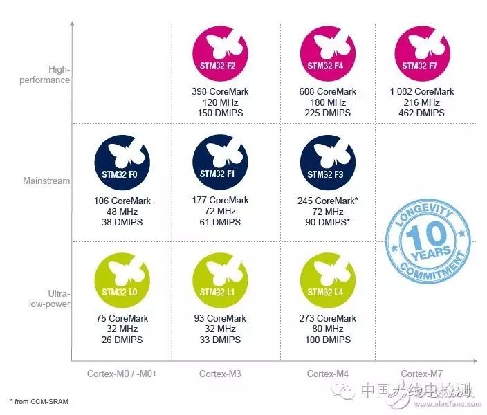
The STM32F4 series includes eight mutually compatible digital signal controller (DSC) product lines, perfectly combining the real-time control capabilities of MCUs with the signal processing capabilities of DSPs:
Advanced Series
• STM32F469/479 – 180 MHz CPU/225 DMIPS, up to 2 MB dual-bank flash, with SDRAM and QSPI interfaces, Chrom-ART Accelerator™, LCD-TFT controller, and MPI-DSI interface
• STM32F429/439 – 180 MHz CPU/225 DMIPS, up to 2MB dual-bank flash, with SDRAM interface, Chrom-ART Accelerator™ and LCD-TFT controller
• STM32F427/437 – 180 MHz CPU/225 DMIPS, up to 2 MB dual-bank flash, with SDRAM interface, Chrom-ART Accelerator™, serial audio interface, higher performance, and lower static power consumption
Basic Series
• STM32F446 – 180 MHz/225 DMIPS, up to 512 KB Flash, with Dual Quad SPI and SDRAM interfaces
• STM32F407/417 – 168 MHz CPU/210 DMIPS, up to 1MB Flash, with added Ethernet MAC and camera interface
• STM32F405/415 – 168 MHz CPU/210 DMIPS, up to 1MB Flash, with advanced connectivity and encryption features
Basic Type Series
• STM32F411 – 100 MHz CPU/125 DMIPS, with excellent power efficiency, larger SRAM, and new intelligent DMA, optimizing power consumption for data batch processing (using a dynamic efficiency series with batch acquisition mode)
• STM32F410 – 100 MHz CPU/125 DMIPS, setting a new milestone for excellent power efficiency performance (89 µA/MHz in sleep mode and 6 µA), utilizing new intelligent DMA, optimizing power consumption for data batch processing (using a dynamic efficiency series with batch acquisition mode), equipped with true random number generators, low-power timers, and DAC
• STM32F401 – 84 MHz CPU/105 DMIPS, the smallest and most cost-effective solution, with outstanding power efficiency (dynamic efficiency series)
Applications
Disassembly of the Samsung Gear VR revealed that the main control chip used is the STM32F401 A5009V0 TW 435 from STMicroelectronics, which is the STM32F4 series 32-bit ARM Cortex-M4 microcontroller unit.
Many other VR devices also utilize this series of microcontrollers.
Rockchip RK3399
Powerful big.LITTLE CPU architecture + powerful Mali-T860MP4 GPU
The RK3399’s CPU employs a big.LITTLE architecture, featuring dual Cortex-A72 big cores and four Cortex-A53 small cores, significantly optimizing integer, floating point, and memory performance, leading to revolutionary improvements in overall performance, power consumption, and core area.
The RK3399’s GPU utilizes the next-generation high-end image processor Mali-T860, integrating more bandwidth compression technologies such as intelligent layering, ASTC, and local pixel storage, and supports more graphics and computing interfaces, with overall performance improved by 45% compared to the previous generation.
RK3399 Performance Advantages
Not only is the CPU and GPU more advanced, but the Rockchip RK3399 processor also possesses the following unique advantages:
1. Integrated dual USB3.0 Type-C interfaces, supporting Type-C Display Port audio and video output.
2. Dual ISP pixel processing capability of up to 800MPix/s, supporting simultaneous input of dual camera data, enabling advanced processing such as 3D and depth information extraction.
3. MIPI/eDP interfaces, supporting 2560×1600 screen display and dual-screen display.
4. HDMI2.0 interface, H.265/H.264/VP9 4K@60fps video decoding and display.
5. Built-in PCI-e interface, supporting PCI-e based high-speed Wi-Fi and storage expansion.
6. Supports 8-channel digital microphone array input.
7. Comprehensive system support: compatible with Android, Linux, and other operating systems.
RK3399-Based VR Solutions
1. Exceptional 4K 360-degree panoramic video decoding capability, compatible with standard 2D and 3D sources
For immersive VR products, the 360-degree video experience is a hard requirement from the consumer market. With the strong push from 360-degree VR cinemas, 360-degree VR video applications, and 360-degree VR short films, hardware devices supporting 360-degree panoramic video will become standard in VR products. Rockchip’s mainstream processors can support 4K resolution 360-degree panoramic video decoding and are also compatible with standard 2D and 3D sources, providing powerful hardware capabilities at the application layer.
2. Deeply optimized low-latency technology for VR, with overall latency below 20ms, improving more than five times compared to unoptimized Android systems
The VR experience involves a complex technical processing workflow. From sensor acquisition, transmission, game engine processing, driving hardware rendering images, to liquid crystal pixel color switching, every step generates latency. Currently, the globally recognized acceptable latency for VR is below 20ms; otherwise, it can cause dizziness and nausea. Most VR devices currently do not meet this standard.
To achieve the ideal value, comprehensive hardware and software optimization is necessary. Rockchip employs low-latency rendering technology, calculating a new frame based on the latest sensor orientation information while keeping the position unchanged, then submitting it to the display. Coupled with optimizations at the driver and image engine levels, a comfortable visual environment can be presented, improving more than five times compared to unoptimized Android systems.
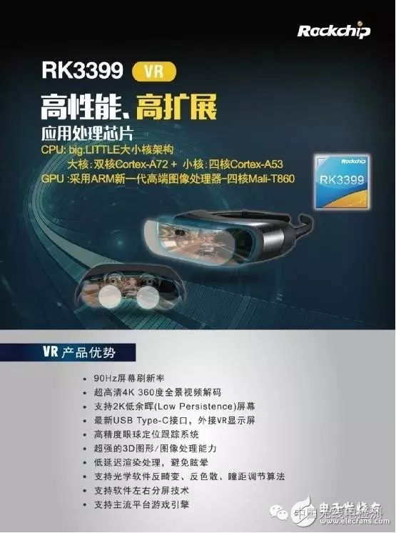
3. Display refresh rate exceeding 75Hz
The screen refresh rate is a crucial parameter that significantly impacts the VR product experience. Rockchip supports screen refresh rates exceeding 75Hz, far surpassing the standard 60Hz refresh rate of ordinary consumer-grade VR products. A sufficiently high frame rate solution will quickly eliminate industry barriers, allowing more brands and manufacturers to enter the market rapidly.
4. Support for 2K/dual FHD high-resolution screens
For VR display hardware support, Rockchip has supported 2K/dual FHD high-resolution screens. This hardware specification is also a mainstream configuration in high-end VR products, facilitating the rapid mass production of terminal products using its solutions.
5. Support for optical software anti-distortion, anti-dispersion, and interpupillary distance adjustment algorithms
Rockchip’s VR software technology optimizations are highly targeted. For issues such as distortion, color difference, and edge blurring caused by VR products, automatic corrections can be achieved through software detection and adjustments, implementing anti-distortion, anti-dispersion, and interpupillary distance adjustment algorithms. This presents significant advantages for terminal mass production, compensating for traditional hardware manufacturers’ shortcomings in software technology and reducing brand manufacturers’ investments and time in hardware and software research and development costs.
6. Support for both software and hardware left-right split-screen methods
Rockchip’s left-right split-screen technology is quite mature, supporting both software and hardware left-right split-screen methods. It not only automatically adapts to resolutions excellently but also actively optimizes to ensure stability. Furthermore, based on low-level image technology, texture, lighting, image detail, and distortion control can achieve optimal visual experience effects. The immersive feeling is strong during gaming and 3D movie experiences.
7. Support for mainstream platform game engines
As a core partner of the ARM ecosystem, Rockchip’s flagship chip solutions feature high-performance CPUs and GPUs. For example, the well-known Mali-T760 and the latest Mali-T860. Based on higher-end image processors, Rockchip supports mainstream game engine technologies in VR products, including global real-time lighting engines such as Geomerics Enlighten in Unity, providing more stunning visual effects for images, lighting, scenes, textures, and details in VR games and visuals.
Allwinner H8/A8 Chips
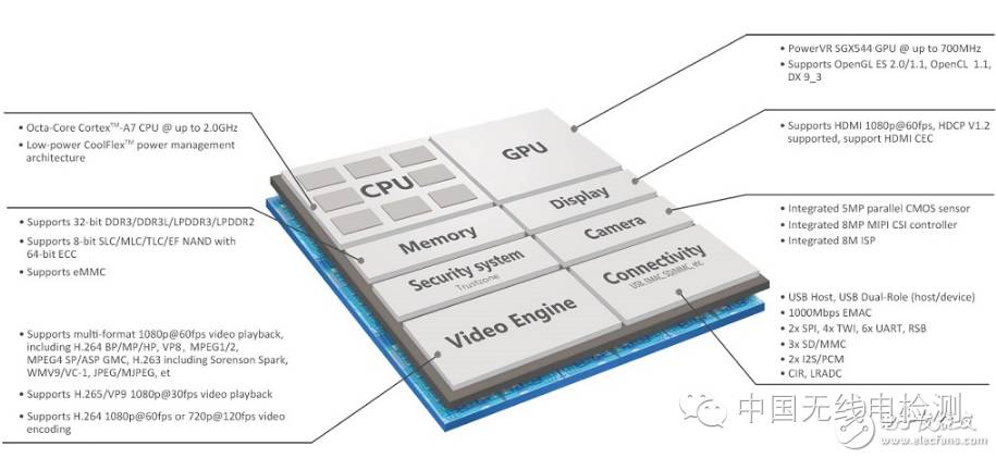
Allwinner H8, an octa-core based on TSMC’s latest leading 28nm manufacturing process, utilizes 8 ARM Cortex-A7 cores, supporting simultaneous high-speed operation of all 8 cores at 2.0GHz, paired with Imagination’s powerful PowerVR SGX544 image processing architecture, with a working frequency of around 700M.
In terms of multimedia, the H8 supports multi-format 1080p@60fps video codec, supports H.265/HEVC video processing, and integrates an 8M ISP image signal processing architecture, capable of supporting 8 million pixel cameras. For display, the H8 supports HDMI 1080p@60fps display, HDCP V1.2 protocol, and HDMI CEC. Additionally, the H8 integrates Allwinner’s next-generation color display technology, further enhancing image display quality. In fact, the H8 chip was initially applied in TV boxes.
Allwinner VR All-in-One Solution – H8vr
Allwinner Technology’s H8vr video all-in-one solution’s advantage is its ability to achieve mass production and optimize latency, power consumption, and multimedia aspects.
Reportedly, this solution features an open hardware system platform, open H8vr system SDK, with a finished product price around a thousand yuan, enabling mass production. Specifically, this solution is built on Allwinner’s dedicated VR chip, optimizing underlying algorithms and integrating ATW (Asynchronous Time Warp), FBR (Front Buffer Rendering), and employing the deeply optimized Nibiru VR all-in-one system for Android.
A significant highlight of the Allwinner H8vr video all-in-one solution is its characteristics of “low heat, low power consumption, and high integration”, with a smaller battery and lighter weight, alleviating the weight of the headset while also addressing the heat dissipation issues of the headset itself. Additionally, this solution supports up to 4K@60fps panoramic video, with deep collaboration optimizations across sensors, GPUs, displays, and optical lenses, supporting rich interaction methods, ensuring VR all-in-one performance and smooth UI experience.
Infotm Custom VR Chip
On November 9, 2015, the release of Tencent’s miniStation micro-game console attracted widespread attention.
The significant/unique features of Tencent’s miniStation include:
1. Wireless control of games displayed on the TV using a mobile phone;
2. Extremely low latency for both video and games;
3. Support for two-player same-screen gaming, one using a controller and the other using a mobile phone;
4. Seamless payment via mobile phone;
5. In-game communication with players through typing on the mobile phone;
6. Claimed collaboration with FIFA, allowing players to play manager mode on mobile and competitive mode on the console at home;
7. Support for VR headset devices, possibly connecting via a single cable or other methods.
Upon disassembly, the chip prominently displays two logos: Tencent and INFOTM. INFOTM is the English name of “Shanghai Infotm Microelectronics”, a company specializing in integrated circuit design, focusing on the research and development of mobile internet terminal application processor chips.
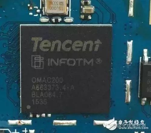
It appears that this custom chip was designed and manufactured by Infotm for Tencent, with both parties jointly branding the chip.
Reportedly, this custom chip’s basic information and functions include:
1. Internally adopting a high-performance 128-bit processor, said to differ from the mainstream 64-bit processors, achieving higher execution efficiency in data processing; thus enabling ultra-low latency data processing.
2. Capable of parallel processing multiple channels of multimedia data, including audio, video, and interactive data;
3. Employing advanced image processing and transmission technologies; these are crucial for achieving ultra-high wireless cross-screen transmission.
4. Specialized algorithm optimizations for VR technology, integrating more new technologies into future imaginative spaces.
However, further details about this chip are not available, reportedly due to a confidentiality agreement signed with Tencent.